Abstract
In this study, we designed a 5-bit K-band CMOS switch type phase shifter. In order to minimize phase and gain errors, a design technique for bits constituting the phase shifter was proposed. The proposed design technique has been achieved by adjusting the resonant frequencies of inductance and capacitance in the L-C-L T-type low pass filter structure. Through this, a method of optimizing the phase shifter with the T-type low pass filter structure was presented. The K-band 5-bit phase shifter was designed with a 65 nm CMOS process to verify the feasibility of the proposed design technique. The core size was 0.78 × 0.21 mm2. At the frequency ranges of 22.0 to 23.0 GHz, the insertion loss and RMS phase and gain errors were measured to be 7.44 ± 2.0 dB, 2.6°, and 1.2 dB, respectively.
1. Introduction
Recently, research and development of various RF circuits for array antenna systems has become active as the utilization of beamforming systems including 5G mobile communication has increased [1,2,3]. In particular, in the beamforming system, sophisticated phase variation is recognized as an essential technology. Therefore, various structures of phase shifters have already been introduced [4,5,6], and research to improve the performance of phase shifters is still actively underway.
In particular, passive-type phase shifters are widely used in beamforming systems because they allow bidirectional signal flow and have a relatively simple structure [7,8]. For such passive-type phase shifters, resolution, insertion loss, and phase and gain errors are major performance indicators. Because a phase shifter consists of several bits and operates in pass and shift modes for each bit, the phase shifter is characterized by having various operating states compared to other RF circuits [4,9,10]. As such, since the phase shifter operates in various states, it is important to minimize the phase and gain errors for each state of the phase shifter when considering the performance of the entire beamforming system. Therefore, various optimization techniques have been introduced to minimize the phase and gain errors for each state [7,10,11]. Most of these optimization techniques are based on mathematical analysis.
In this study, for the beamforming system in the flexible access common spectrum (FACS) millimeter-wave band [12], a 5-bit K-band complementary metal-oxide-semiconductor (CMOS) phase shifter was designed using the L-C-L T-type low pass structure. In order to minimize the root mean square (RMS) phase and gain errors of the phase shifter, a design technique was proposed that utilizes the resonances of the inductance and capacitance constituting each bit. In particular, the proposed design technique provides a method for graphically understanding the process of minimizing phase and gain error using phase and gain graphs according to the frequency of shift and pass modes. Based on this, the proposed design technique provides a method of obtaining the initial values of the inductors and capacitors constituting the phase shifter through impedance analysis using the equivalent circuits of the phase shifter. In addition, for further improvement of phase and gain errors, the 180° bit is assumed to be mounted on a differential amplifier located on a signal path passing through the phase shifter, and accordingly, the 180° bit was not included in the phase shifter of this study.
2. Proposed Design Technique of the T-Type Phase Shifter
In this study, the designed phase shifter consists of a total of five bits, excluding the 180° bit. When the 180° bit is implemented in a phase shifter, a large chip area is generally required compared to other bits. In addition, the 180° bit has a large insertion loss compared to other bits, and generally has a narrow bandwidth. On the other hand, it is relatively easy to configure the 180° bit in a typical differential amplifier structure rather than a phase shifter [12,13,14]. In this case, problems related to area, insertion loss, and bandwidth resulting from the 180° bit can be solved. As a representative example, the 180° phase shift function can be mounted on power amplifiers and low-noise amplifiers of differential structures [12,13,14]. Therefore, the 180° bit was not included in the phase shifter of this study.
Figure 1 shows the schematic of the unit-bit used in this study. All of five bits, from 5.625° bit to 90° bit, are designed to have the same structure of L-C-L T-type low pass filter structure. In Figure 1, RM1 is the parasitic resistance of the ON state M1. RM2 and CM2 are parasitic components in ON and OFF states of M2, respectively. In the pass and shift modes of each bit, M1 operates in ON and OFF states, respectively, and M2 operates in the opposite state to M1.
Figure 1.
T-type structure: (a) schematic of the used T-type structure, and equivalent circuits for the (b) shift and (c) pass modes.
In this study, for convenience of analysis, it is assumed that the terminal impedance is 50 Ω, and the resistance of the transistor is negligibly small when the transistor is in the ON state. In addition, when the transistor was in the OFF state, it was modeled as a drain-source parasitic capacitance. Such assumptions and simplifications are intended to obtain initial values of inductors and capacitors constituting the phase shifter. Therefore, in the final design stage should be accompanied by an optimization process through electromagnetic (EM) simulation, etc.
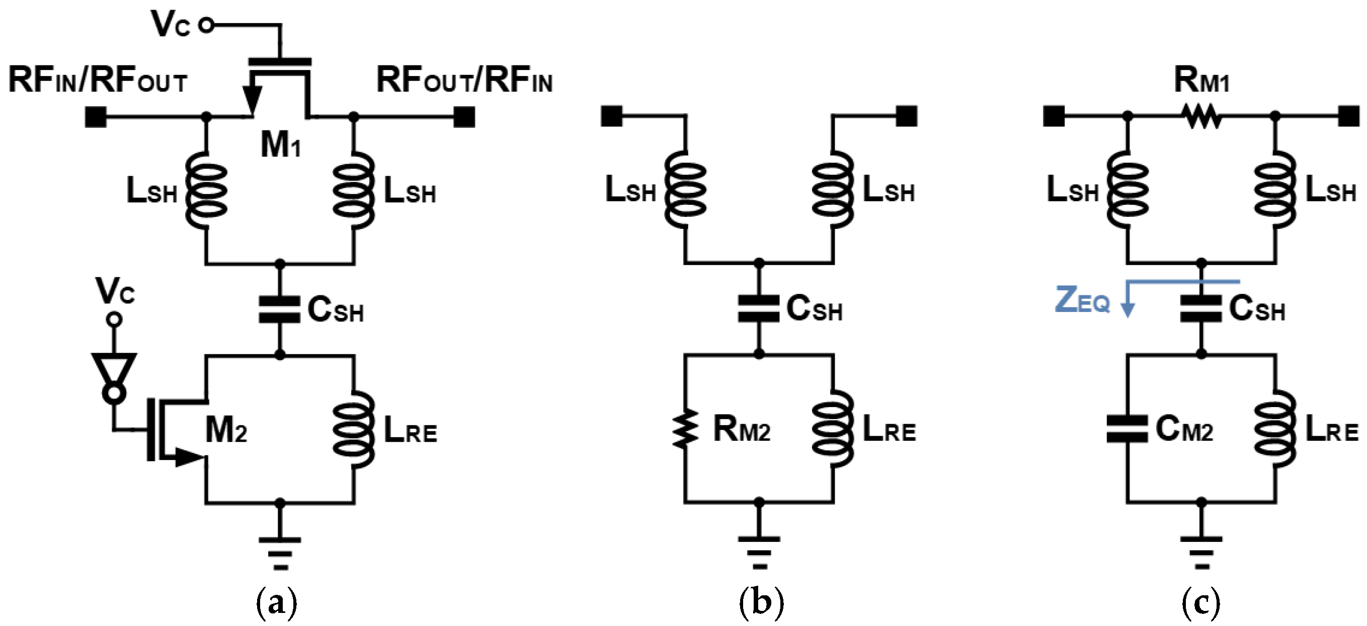
2.1. Analysis of the Operation of the Phase Shifter
In the shift mode, for the convenience of intuitive analysis, it is assumed that the impedance of RM2 is negligible compared to the impedances of LRE and CSH. Therefore, the equivalent circuit of the shift mode shown in Figure 1b may be considered as the T-network of LSH-CSH-LSH. At this time, for convenience of analysis, the parasitic capacitance of M1 in the OFF state in shift mode was ignored because it plays an incidental role in the analysis of this study. If the parasitic capacitance of M1 is considered, there is an effect of decreasing the required LSH value compared to the case not considered [15]. In this study, optimization was carried out in consideration of the parasitic capacitance of M1 in the final design stage of the phase shifter.
In the case of the pass mode, the equivalent circuits according to frequency are shown in detail in Figure 2. The ZEQ of Figure 1c in the pass mode is calculated as follows:
Figure 2.
Equivalent circuits for pass mode according to frequency: (a) ω < ωZEQ = 0, (b) ω = ωZEQ = 0, (c) ωZEQ = 0 < ω < ωZEQ = ∞, (d) ω = ωZEQ = ∞, and (e) ωZEQ = ∞ < ω.
In addition, the values of ω satisfying ZEQ = 0 and ZEQ = ∞ are calculated as follows:
The ZEQ values calculated in Equation (2) are utilized in the minimization technique of phase and gain errors described in Section 2.2 and Section 2.3.
2.2. Design Technique for Securing the Required Phase
A phase of each bit of a phase shifter is defined as a phase difference between shift and pass modes. Therefore, in order to improve the phase accuracy of each bit, the phases of shift and pass modes were first calculated. In this study, the phases in shift and pass modes were calculated as follows:
where ϕS21,Shift and ϕS21,Pass are phases of the shift and pass modes, respectively. In general, the phase in pass mode has a very small value. For each bit, the difference in phases calculated from Equations (3) and (4) becomes the phase of the corresponding bit. In this case, it is assumed that the termination impedance Z0 is 50 Ω. For convenience, ωP was defined as follows:
Here, ωP represents the frequency at which the phase of the output signal compared to the input signal changes to 90°, assuming that RM2 is sufficiently small in the shift mode of Figure 1b and the impedance by LRE is ignored. In this study, in order to make the phase of the pass mode close to zero, ZEQ is designed to be ∞ at the operating frequency. At this time, when the value of ωP is adjusted through LSH and CSH, the slope of Equation (3) is also adjusted. Accordingly, as shown in Figure 3a, a desired phase in the shift mode can be secured at a given operating frequency. In Figure 3a, ωP90 and ωP45 are shown as examples. Here, ωP90 and ωP45 are ωP values for phase shift of 90° and 45° at a given operating frequency, respectively. As a result, through this process, values of ωZEQ=∞ and ωP are set.
Figure 3.
Conceptual diagrams for securing required (a) phase and (b) gain.
2.3. Design Technique for Minimizing Gain Error
As a next step, a design was performed to minimize the gain error between shift and pass modes based on the previously determined values of ωZEQ = ∞ and ωP. Figure 3b shows a conceptual diagram for minimizing the gain error. As can be seen in Figure 3b, the gain in shift mode decreases as the frequency increases. On the other hand, in the case of pass mode, as can be predicted from Figure 2, the gain increases as the frequency increases in the region after the frequency satisfying ωZEQ = 0. Therefore, when the frequency satisfying ωZEQ = 0 is adjusted, the gain of shift and pass modes may be set equally at the operating frequency. In Figure 3b, ωM is defined as a frequency satisfying ωZEQ = 0.
Here, in order to maintain the minimized phase error previously described, the values of ωZEQ = ∞ and ωP determined in Section 2.2 must be maintained. Therefore, in order to maintain the values of ωZEQ = ∞ and ωP, the gain error can be minimized by adjusting the LRE, CM2, and CSH while maintaining the ratio of LSH to CSH and the ratio of LRE to CM2.
In conclusion, the design process of the proposed phase shifter can be summarized step by step as follows.
- Step 1: In the pass mode, the LRECM2 value is set so that ωZEQ = ∞, the frequency at which ZEQ becomes infinite, becomes the desired operating frequency. This process allows the phase in the pass mode to become zero.
- Step 2: In the shift mode, the frequency of the ωP determined by LSHCSH is adjusted to secure the desired phase difference at the desired operating frequency.
- Step 3: In the pass mode, ωM, the frequency at which ZEQ becomes zero, is adjusted so that gains in shift and pass modes are the same at the desired operating frequency. In this case, the value of LRE(CSH + CM2) is used to adjust the ωM.
- Step 4: Finally, the initial values of the inductors and capacitors constituting the unit-bit are set with LRE, LSH, CSH, and CM2 values satisfying the previous steps 1, 2, and 3.
3. Design Results of the Designed Phase Shifter
To verify the feasibility of the proposed design technique, a K-band phase shifter with L-C-L T-type low-pass filter structure using 65 nm RFCMOS process which provides eight metal layers.
Figure 4 shows the simulated phases for the shift and pass modes in the 45° and 90° bits. In this study, the values of ωP for 45° and 90° bits were designed to be 41.5 GHz and 23.4 GHz, respectively. Here, ωP45 and ωP90 present the values of ωP for 45° and 90° bits, respectively. As shown in Figure 4, simulation results of high-accuracy phase shift were obtained for both 45° and 90° bits.
Figure 4.
Simulated phases for shift and pass modes for (a) 45° and (b) 90° bits.
In addition, as shown in Figure 5, the values of ωM for 45° and 90° bits were designed to be 15.2 GHz and 16.5 GHz, respectively. Here, ωM45 and ωM90 present the values of ωM for 45° and 90° bits, respectively. As can be seen in Figure 5, the proposed design technique minimizes the gain error at a given operating frequency.
Figure 5.
Simulated gains for shift and pass modes for (a) 45° and (b) 90° bits.
In Table 1, the design parameters of the designed phase shifter were shown. The values of all active and passive devices were finally optimized using EM simulation after all bits were connected.
Table 1.
Size of the used transistors, inductors, and capacitors.
Figure 6 shows the configuration of the designed phase shifter, and each bit is designed with the schematic of the unit-bit of Figure 1. C90 with 56.3 fF is additionally used for matching between bits. Although 180° bit is not mounted on the designed phase shifter of this study, the 180° bit can be easily implemented by connecting two 90° bits designed in this study if a 180° bit is required.
Figure 6.
Overall structure of the designed phase shifter.
Figure 7 shows the simulated phase and gain characteristics. The effect of all passive devices, including interconnection lines and pads were considered through EM simulations. Decoupling capacitors are positioned between the pads for applying the control voltage VC for each bit to stabilize the VC. In this study, 1.0 V was used as VC for simulation and measurement.
Figure 7.
Simulated results: (a) phase and RMS phase error and (b) insertion loss and RMS gain error.
Figure 8 shows a photograph of the designed phase shifter with chip and core sizes of 960 × 400 μm2 and 780 × 210 μm2, respectively. Considering that the 180° bit is mounted on the amplifier of the differential structure, the 180° bit is not mounted on the phase shifter of this study, so it is designed in a compact size. We used bonding wire for VC pads for dc voltages, and RF input and output signals were measured through on-wafer probing to minimize measurement error.
Figure 8.
Chip photograph of the designed K-band CMOS phase shifter.
Figure 9 shows the measured phase and gain characteristics. In the frequency range of 22.0 GHz to 23.0 GHz, insertion loss, RMS phase error, and RMS gain error were measured as 7.44 ± 2.0 dB, <2.6°, and <1.2 dB, respectively. Compared to the simulation results, in the measurement results, insertion loss increased and RMS phase and gain errors were somewhat degraded. The main reason expected is that the accuracy of EM simulation in the design process of the 90° bit seems to have deteriorated. If the EM simulation accuracy for the 90° bit is improved, it is expected that RMS phase and gain errors can be improved. Accordingly, it is also expected that the measurement results of the phase shifter with a wider operating frequency range can be obtained.
Figure 9.
Measurement results: (a) phase and RMS phase error and (b) insertion loss and RMS gain error.
Table 2 shows the performance of the CMOS phase shifters available in the literature. As shown in Table 2, although the measurement results of the designed phase shifter deteriorated compared to the simulation results, the measurement results of the improved RMS phase error were obtained. In addition, the designed phase shifter has no 180° bit, resulting in the measurement results of competitive insertion loss. Thanks to the absence of the 180° bit, the proposed phase shifter has a compact core size when compared to previous 5-bit phase shifters.
Table 2.
Performance comparison of CMOS phase shifter.
4. Conclusions
In this study, a K-band CMOS phase shifter with L-C-L T-type low pass structure was designed. To reduce the RMS phase and gain errors, a design technique using resonances in the L-C-L T-type low pass structure was proposed. First, the phase was determined through optimization of two resonance frequencies for each bit. Based on the two determined resonance frequencies, the design parameters of each bit were set so that the gains of shift and pass modes became the same. To verify the feasibility of the proposed design technique, we designed the K-band 5-bit phase shifter using a 65 nm RFCMOS process. At the frequency ranges of 22.0 GHz and 23.0 GHz, the measured insertion loss, RMS phase error, and RMS gain error were 7.44 ± 2.0 dB, 2.6°, and 1.2 dB, respectively.
Author Contributions
Conceptualization, S.J. and C.P.; methodology, S.J., C.-Y.K. and C.P.; investigation, S.J.; supervision, C.P.; writing—original draft, S.J.; review and editing C.P. All authors have read and agreed to the published version of the manuscript.
Funding
This work was supported in part by the National Research Foundation of Korea (NRF) through the Korea Government (MSIT) under Grant NRF-2021R1A2C1013666 and in part by the National Research Foundation of Korea (NRF) through the Korea Government (MSIT) under Grant NRF-2021R1A4A1032580.
Data Availability Statement
All the material conducted in the study is mentioned in article.
Conflicts of Interest
The authors declare no conflict of interest.
References
- Lee, S.; Park, J.; Hong, S. Millimeter-Wave Multi-Band Reconfigurable Differential Power Divider for 5G Communication. IEEE Trans. Microw. Theory Tech. 2022, 70, 886–894. [Google Scholar] [CrossRef]
- Alhamed, A.; Kazan, O.; Gültepe, G.; Rebeiz, G.M. A Multiband/Multistandard 15–57 GHz Receive Phased-Array Module Based on 4 × 1 Beamformer IC and Supporting 5G NR FR2 Operation. IEEE Trans. Microw. Theory Tech. 2022, 70, 1732–1744. [Google Scholar] [CrossRef]
- Khan, B.; Tervo, N.; Jokinen, M.; Pärssinen, A.; Juntti, M. Statistical Digital Predistortion of 5G Millimeter-Wave RF Beamforming Transmitter Under Random Amplitude Variations. IEEE Trans. Microw. Theory Tech. 2022, 70, 4284–4296. [Google Scholar] [CrossRef]
- Lin, Y.-H.; Tsai, Z.-M. A Wideband Compact 5-Bit Phase Shifter with Low Loss and RMS Errors for 5G Applications. IEEE Microw. Wirel. Compon. Lett. 2021, 31, 1134–1137. [Google Scholar] [CrossRef]
- Wang, S.; Park, J.; Hong, S. A K-Band Variable-Gain Phase Shifter Based on Gilbert-Cell Vector Synthesizer with RC–RL Poly-Phase Filter. IEEE Microw. Wirel. Compon. Lett. 2021, 31, 393–396. [Google Scholar] [CrossRef]
- Liang, C.-J.; Zhang, Y.; Chiang, C.-W.; Huang, R.; Zhou, J.; Du, J.; Wen, K.-A.; Chang, M.-C.F.; Kuan, Y.-C. A K/Ka/V Triband Single-Signal-Path Receiver with Variable-Gain Low-Noise Amplifier and Constant-Gain Phase Shifter in 28-nm CMOS. IEEE Trans. Microw. Theory Tech. 2021, 69, 2579–2593. [Google Scholar] [CrossRef]
- Meghdadi, M.; Azizi, M.; Kiani, M.; Medi, A.; Atarodi, M. A 6-Bit CMOS Phase Shifter for S-Band. IEEE Trans. Microw. Theory Tech. 2020, 58, 3519–3526. [Google Scholar] [CrossRef]
- Sim, S.; Jeon, L.; Kim, J.-G. A Compact X-Band Bi-Directional Phased-Array T/R Chipset in 0.13 μm CMOS Technology. IEEE Trans. Microw. Theory Tech. 2013, 61, 562–569. [Google Scholar] [CrossRef]
- Kim, E.; Jeon, S. A Compact 275–320-GHz Reflection-Type Phase Shifter. IEEE Microw. Wirel. Compon. Lett. 2022, 32, 991–994. [Google Scholar] [CrossRef]
- Li, X.; Fu, H.; Ma, K.; Hu, J. A 2.4–4-GHz Wideband 7-Bit Phase Shifter with Low RMS Phase/Amplitude Error in 0.5-μm GaAs Technology. IEEE Trans. Microw. Theory Tech. 2022, 70, 1292–1301. [Google Scholar] [CrossRef]
- Kang, D.-W.; Lee, H.D.; Kim, C.-H.; Hong, S. Ku-band MMIC Phase Shifter Using a Parallel Resonator with 0.18-μm CMOS Technology. IEEE Trans. Microw. Theory Tech. 2006, 54, 294–301. [Google Scholar] [CrossRef]
- Jeong, H.; Lee, H.D.; Park, B.; Jang, S.; Kong, S.; Park, C. Three-Stacked CMOS Power Amplifier to Increase Output Power with Stability Enhancement for mm-Wave Beamforming Systems. IEEE Trans. Microw. Theory Tech. 2023, 71, 2450–2464. [Google Scholar] [CrossRef]
- Jang, S.; Lee, J.; Lee, J.-W.; Park, C. Design of K-Band Power Amplifier with 180-Degree Phase- Shift Function Using Low-Power CMOS Process. Appl. Sci. 2023, 13, 2501. [Google Scholar] [CrossRef]
- Jang, S.; Lee, J.; Park, C. K-Band CMOS Low-Noise Amplifier with 180° Phase Shift Function Using Cascode Structure. Electron. Lett. 2023, 59, e12908. [Google Scholar] [CrossRef]
- Kim, S.; Jang, S.; Lee, J.; Jeong, H.; Kim, K.-J.; Park, C. Ka-Band GaN HEMT Phase Shifter with T-Type Structure for Beamforming Applications. IEEE Microw. Wirel. Technol. Lett. 2023, 33, 743–746. [Google Scholar] [CrossRef]
- Shin, G.-S.; Kim, J.-S.; Oh, H.-M.; Choi, S.; Byeon, C.W.; Son, J.H.; Lee, J.H.; Kim, C.-Y. Low Insertion Loss, Compact 4-bit Phase Shifter in 65 nm CMOS for 5G Applications. IEEE Microw. Wirel. Compon. Lett. 2016, 26, 37–39. [Google Scholar] [CrossRef]
- Jung, M.; Min, B.-W. A Compact Ka-Band 4-bit Phase Shifter with Low Group Delay Deviation. IEEE Microw. Wirel. Compon. Lett. 2020, 30, 414–416. [Google Scholar] [CrossRef]
- Tsai, J.-H.; Tung, Y.-L.; Lin, Y.-H. A 27–42-GHz Low Phase Error 5-Bit Passive Phase Shifter in 65-nm CMOS Technology. IEEE Microw. Wirel. Compon. Lett. 2020, 30, 900–903. [Google Scholar] [CrossRef]
- Meng, F.; Ma, K.; Yeo, K.S.; Xu, S. A 57-to-64-GHz 0.094-mm2 5-bit Passive Phase Shifter in 65-nm CMOS. IEEE Trans. Very Large Scale Integr. (VLSI) Syst. 2016, 24, 1917–1925. [Google Scholar] [CrossRef]
- Li, W.-T.; Chiang, Y.-C.; Tsai, J.-H.; Yang, H.-Y.; Cheng, J.-H.; Huang, T.-W. 60-GHz 5-bit Phase Shifter with Integrated VGA Phase-Error Compensation. IEEE Trans. Microw. Theory Tech. 2013, 61, 1224–1235. [Google Scholar] [CrossRef]
- Tsai, J.-H.; Lin, F.-M.; Xiao, H. Low RMS Phase Error 28 GHz 5-bit Switch Type Phase Shifter for 5G Applications. Electron. Lett. 2018, 54, 1184–1185. [Google Scholar] [CrossRef]
Disclaimer/Publisher’s Note: The statements, opinions and data contained in all publications are solely those of the individual author(s) and contributor(s) and not of MDPI and/or the editor(s). MDPI and/or the editor(s) disclaim responsibility for any injury to people or property resulting from any ideas, methods, instructions or products referred to in the content. |
© 2023 by the authors. Licensee MDPI, Basel, Switzerland. This article is an open access article distributed under the terms and conditions of the Creative Commons Attribution (CC BY) license (https://creativecommons.org/licenses/by/4.0/).