Article

Inductive Sintering of Silver Micro Particles for Bonding of Microelectronic Components

1
Institute for Machine Tools and Production Processes (IWP), Professorship for Forming and Joining, Chemnitz University of Technology, 09126 Chemnitz, Germany
2
Fraunhofer Institute for Electronic Nano Systems ENAS, 09126 Chemnitz, Germany
3
Institute of Lightweight Structures, Professorship for Lightweight Structures and Polymer Technology, Chemnitz University of Technology, 09126 Chemnitz, Germany
4
Center for Microtechnologies, Chemnitz University of Technology, 09126 Chemnitz, Germany
*
Authors to whom correspondence should be addressed.
Electronics 2023, 12(15), 3247; https://doi.org/10.3390/electronics12153247
Submission received: 8 June 2023 / Revised: 24 July 2023 / Accepted: 25 July 2023 / Published: 27 July 2023
(This article belongs to the Section Power Electronics)

Abstract

:
In this article, an efficient die-bonding technology based on silver sintering due to induction heating is presented. By using this technology, the heat for the sintering reaction is locally limited to the bonding area and heating of the entire power module is avoided. Furthermore, the sintering reaction is promoted due to current flow between the silver particles, and the sintering time is drastically reduced. Next to the experimental trials presented in this paper, finite element (FE) simulation methods were applied to develop a suitable induction coil geometry for the bonding of a diode to a direct bonded copper (DBC) substrate. Additional heating and sintering tests verified the reliability of the simulation model as well as the technological approach. Diodes were successfully bonded during the experiments and were analyzed by means of scanning electron microscopy (SEM) and function tests to qualify the inductive bonding technology. The results presented in this paper demonstrate that induction heating has high potential for cost-effective production in the field of die attach and can drastically increase the output in power-electronics production.

1. Introduction

1.1. Scientific-Technologic Background

Power electronics represent a core area of the technological development of the 21st century [1], as power modules are essential in numerous key applications, e.g., in drives for hybrid, electric, and rail vehicles, in converters for photovoltaic and wind energy plants as well as in devices of energy storage and distribution. The main elements of power modules are the base plate, DBC substrate, heat sink, housing, and power electronic component. Wire bonds or ribbon bonds are used to electrically connect the power electronic components with each other and with the circuit board. For heat dissipation purposes, a thermal interface material is usually placed between power electronic device and heat sink. Typical power electronic components (discrete dies) are e.g., diodes, insulated gate bipolar transistors (IGBT), metal-oxide-semiconductor field-effect transistors (MOSFET), bipolar transistors and power-light-emitting diodes (power-LED). The die attach process bonds the power electronic component to the DBC substrate, which has a huge impact on the reliability and performance of the power module. It establishes the mechanical, thermal, and electrical connections between the power electronic component and substrate and needs to be fast, efficient, and safe in its application. Additionally, the packaging method is not allowed to inflict a high amount of thermal stress on the power electronic components. Furthermore, the produced bonds need to be free of voids, cracks, and other defects. As a result, there is a high demand for innovation in the field of die attach technology that serves these requirements [1,2,3].
Power electronic components are usually bonded to copper metallized ceramic substrates (Al2O3, AlN, Si3N4). For this purpose, soldering and diffusion soldering, as low-temperature bonding techniques, are state of the art in die attach applications. The homologous temperature Thom is an important factor that enables the thermal and long-term mechanical stability of the bond to be qualified, and is defined as the ratio of the melting temperature of the bonding material Tm and the application temperature of the bonded device during service Tapp:
T h o m = T a p p T m
Low-melting Sn-Ag solders exhibit high homologous temperatures and cannot endure high operational temperatures, because for homologous temperatures Thom ≥ 0.8 re-melting of the interface is likely to occur. From the literature, it is also known that for homologous temperatures of Thom ≥ 0.4, creep effects are commonly expected [4]. An increasing number of high-power density applications of power modules, especially in the field of automotive production, are often used at elevated ambient temperatures. Wide-bandgap semiconductor devices made of SiC or GaN have very good electrical properties, can endure very high switching frequencies, voltages and power levels, and can be operated at temperatures of up to 300 °C without damage. As a result, in the field of power electronics, bonding materials are required to have, on the one hand, a low bonding temperature in order to prevent the semiconductor components from damage during bonding, but on the other hand, a high re-melting temperature is also required. Thus, bonding materials with low homologous temperatures are needed. Additionally, low bonding temperatures reduce production costs due to the lower amount of power consumed during the bonding process. It is a technological challenge to design materials that serve these diametrical requirements.
Another state-of-the-art bonding method is diffusion soldering. For this technique, Sn-based solders are also used, but the bonding process strongly relies on interdiffusion effects. By controlling the bonding-process parameters, high-melting intermetallic phases are formed throughout the entire bonded interface, whereas for soldering, the interface mainly consists of the bond material in its original state and only a thin intermetallic layer can be found at the interface [5]. The composition of the intermetallics in the diffusion bonded interface depends on the solder materials used, as well as the chip and the type of ceramic substrate metallization. As a result, the interfaces exhibit high homologous temperatures. As an example, for Cu-Sn bonded stacks, assuming that the service temperature is Tapp = 300 °C, homologous temperatures in the range of 0.52 ≤ Thom ≤ 0.65 can be achieved, depending on the metallurgical composition of the interface [5]. In order to establish a fast and productive diffusion-bonding process, optimized process parameters are needed and firm contact between the bond material and the chip, as well as the substrate, is required.
The bonding, via sintering, of micro- and nanoscale silver particles is becoming increasingly important, because highly temperature-stable interfaces can be produced. In most cases, the particles are dispersed in an organic vehicle and thus have a paste-like appearance which allows the particles to be applied to the bonding surface. During the bonding process, the silver material does not melt, and the bond is primarily established by means of silver interdiffusion, which leads to an increasing coalescence of the particles (cohesion) as well as bonding of the particles to the substrate (adhesion). After bonding, a porous interface is established that is firmly bonded to the bonding partners. A defined bonding temperature, as well as the bonding pressure, drives the sintering reaction. A more detailed description of the sintering process is given in Section 1.2.
The advantages of silver sintering are the comparatively low temperatures during the bonding process [6] and the high thermal stability of the sintered interfaces. As the interfaces exhibit the re-melting temperature of pure silver (Tm = 961.8 °C), homologous temperatures of Thom = 0.46 can be achieved for a maximum service temperature of Tapp = 300 °C. Further advantages of sintered bonds are their superior thermal conductivity [7,8] and good mechanical properties [9,10]. Currently, microscale silver particles are commonly used [9,11,12] but a growing number of publications are reporting on the application of nano-scale silver particles as bonding materials [13,14,15,16], as these materials allow for even lower sintering temperatures due to their smaller particle diameters and the lower amounts of energy consumption used to promote the sinter reaction.
Because silver sintering is becoming more and more state of the art in die attach bonding, a huge number of scientific publications focus on this topic. In addition to numerous investigations on process parameters and their impact on the mechanical and thermal properties of the bond in dependence of the material system of the stack, many studies try to widen the application potential of silver sintering materials. Until now, silver particles were mostly used to bond power electronic components on copper or silver surfaces, but there are also quite promising results for bonding on nickel [15,17] and gold [15] surfaces. With the increasing demand for power electronics, sintering numerous semiconductor devices in one process step is important in terms of high productivity. Sintering on large surfaces is not trivial, because large area bonds pose a challenge with regard to degassing of the organics in the interface and the increased mechanical load on the stack due to high bonding forces. As a result, adjusted strategies for pre-drying and pressureless bonding are needed [13,15,16].
In most cases, the process heat for the sintering process is provided by global heating by means of heat convection or conduction, for example, in a sintering press with a hot plate or in a furnace. Induction heating is another method that is widely used as a heat source in macro-scale applications like hardening, soldering, and metal melting, but is rarely used in die attach applications. Thus, induction-based bonding is almost nonexistent in the literature, although induction heating is very energy-efficient, fast, and allows the generated heat to be limited to the bond zone. Regarding the duration of the bond process, particle sintering with conventional heating can take 0.5 ≤ th ≤60 [min] [6,18,19], whereas inductive bonding processes just take several seconds or minutes [20,21,22].
Sosnowchik et al. [20] successfully bonded micro-electro-mechanical systems (MEMS)-based strain sensors to steel by induction heating within 3 to 5 s of bonding time using a low-melting Sn-Ag eutectic solder layer, reporting that the heat input could be limited to several micrometers below the steel surface at the bond zone. The bonds showed excellent mechanical characteristics. Yang et al. presented results for the selective induction heating of microscale structures with thicknesses ranging from 20 ≤ d ≤ 60 [µm] and a surface area of 9 ≤ A ≤ 16 [mm2], stating that the shape of the structures has the biggest impact on their heatability [23]. In their article, the authors emphasized the very high heating rates of induction technology as well as the possibility of locally limiting the heat input. Hofmann et al. successfully realized a MEMS packaging method based on the selective induction heating of Cu-Sn layers for energy-efficient bonding at the chip and wafer level using miniaturized coils with optimized geometry designs [24,25]. Even fewer studies in the literature are available for induction-based silver sintering. Guyon et al. [26] inductively heated nickel and silver powders with particle diameters ranging from 2 ≤ dP ≤ 30 [µm] and investigated the densification of the sintered structures, comparing them to conventionally sintered structures of the same powder. The authors were able to show that for Ni powders, a higher densification of the sintered structure could be achieved via induction heating, assuming that the powder densification is faster because of higher diffusion rates due to the induced eddy currents in the particles. This phenomenon could not be observed for the much coarser silver powder used in the study. However, the swelling phenomenon, that is characteristic for silver sintering, causing the volume of the sintered structure to slightly increase during heating due to rising gas pressure in the pores, was reduced. The cited results show that induction-based sintering could potentially increase the quality of the sintered structures due to the improved densification in the sintering process. With adjusted silver particle sizes and induction parameters, the aforementioned effect of an accelerated densification of the sintered structure could potentially be exploited in die attach applications in order to produce tough and temperature-resistant bonds. It seems likely that the authors of the present paper are the only ones to publish research on induction-based silver sintering for power electronics fabrication [21,22,27].

1.2. Physical Background

According to Ampère’s law, a current-carrying primary conductor generates a magnetic excitation field, in which the field strength is primarily dependent on the current in the conductor. Hence, for alternating currents, an alternating magnetic field is generated and an electrically conductive component that is placed within this field is inductively heated. This is due to an alternating current that is induced in the component, which acts as a secondary conductor. The induced current has the same frequency as the electromagnetic excitation field, but the direction of the current flow is opposite to its cause. Consequently, eddy currents are generated in the component, which produce heat due to the electrical resistance of the component’s material (Ohm’s law). The heating occurs immediately due to the intrinsic heat generation caused by the material’s resistivity.
The aim of the investigations conducted in this paper was to generate the necessary process temperature for die attach by means of silver sintering with high-frequency electromagnetic fields, whereby the heat input is limited to the bond zone. Ideally, only the silver-sinter layer is heated. The inductively generated thermal energy is used to sinter the silver particles, which means that the particles fuse in a solid state and grow into larger structures. During this process, a densified sinter layer is generated and a firm joint between the sinter layer and substrate as well as the power electronic component is established due to sintering of the silver particles to the corresponding metallic interface. Until now, induction technology has barely been used in the field of die attach, but it holds great potential with regard to increasing the speed and efficiency of bonding processes.
In their initial state, the silver particles have a high surface-to-volume ratio and thus possess a very high surface energy, so that they strive to reduce their volume by coalescing. By applying thermal energy and a bonding pressure, the sintering reaction of the particles with each other, and with an adjacent metallic substrate, is initiated. During this process, the sintered structure becomes increasingly dense and the bond to the substrate is also strengthened. Due to the particles’ intrinsic need to grow together, it is possible to sinter at comparatively low process temperatures. Once the particles have been sintered, the re-melting temperature of the structure corresponds to that of pure silver, which is the reason for the high thermal stability of the sintered layers. In the case of sintering by means of inductive heating, it was observed that the sintering reaction proceeds very quickly and that the densification of the layers is very pronounced [21]. The reason for this is that during induction heating, eddy currents are induced inside the particles which also flow between adjacent particles. As a result, particularly strong heating occurs at the contact points due to the contact resistance. As the sintering reaction and the densification of the particles progress, neck growth between particles occurs and thus the contact points between the particles increase in size. This reduces the intensity of induction heating due to reduced contact resistance and the heat input into the sinter layer decreases. Thus, the inductive sintering process regulates itself. In addition to the current-driven effect of heating, several thermal effects that are characteristic in field-assisted sintering can accelerate the sintering process as well [28].
In this paper, a technology is presented which utilizes quick induction heating for silver sintering as a bonding method. Comparatively low process temperatures and a locally limited heat input are further advantages of this technology, while at the same time, the established bonds have the positive property profiles mentioned above.

2. Materials and Methods

2.1. Materials and Process Design

Diodes and direct bonded copper (DBC) substrates were used as bonding partners for the inductive die attach process based on silver sintering. The diodes have a chip size of AD = 9.0 × 9.0 mm2 and a total thickness of hD ≈ 120 µm. The pad metallization of the chip front side consists of an aluminum/silicon/copper layer system and the backside or bond surface is metallized with a nickel/silver layer. Figure 1 shows scanning electron microscopy (SEM) cross-section images of the diode front side (a) and back side (b).
The DBC substrate has a length of lDBC = 53 mm and a width of wDBC = 39 mm. The core of the DBC substrate is an aluminum oxide (Al2O3) ceramic with an approximate thickness of hAl2O3 = 400 µm. The ceramic is coated with a copper metallization (hCu ≈ 300 µm) on the front and back side. The DBC substrate with a cross-section through the entire layer stack is shown in Figure 2.
The silver-based particle paste, ASP 043-04, from Heraeus Electronics, Germany was used asa bond material, which is suitable for die attach in power electronic applications. The paste has a silver content of VAg = 85 wt% and a maximum silver-particle diameter of DAg ≤ 20 µm. According to the manufacturer, it is fully compatible with chemically inert bond surfaces (e.g., silver, gold). Based on the technical data sheet, chemical compatibility with copper surfaces is expected, which means that the sintered silver layers can bond to copper surfaces on an atomic level. The evaluation of this bonding mechanism formed part of the inductive sintering experiments in the present paper. For the preparation of the experiments, a single paste pad measuring AAg = 10.0 × 10.0 [mm²] was printed in the center of the DBC substrate directly onto the copper layer using stencil printing. For this purpose, a stencil with a thickness of 50 µm was used. Subsequently, the pad was pre-dried at a temperature of TD ≤ 110 °C for tD = 10 min in a laboratory oven. The average thickness of the pre-dried silver layer, taking shrinkage into consideration, was hAg_Ø = 28.6 µm. Finally, the diodes were placed on top of the silver pads for the inductive sintering experiments. The setup, comprising the DBC, the silver-sinter layer, and diode, is referred to as a “stack” throughout the paper. Based on the technical data sheet, a sintering temperature of TS ≥ 230 °C and a bonding pressure of p ≥ 10 MPa were required. The upper temperature limit for bonding was set to T = 350 °C in order to protect the diodes from damage. A detailed description of the experimental setup and the bonding process is presented in Section 2.3. A summarized overview of the most relevant dimensions and material parameters of the bonding setup is given in Table 1.

2.2. Simulation Method and Model

The numerical simulation was conducted using the finite element method (FEM) to represent the inductive heating process as well as the die attach. Consequently, using the material characteristics and the current parameters, the heating behavior of the individual components (especially of the sintered layer) was calculated and potential component damage was virtually estimated and prevented. The aim of the simulation studies was to develop a coil geometry adapted to the sintering application to facilitate local heating primarily in the bond area and ensure that the surrounding areas remained at a lower temperature so that the thermal load on the DBC substrate and the power electronic component was reduced. For this purpose, the simulation software COMSOL Multiphysics 6.0 with the AC/DC and heat transfer module was used. The simulation model consisted of the DBC substrate with the silver-sintered layer and a diode (assumed as pure silicon) placed on the silver layer, a silicon nitride (SiN) punch, a support plate made of the mineral composite material GL®P (Brandenburger Isoliertechnik GmbH & Co. KG, Landau, Germany) and the surrounding air. All components were simplified and modeled using computer-aided design (CAD) tools and arranged in relation to each other according to the bonding tests. The simulation model was supplemented by the copper induction coil, which was geometrically adjusted in several iteration steps to achieve the maximum heat concentration in the bond zone. The geometric model of the simulation can be seen in Figure 3. Finally, material properties were assigned to the individual geometric components of the simulation model according to Table 2.
A major focus to model the material properties of the silver sinter paste ASP 043-04. In the simulation model, the properties of pure silver (as particle matrix with mAg = 85.3 wt % in the sinter paste) and the organic components (mo = 14.7 wt %) were combined. Since the boiling point of the organic paste constituents is at Tb = 219 °C, an erratic change of the paste’s heat capacity, density, and thermal conductivity was assumed at this temperature. For the determination of the corresponding output values, data from the literature [29], as well as measured values of the paste’s thermal conductivity, were used.
The thermal conductivity of the silver sinter paste ASP 043-04 was determined for three different annealing temperatures. Silver-paste bars were printed onto molybdenum sheets using stencil printing. The samples had a total area of AAg = 50.0 × 5.0 mm2, the bar thickness was h0 = 500 µm. The printed bars were pre-dried for t = 10 min at T = 110 °C on a hot plate in air. After drying, thickness values in the range of 421 µm ≤ h1 ≤ 475 µm were measured. Before the heating process, a pressure of p = 10 MPa was applied to all samples. The pressure was kept constant during the entire annealing process. Depending on the sample, the heating process was performed with a heating rate of ΔT = 10 K/min at different target temperatures (T1 = 250 °C, T2 = 350 °C, T3 = 450 °C). The target temperature was kept constant for all samples for t = 2 min. Afterwards, the sintered silver bars were released from pressure and cooled down in air. After being detached from the molybdenum plate, each sample thickness was determined and the Lateral Thermal In-Plane Material Analyzer (LaTIMA) method (Berliner Nanotest GmbH, Berlin, Germany) was used to measure the thermal conductivity of the samples. The results of the thermal analysis, as well as the modeling of the silver layer material properties, can be found in Section 3.1.
The simulation results for multiple process parameter combinations were compared to experimentally gained data using the inductor developed during the simulation trials. Therefore, heating experiments for multiple process parameter combinations according to the simulations were conducted without the application of a bonding pressure. The samples were coated with thermal paint and observed during the inductive heating process using the thermal camera PI 640 (Optris GmbH, Berlin, Germany). Afterwards, the obtained thermal data were analyzed and compared with the simulation data.

2.3. Sintering Setup and Method

The induction generator Sinus 251 (HIMMELWERK Hoch- und Mittelfrequenzanlagen, Tübingen, Germany) with a frequency of up to fmax = 1.2 MHz and a maximum power of Pmax = 25 kW was used as the energy source for the inductive heating experiments. The experimental setup resulted in a working frequency of approx. 1 MHz by matching the total capacitance C of the resonant inverter to the fixed inductance L of the induction coil. To measure the alternating current through the coil as well as the frequency, a CWT MiniHF 6 Rogowski coil (Power Electronic Measurements Ltd., Nottingham, UK) was used.
In order to apply a bond pressure during the sintering experiments, an inductive test rig was realized. The test rig was designed to allow simplified integration of the inductive equipment consisting of an induction coil, a high-frequency generator, and electrical wiring. Furthermore, the temperature at the diode surface was monitored by means of a thermocouple during the sintering experiments. The drive unit represents an important aspect of the test rig, since the pressure plate is required to perform a fine-controlled movement during the die attach in order to avoid damage to the components. For this reason, a servomotor with a maximum force of Fmax = 17 kN and an integrated force sensor (Festo Vertrieb GmbH & Co. KG, Esslingen, Germany) realizes the movement of the pressure plate as well as the pressure control. The induction coil was fabricated using selective laser sintering (SLS) based on the simulation results and assembled in the test rig. The system, with the components’ servo motor, control cabinet, and sintering chamber, is shown in Figure 4.
For the sintering experiments, three experimental series were defined and conducted. For each series, process parameters were varied by means of heating time, current range and bonding pressure, Table 3. The coupling distance between coil and DBC was kept constant among all experiments. After the bonding experiments, samples from the three test series were prepared for SEM investigations.

2.4. Function Test Method

In addition to the bonding experiments described in Section 2.3, function tests of the power electronic components were conducted. Therefore, the process parameters from Table 3 were used to fabricate a second batch of samples for this purpose. During these investigations, the temperature on the front side of the diodes was measured during the bonding experiments by means of thermocouples. The aim of the investigation was to determine if the diodes were damaged during the inductive bonding process due to the strong electromagnetic field or thermomechanical stress. After bonding, the samples were subjected to block-voltage measurement. Therefore, a test voltage of Up = 1000 V was applied to all diodes in a two-point measuring arrangement using a curve tracer, and the leakage current IL was measured. Reverse-biased non-defective diodes should conduct no current until a block voltage of Ublock = 1200 V is reached. Thus, in a fault-free diode, the measured leakage current should be as low as possible. For IL_crit > 25,000 nA, a defect in the diode must be assumed.

3. Results and Discussion

3.1. FE Simulation

As stated in Section 2.2, the proper modeling of the silver-sinter layer properties was a major part of the work conducted on the simulation model. The silver-sinter paste consists of two components: the metallic silver particle powder and an organic vehicle that serves as a matrix around the particles und converts the powder into an easily processible paste. As a result, it was necessary to determine the thermal conductivity of the paste as described in Section 2.2. The results of the LaTIMA analysis are listed in Table 4. The measured thermal conductivity values attract attention because the values decrease as the annealing temperatures rise. This behavior is unusual for sintered structures because with rising annealing temperatures, the porosity in a sintered structure should decrease and thus, the thermal conductivity should rise. It can be presumed, that the sinter layer microstructure has an impact on the measured values, which will be discussed in Section 3.5.
The resulting thermal-dependent material properties of the silver paste were modeled as described in Section 2.2. Table 5 specifies the properties of the paste layer. 
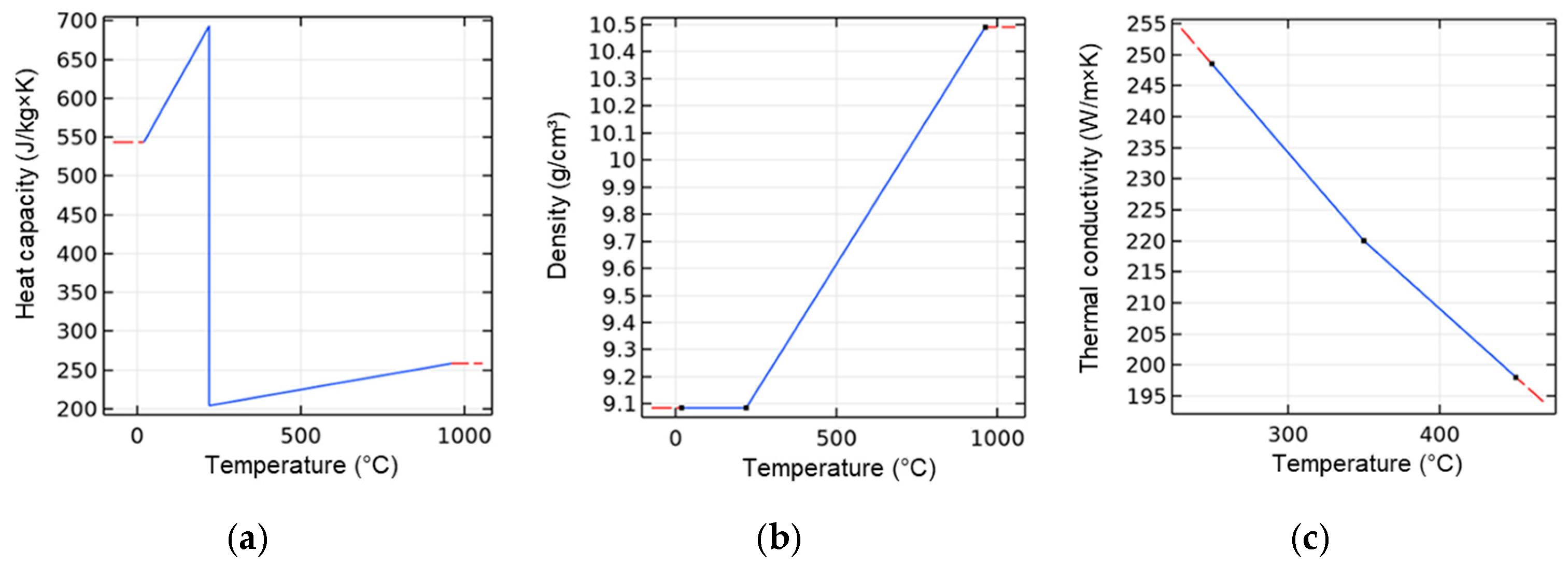
Figure 5 presents the associated modeled properties of heat capacity, density, and thermal conductivity as a function of temperature.
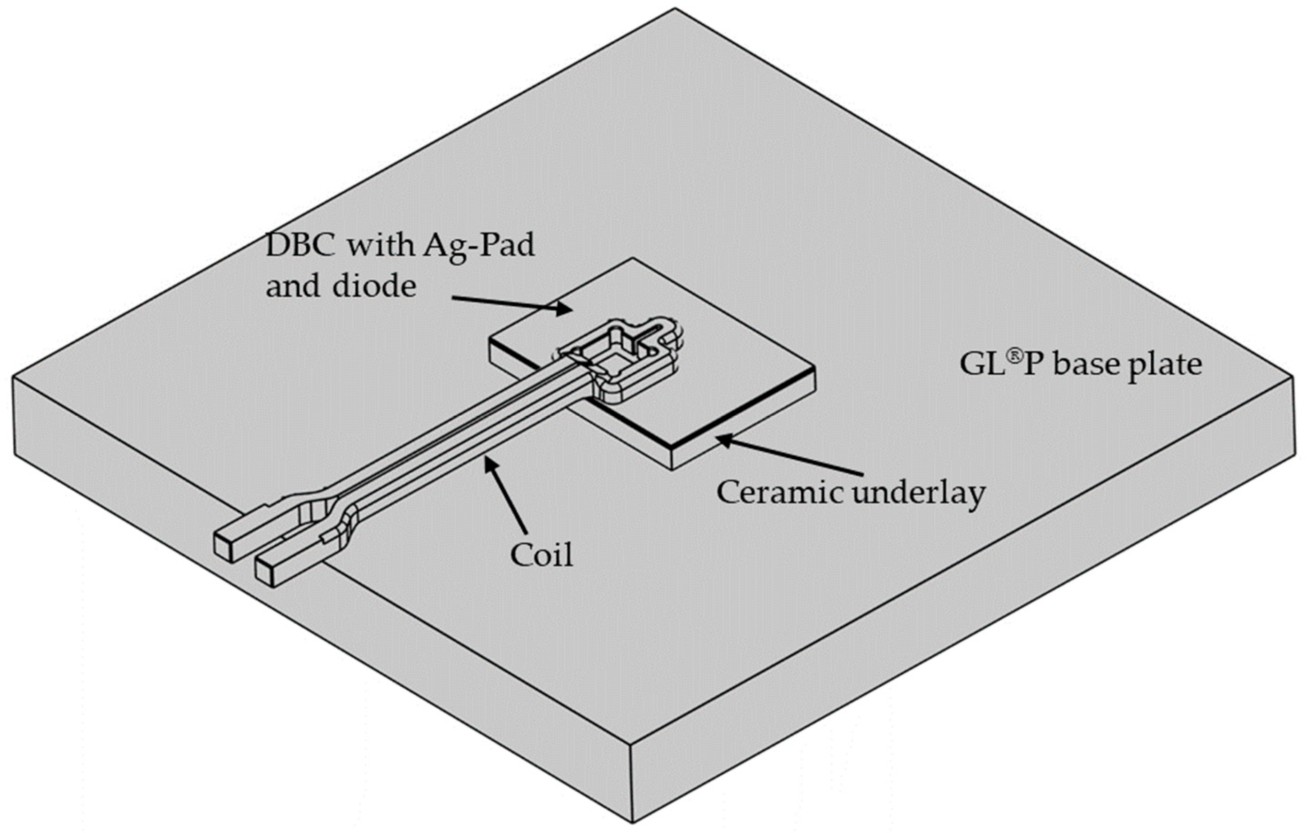
By using the simulation tools, it was possible to develop a suitable coil geometry for the single-chip bonding tests. The coil has a single convolution, which was subject to numerous iterative adjustments in design in order to focus the maximum heat input to the bonding area on the DBC substrate. As a result, good homogenization of the inductively generated heat could be realized, so that a uniform and selective heating of the bond zone is possible. An additional circular segment was realized in the rear part of the induction coil’s electric line, which allows for a Rogowski coil to be arranged at the coil, so that the current through the coil as well as the frequency of the alternating current could be measured in the experiments. A CAD image of the coil is shown in Figure 6.
The developed coil was first analyzed virtually regarding its suitability for inductive heating of the stack. Figure 7a demonstrates a coil current of I = 1280 A (peak-to-peak), a frequency of the electromagnetic field of f = 1022 kHz and a heating duration of th = 7.0 s. FE simulations showed that sufficient heating (Tsinter ≈ 230 °C) of the silver sintering pad can be realized. Areas of the DBC substrate that are below the coil convolution exhibit the highest temperatures, while temperatures decrease significantly with an increasing distance from the convolution. Figure 7b shows the surface temperature distribution within the silver-sinter layer in detail. The temperatures at this location are 206.0 ≤ T ≤ 263.1 [°C]. A hot spot with Tmax = 319.2 °C is located at the lower edge of the DBC substrate because of the induced current accumulating there due to the skin effect. As a result of thermal conductivity, the bottom edge of the silver pad also exhibits a hot spot, and the temperatures are decreasing significantly towards the silver pad top side. This temperature inhomogeneity (ΔT = 57.1 K) within the silver pad could be problematic with regard to the formation of a homogeneous microstructure in the bond layer. Further optimization of the coil shape is needed to reduce the temperature inhomogeneity to values below ΔT < 20.0 K, which is part of future investigations. Nevertheless, the temperatures in the bond zone are sufficiently high for the sintering reaction to take place. In addition, the peak temperatures in the bonding zone of Tmax = 263.1 °C are not critical concerning the temperature stability of the semiconductor devices, so that no damage to them is to be expected during the induction-based bonding process. The very short bonding times are also advantageous in terms of minimizing thermal stress in the diodes.
Furthermore, Figure 7c shows a cross-sectional image of the temperature distribution in the stack perpendicular to the stack surface. The corresponding cross-section layer is marked in Figure 7a. It can be observed that the temperatures in the silver pad are almost identical to the temperatures of the DBC top layer directly below the pad. This means that the DBC substrate is primarily heated by induction heating and the silver pad is heated by heat flux from the DBC. A pronounced inductive heating effect in the silver pad cannot be observed from the simulations. This is due to the small thickness of the pad which is hAg = 30 µm and the penetration depth δ of the magnetic field in silver at f = 2 MHz. The penetration depth of an electrical conducting material is defined as the distance from the material surface, in which the major part (≈63%) of the electromagnetic field is absorbed and transformed into heat. It is calculated by the formula
δ = 1 π · f · μ 0 · μ r · σ
In the formula, f is the frequency of the electromagnetic field, µ0 is the vacuum magnetic permeability, µr is the relative permeability, and σ is the electrical conductivity. For silver, at a frequency of f = 2 MHz, the penetration depth of the electromagnetic field is δAg ≈ 45 µm. Because the silver pad is thinner than the penetration depth, the silver pad is practically transparent for the electromagnetic field and no inductive heating of this layer occurs. This means that the heating behavior of the silver pad is dominated by the heating behavior of the DBC substrate, and no accelerated heating of the silver-sinter layer can be expected. However, it is still possible that the electromagnetic field has an impact on the sintering kinetics of the silver layer during the bonding process. The simulation results were verified by the experimentally acquired results from the heating tests, performed without the application of a bonding pressure (see Section 3.3).

3.2. Coil Manufacturing

The coil’s front part, including the convolution, was manufactured using 3D printing, while the electric connectors were made by manually forming hollow copper profiles. As a 3D printing method, selective laser melting (PROTIQ GmbH, Germany) was applied. Highly conductive copper powder was used for this purpose, which was selectively melted and compacted in the printing process. Thus, the printed coil had an electrical conductivity of about σCu = 50 MS/m at a density of ρCu = 8.82 g/cm3 [30], which is very close to the corresponding values of pure copper. Then, the coil and the electric connectors were joined by soldering, thus realizing the coil according to the design in Figure 6. In the next step, the coil was installed in the test rig. Figure 8 shows the manufactured coil as it was used for the experiments.

3.3. Heating Experiments

Heating experiments were carried out by heating the stack with the manufactured coil but without applying a bonding force. In the experiments, coil current ranges of 998 < I < 1434 [A] (peak-to-peak value), frequency ranges of 1020 < f < 1022 [kHz] and heating times of up to th = 10.0 s were applied. The coupling distance in each experiment was s1 = 1.0 mm. The selection of the process parameters was made with reference to the simulative investigations as described in Section 2.3. Temperature measurement of the sample’s surface was performed by means of a thermal camera. 
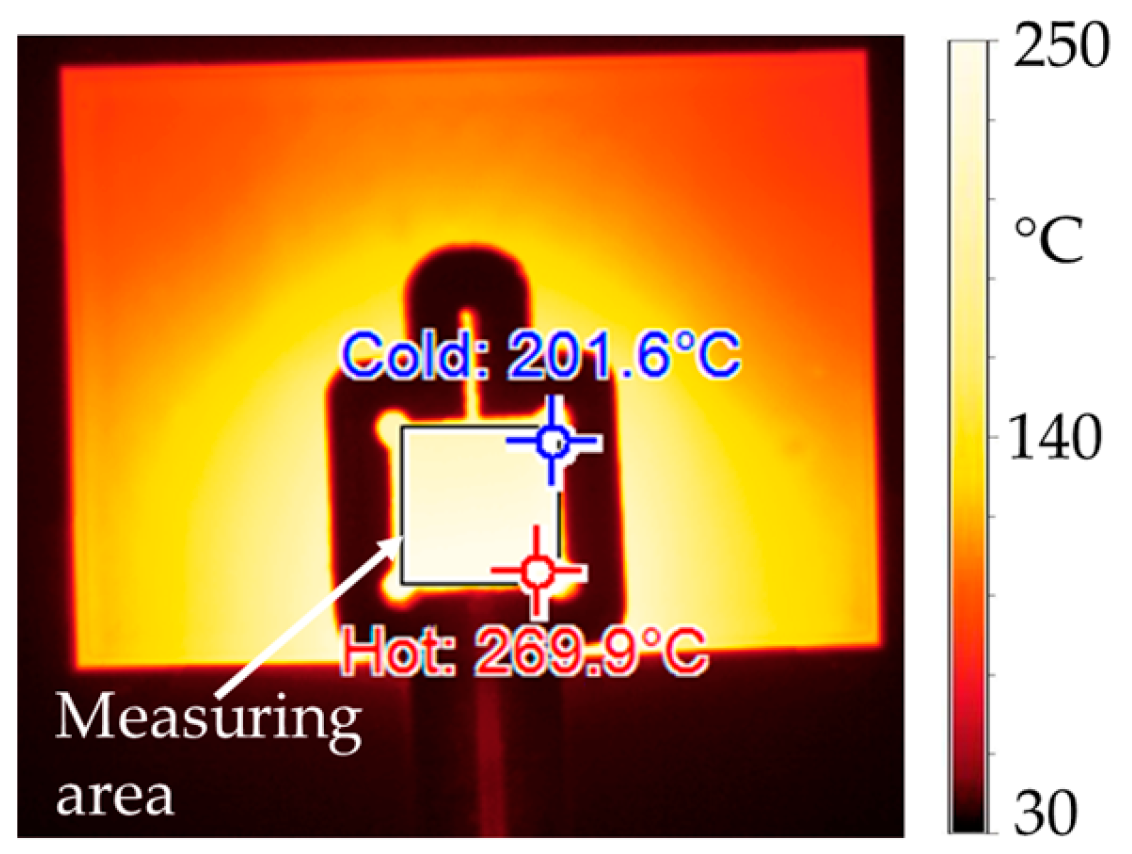
Figure 9 shows an exemplary thermal camera image of an inductively heated DBC substrate with a printed silver pad on it, which was captured during one of the heating tests. This temperature measurement method was used to determine characteristic temperature values in the bond zone and in the surrounding DBC substrate area. A diode was not placed on the pad during the heating tests.
From the measured temperatures, it can be observed that the hottest area is a wedge-shaped area inside or directly below the coil convolution. Thus, most of the heat is generated in the bond zone. Areas outside of the convolution are significantly less heated. It can be stated that the experimentally determined heating pattern largely matches the simulated one (Figure 7). For a more precise comparison of the results, the process parameters from Table 6 were used in the experiments and simulations, and the mean value of the surface temperature of the silver pad was measured and simulated, respectively. The resulting temperature-time graphs were plotted against each other as well as the absolute deviation of the temperature values. Figure 10 shows the corresponding diagrams.
The diagrams clearly indicate that there is very good match between the simulated and measured temperature values. The mean values of the temperature deviations are ΔTMV ≤ 5 K for all considered process parameter combinations. This suggests that the developed simulation model is robust and provides an accurate as well as a time- and space-resolved prediction of the temperatures in the stack in the investigated temperature range of 25 ≤ T ≤ 350 [°C]. In particular, larger deviations between the measured and simulated temperature values can be observed at the beginning of the heating process in the experiments in Figure 10a,b, as the initial temperature of Tstart = 25 °C selected as a boundary condition for all simulations could not be realized at the beginning of the experimental investigations.
For the simulation model, simplifications were made in order to reduce the complexity of the model: the porous structure of the silver-sinter layer was not taken into account and the thickness of the silver-sinter layer was defined as a constant. The water-cooled coil’s temperature was set to be constant at Tcoil = 20 °C but in reality, due to the small cross-section of the coil conductor and the resulting low volume flow rate of the cooling water, the cooling effect of the coil was expected to be lower than in the simulation. This could have an impact on the heating behavior of the inductive process. Finally, the model included no (thermo-) mechanical study step, which meant that no mechanical deformation of the geometric entities of the model was simulated due to the complex correlation of the bonding pressure, temperature, and thermo-mechanical properties of each component, as well as the intense volume change of the silver pad during the sintering process. Presumably, these factors have a huge impact on the sintering and heating behavior of the silver-sinter layer but are not taken into account in the simulation, which could be a source of significant deviations between simulated and experimentally determined temperature values. Instead, the simulation model was opted regarding the process parameters which were measured and validated through experimental trials. Despite the simplifications mentioned before, the model provided realistic results and allowed for a detailed pre-experimental process analysis by means of thermal analysis of the stack. The silver-sinter layer volume was very small in comparison to the DCB substrate and thus, the heating of the layer was dominated by the heating behavior of the DCB substrate. Finally, a more detailed modelling of the silver-sinter layer geometry and material properties is required in order to analyze the sintering kinetics on a phenomenological basis, which will be done in future investigations.

3.4. Sintering Experiments

In all test series according to Table 3, diodes were successfully bonded to DBC substrates with induction heating. The produced bonds were firm and of good quality. This proves that the induction technology is suitable for die bonding applications. After the initial visual inspection and manual strength testing of the samples, the bonds were characterized in depth by further analysis methods described in the following sections.

3.5. REM Analysis

Cross-sections of the bonded samples were prepared in order to conduct further investigations by means of SEM analysis. Sample preparation was performed as follows: First, the bonded diodes were cut out from the DBC substrate using waterjet cutting. After cutting, the samples were cold-embedded in epoxy resin. In the following grinding process, SiC papers with grain sizes from 120 to 2400 were used for wet grinding of the samples until the cut plane in the middle of the diode was reached. After grinding, the samples were polished using polishing cloth and diamond suspensions with grain sizes of 4 µm and 1 µm, respectively. After polishing, the samples were cleaned with ethanol and sample preparation was concluded.
In the following Figure 11, Figure 12 and Figure 13, an overview of the bonded samples is presented. In the figures, the stack’s cross-section consists of the three-layered DBC substrate (DBC-Cu, DBC-Al2O3, DBC-Cu), the silver-sinter layer and the diode (viewed from bottom to top). In each figure, four specimens from each test series (Table 3) are depicted. For the four samples of each test series, the bonding pressure and the generator power were kept constant, and the bonding time was varied. Because of the different bonding times, different maximum temperatures were reached at the end of the heating process. Maximum temperatures are noted in the figures.
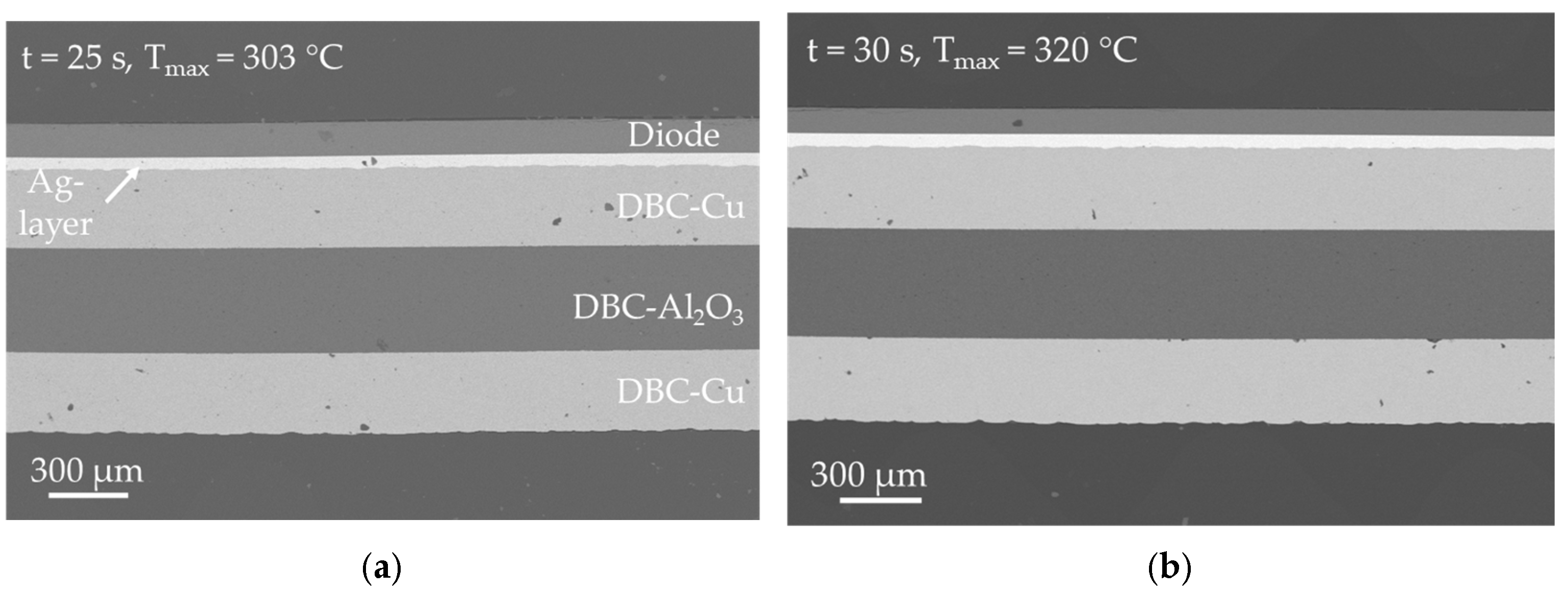
In Figure 11, SEM images of the samples, which were produced at a bonding pressure of p = 20.0 MPa (experimental series 1 in Table 3) are shown. This value was selected as starting point of investigation because a bonding pressure between 20.0 MPa ≤ p ≤ 30.0 MPa is common in current industrial silver sintering processes for die attach applications. The samples show a very good bonding between DBC substrate, silver layer and diode. The bond interface between the DBC substrate and silver-sintered layer as well as that between the diode and silver-sintered layer are free of defects or voids and the connection between the two components appears to be very firm. Likewise, the densification of the silver-sintered layer appears to be very high. Based on the images, no difference in densification of the layers can be observed as a result of the different bonding times or the measured maximum temperature. In addition, almost no defects were visible in the DBC layers which could be attributed to the bonding process. A few defects can be observed in the copper layers of the DBC substrates, especially in Figure 11c, but in terms of distribution and size, they do not allow any conclusion to be drawn about a bond process-related formation. Several cracks are visible on top of the diodes and are likely the result of the high bonding pressure and the direct contact between the ceramic punch and diode in the bonding process. The damage to the chips is particularly evident in Figure 11d.
Cross-sectional SEM pictures of the samples, which were produced with a bonding pressure of p = 10.0 MPa (experimental series 2 in Table 3), can be seen in Figure 12. From the images, an excellent bond between the DBC-Ag layer and the diode can be determined for all samples. The densification among all sintered layers in this figure is very high and can be compared to the samples from experimental series 1, which were produced at a bonding pressure of p = 20.0 MPa. In contrast, it is noticeable that a larger number of defects can be observed in the copper layers of the DBC substrate in the Figure 12a,b. Since the number of defects is much lower in Figure 12c,d, which is comprised of samples that were bonded for an even longer amount of time at almost the same temperature, it is assumed that these defects were already present in the DBC substrate before bonding. It is also possible that the sample was contaminated prior to the SEM analysis, and that the black dots are dust particles. Furthermore, a few cracks on the diode surface can be observed in Figure 12c. It is thus evident that the number of cracks is much lower in comparison to the samples that were bonded at p = 20.0 MPa. This demonstrates that a reduction of bonding pressure is beneficial with regard to production safety and quality. A more detailed analysis of the cracks is given later in this section.
SEM analysis of the samples in Figure 13 shows that a bonding pressure of p = 5 MPa is already sufficient to produce tight bonds between DBC substrate and diode. The morphology of the bond layers is identical to the previously analyzed samples and the bond to the diode as well as the DCB-Cu-layer is very well established. Several defects can be observed in Figure 10c at the interface between DBC-Al2O3 and the bottom DBC-Cu layer. However, these are presumably a result of the manufacturing process of the DBC substrate. Almost no cracks in the diode could be found for the samples bonded at p = 5 MPa.
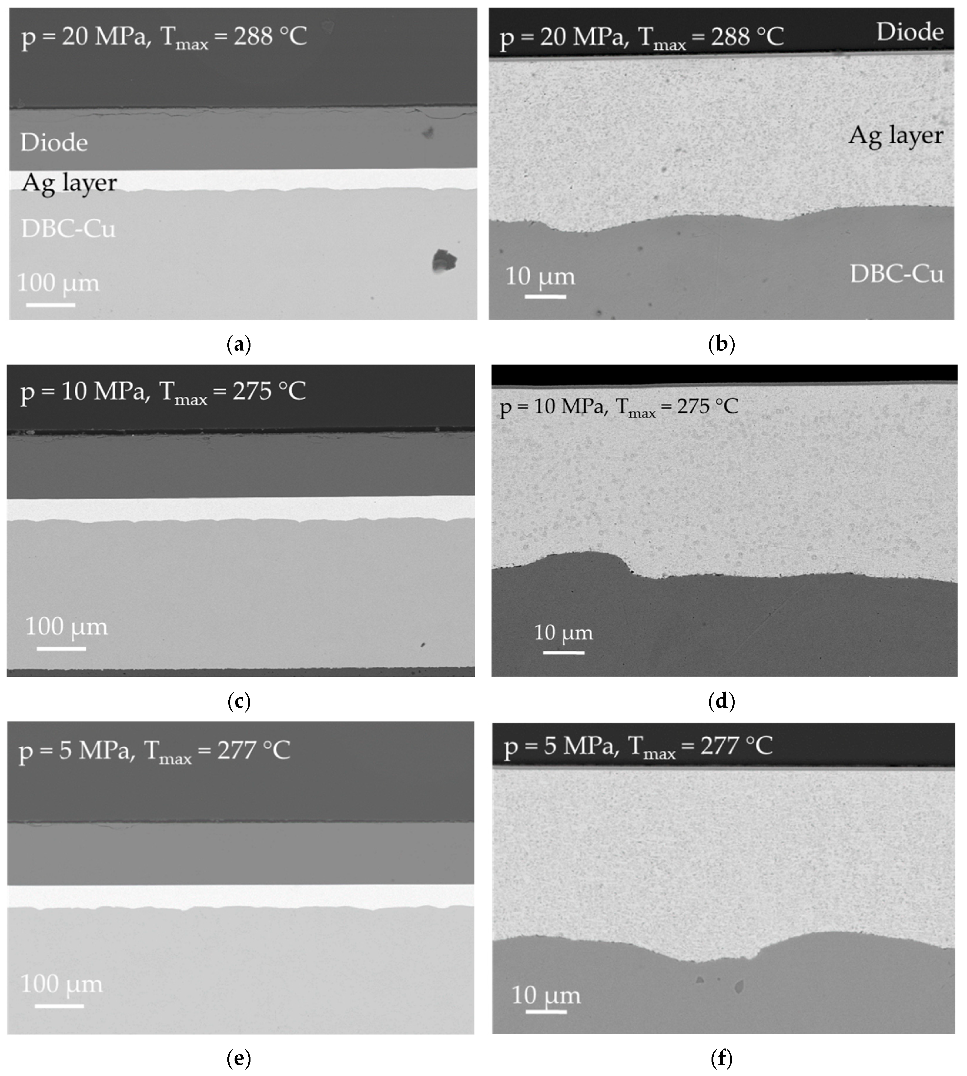
Figure 14 shows a more detailed analysis of the bond zone of the samples from all three experimental series that were bonded for t = 40.0 s according to Table 3. In Figure 14a,c,e, zoomed-in images of the layer system Diode-silver-DBC-Cu of the sample are shown. The samples were selected because the respective measured temperatures during the experiments were the lowest (t ≈ 280 °C) and thus closest to the desired bonding temperature of TS = 230 °C. As stated before, for all these samples a very good bonding between the diode and the silver-sinter layer can be observed. For all three samples, the thickness of the silver sintering layer is dAg = 44 µm. With regard to the morphology and microstructure of the three silver-sinter layers, they appear to be widely identical. However, for the samples bonded at p = 20.0 MPa (Figure 14a) and p = 10.0 MPa (Figure 14c), several cracks are visible on the diode’s top side, which is not the case for the sample bonded at p = 5.0 MPa (Figure 14e) where only a single, small crack can be observed. Therefore, a bonding pressure of p = 5.0 MPa is sufficient for inductive bonding with the silver-sinter paste. By applying this very low bonding pressure, strong and defect-free bonds can be produced and the risk of damage to the semiconductor components in the bonding process is reduced.
A detailed analysis of the silver-sinter layers of the samples is given in the SEM images in Figure 14b,d,f. It is clear that the densification is very high for all three samples. A certain residual porosity can be observed, but the overall structure and appearance of the layers is very homogeneous, as larger pores cannot be detected. Also, the investigations show that the temperature inhomogeneity during the heating process reported in Section 3.3 has no impact on the silver layer morphology, because all the investigated samples had an identical appearance throughout the cross-sections. A more precise quantitative analysis of layer porosity is to be carried out by means of focused ion beam (FIB) preparation and subsequent SEM analysis in future investigations. Additionally, the pictures prove that the interface between silver layer and diode is defect-free, and the two components are tightly bonded. With regard to the very low bonding times and pressures as well as the very high densification of the sintered silver layers, it can be assumed that there is a positive effect on the sintering of the particles with each other as well as to the DBC substrate and diode because of the inductive-heating method.
Furthermore, the detached sintered silver bars, which were previously examined by LaTIMA (Table 6), were subsequently analyzed by means of SEM. Figure 15 shows the SEM images of one LaTIMA sample for each annealing temperature. From the figures, it can be seen that the sample, which was thermally treated at T1 = 250 °C (Figure 15a), exhibits a clearly visible residual porosity, which is particularly pronounced in the upper and lower thirds of the layer. In the center, there is a comparatively dense zone with hardly any observable pores. However, the sample is already highly densified. The sintered sample, which was treated at T2 = 350 °C (Figure 15b), shows even less residual porosity, with a few pores primarily agglomerating in the upper third of the sample. Finally, Figure 15c shows that the sample, which was treated at T3 = 450 °C, no longer shows any visible pores. With increasing temperatures, a higher densification of the sintered structure can be observed, although a sufficiently high densification of the structure can already be observed at a sintering temperature of T1 = 250 °C.
In Section 3.1, the results of the LaTIMA investigations were discussed. For the discussed samples, a decrease in thermal conductivity with increases in the sintering temperature was observed, which was against expectations. With the recently presented SEM analyses of the detached silver-sinter layers, a more elaborated discussion of the results is possible. Generally, increasing the densification of a metallic sinter structure is accompanied by an increase in the thermal conductivity of a structure. The reason for this is that poorly sintered structures contain gas inclusions which have, compared to metals, lower thermal conductivity. Thus, as the densification of a sintered structure increases, the pore fraction decreases, and the thermal conductivity should also increase. This correlation was not true for the samples investigated in this paper. In order to explain this effect, the mean free path of gas molecules becomes important, which is defined as the average distance a molecule travels in a volume until it collides with another molecule and thus exchanges thermal energy. As the pores become smaller and reach nanoscale proportions (d < 100 nm) during the sintering process, the mean free path of the gas molecules is greater than the effective space (the pore) in which the gas molecule is confined. This leads to a significant decrease in the number of gas–molecule collisions during a constant time-period, and, consequently, to the strongly reduced thermal conductivity of gas in the pore. As a result, the overall thermal conductivity of the nano-porous sintered structure decreases. This effect is known as the Knudsen effect and can be used specifically to produce highly heat-insulating materials [31,32]. It is possible that this effect was also present in the sintered metallic structures studied here. As the densification of the silver-sinter layer progresses, the pores in it become smaller, but there is no complete densification of the sinter structure because there is no liquid metal that can enter the pores and seal them as the sintering process takes place without melting of the silver particles. Instead, the particles sinter only by solid-phase diffusion, so that a certain residual porosity remains even after a long period of sintering. Due to the very small dimensions of the pores, they are no longer visible in the SEM images in Figure 15a–c. However, the thermodynamic influence on the overall thermal conductivity can be clearly seen from the LaTIMA measurements. Since low thermal conductivity of the sintered layers is not desirable, this aspect of the sintering of silver particles during bonding requires further investigation and optimization.

3.6. Function Test

The results of the function tests by means of block-voltage measurement are shown in Table 7. The majority of the diodes survived the inductive bonding process without damage. For 10 out of 12 samples, an average leakage current of IL_MW = 271 nA was measured, which corresponds to failure-free functionality of the diodes. For sample diode 5, the measured leakage current was IL = 5000 nA. According to the measurement norm, this value is still below the limit for defective components (IL_crit = 25,000 nA), but it was notably high compared to the other samples. It is therefore assumed that this sample was also defective.
Diode sample 7, on the other hand, is clearly defective as a leakage current of IL = 30,000 nA was measured for it. With regard to the bonding-process parameters for this sample (Table 7), no correlation can be found between them and the cause of the damage. Neither the bonding time, nor the bonding pressure or the measured diode surface temperature during the bonding process were exceptional high. It is therefore unlikely that the thermal–electromagnetic stress on the diode in the bonding process led to the failure. For this reason, this sample was subjected to further optical microscopic investigations. The optical microscope analysis of the diode’s top metal revealed numerous damages (
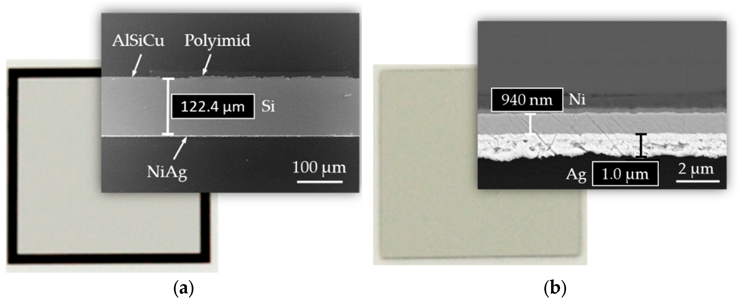
Figure 16a). In addition, the polyimide guarding at the frame of the diode was also damaged and deformed (Figure 16b). All these damages were presumably caused by the impact of the SiN punch on the diode surface during the bonding process. The mechanical impact of the punch on the diode surface presumably damaged the polyimide guarding to such an extent that functionally critical damage to the diode occurred.
Lock-in thermography is a non-destructive testing method for locating damaged areas of a defective diode. Figure 17a shows the results of the investigation for the sample diode 7 according to Table 7. In this test method, a pulse current is applied to the diode, and it is observed by means of a thermal camera. At the diode’s damaged locations, the leakage current flow is very high and as a result, the temperature increases significantly at these locations due to the Joule effect. During the investigations, a hot spot was detected on the right side of the sample diode. The optical microscopic analysis of the corresponding hotspot location is depictured in Figure 17b. There, a pit in the polyimide guarding can be clearly observed. As mentioned before, this pit was presumably caused by the mechanical impact of the SiN punch on the diode in the bonding process.
The results of the function test of the inductively bonded diodes showed that the inductive bonding process did not result in any damage to the semiconductor components. Instead, the observed damage could be attributed to the mechanical impact of the ceramic punch on the diodes’ surface. In future experiments, this problem will be overcome by technological adjustments to the test rig, for example by inserting a buffering polymer film between diode and ceramic punch. Therefore, there are no indications that the inductive bonding process itself caused any damage to the diodes. Furthermore, evidence has been provided that this technological approach is potentially suitable for industrial applications.

4. Conclusions

In this paper, an induction-heating technology with silver-sintering paste as an additive material were combined to bond semiconductor components firmly to DBC substrates within very short process times. In preliminary FE simulations, a valid simulation model was developed that allowed for a simulation of the inductive-heating process in terms of process analysis and tool optimization. With the aid of the model, it was possible to develop a coil geometry adapted to the geometry of the components to be bonded, which allowed for a focus on the heat input to the bond zone while ensuring that the surrounding area was less-affected by heat. Additionally, it was shown that a strong electromagnetic field does not damage the semiconductor components in the bonding process. SEM analyses of the bonded samples showed that excellent bonds could be established between the DBC substrate and the silver-sinter layer as well as between the silver-sinter layer and the diode. The bond interface showed virtually no defects; the bonds were firm and the sinter layers were highly densified. However, further optimizations are necessary with regard to the inductive-heating process in terms of coil geometry, position, and process parameters in order to ensure homogeneous temperatures in the bonding zone and to avoid hot and cold spots. The bonds need to be further analyzed by means of bond toughness, thermal fatigue resistance and ampacity in order to qualify the process for industrial large-scale production. Furthermore, the results of the investigations need to be transferred and qualified for multi-chip and substrate-bonding applications in further development steps.

Author Contributions

Conceptualization, P.R., C.H. and M.K.; methodology, P.R., C.H. and M.K.; validation, P.R.; formal analysis, P.R. and S.P.; investigation, P.R., S.P. and R.J.; data curation, P.R.; writing—original draft preparation, P.R. and C.H.; writing—review and editing, M.K. and K.H.; visualization, P.R. and C.H.; supervision, P.R.; project administration, P.R., C.H. and M.K.; funding acquisition, C.H., M.K. and K.H. All authors have read and agreed to the published version of the manuscript.

Funding

The research project was carried out in the framework of the industrial collective research program (IGF no. 20120 BR). It was supported by the Federal Ministry for Economic Affairs and Climate Action (BMWK) through the AiF (German Federation of Industrial Research Associations eV) based on a decision taken by the German Bundestag.

Data Availability Statement

Not applicable.

Conflicts of Interest

The authors declare no conflict of interest. The funders had no role in the design of the study; in the collection, analyses, or interpretation of data; in the writing of the manuscript; or in the decision to publish the results.

References

  1. Agarwal, S. Status of the Power Module Packaging Industry 2021—Market and Technology Report 2021; Yole Développement: Villeurbanne, France, 2021. [Google Scholar]
  2. Rössle, C.; Gottwald, T. Anforderungen an die Leistungselektronik, Teil 1. 2016. Available online: https://www.all-electronics.de/elektronik-fertigung/anforderungen-an-die-leistungselektronik-teil-1.html (accessed on 24 July 2023).
  3. Le Bret, C.; Zong, Z.; Grao Txapartegi, M.; Gueguen, P.; Lin, H.; Rosina, M. From Technologies to Market—Status of Power Electronics Industry 2016; Yole Développement: Villeurbanne, France, 2016. [Google Scholar]
  4. Dowling, N.E. Mechanical Behavior of Materials, 4th ed.; Angshuman Chakraborty: Essex, UK, 2013; ISBN 978-0-273-76455-7. [Google Scholar]
  5. Guth, K.; Siepe, D.; Görlich, J.; Torwesten, H.; Roth, R.; Hille, F.; Umbach, F. New assembly and interconnects beyond sintering methods. In Proceedings of the PCIM Europe 2010—New Assembly and Interconnect Technologies, Nuremberg, Germany, 4–6 May 2010. [Google Scholar]
  6. Yeom, J.; Nagao, S.; Chen, C.; Sugahara, T.; Zhang, H.; Choe, C.; Li, C.-F.; Suganuma, K. Ag particles for sinter bonding: Flakes or spheres? Appl. Phys. Lett. 2019, 114, 253103. [Google Scholar] [CrossRef]
  7. Yan, J. A Review of Sintering-Bonding Technology Using Ag Nanoparticles for Electronic Packaging. Nanomaterials 2021, 11, 927. [Google Scholar] [CrossRef] [PubMed]
  8. Peiner, E. Chipmontage mit Drucksintertechnik für Hochtemperaturanwendungen; Opening Ceremony Elsold GmbH & Co KG: Ilsenburg, Germay, 2013. [Google Scholar]
  9. Mertens, C. Die Niedertemperatur-Verbindungstechnik der Leistungselektronik; TU Braunschweig: Düsseldorf, Germay, 2004. [Google Scholar]
  10. Nikitin, I.; Pressel, K. Mechanical properties of porous silver materials depending on sintering parameters. In Proceedings of the 20th International Workshop on Thermal Investigations of ICs and Systems, Greenwich, UK, 24–26 September 2014; pp. 1–4. [Google Scholar] [CrossRef]
  11. Hutzler, A.; Tokarski, A.; Kraft, S.; Zischler, S.; Schletz, A. Increasing the lifetime of electronic packaging by higher temperatures: Solders vs. silver sintering. In Proceedings of the 2014 IEEE 64th Electronic Components and Technology Conference (ECTC), Orlando, FL, USA, 27–30 May 2014; pp. 1700–1706. [Google Scholar]
  12. Becker, M. Neue Technologien für hochzuverlässige Aufbau- und Verbindungstechniken Leistungselektronischer Bauteile; Technische Universität Chemnitz: Chemnitz, Germay, 2015. [Google Scholar]
  13. Lei, T.G.; Calata, J.N.; Lu, G.-Q.; Chen, X.; Luo, S. Low-Temperature Sintering of Nanoscale Silver Paste for Attaching Large-Area Chips. IEEE Trans. Components Packag. Technol. 2010, 33, 98–104. [Google Scholar] [CrossRef]
  14. Zou, G.; Yan, J.; Mu, F.; Wu, A.; Ren, J.; Hu, A. Low Temperature Bonding of Cu Metal through Sintering of Ag Nanoparticles for High Temperature Electronic Application. Open Surf. Sci. J. 2010, 3, 70–75. [Google Scholar] [CrossRef]
  15. Wang, M.; Mei, Y.; Hu, W.; Li, X.; Lu, G.-Q. Pressureless Sintered-Silver as Die Attachment for bonding Si and SiC Chips on Silver, Gold, Copper, and Nickel Metallization for Power Electronics Packaging: The Practice and Science. IEEE J. Emerg. Sel. Top. Power Electron. 2022, 10, 2645–2655. [Google Scholar] [CrossRef]
  16. Xiao, K.; Calata, J.N.; Zheng, H.; Ngo, K.D.T.; Lu, G.-Q. Simplification of the Nanosilver Sintering Process for Large-Area Semiconductor Chip Bonding: Reduction of Hot-Pressing Temperature Below 200 °C. IEEE Trans. Components Packag. Manuf. Technol. 2013, 3, 1271–1278. [Google Scholar] [CrossRef]
  17. Chew, L.M.; Stegmann, T.; Schwenk, E.; Dubis, M.; Schmitt, W. A new development of direct bonding to aluminum and nickel surfaces by silver sintering in air atmosphere. In Proceedings of the 2019 IEEE 69th Electronic Components and Technology Conference (ECTC), Las Vegas, NV, USA, 28–31 May 2019; pp. 87–93. [Google Scholar] [CrossRef]
  18. Zhao, Y.; Mumby-Croft, P.; Jones, S.; Dai, A.; Dou, Z.; Wang, Y.; Qin, F. Silver sintering die attach process for IGBT power module production. In Proceedings of the 2017 IEEE Applied Power Electronics Conference and Exposition (APEC), Tampa, FL, USA, 26–30 March 2017; pp. 3091–3094. [Google Scholar]
  19. Buttay, C.; Masson, A.; Li, J.; Johnson, M.; Lazar, M.; Raynaud, C. Die Attach of Power Devices Using Silver Sintering—Bonding Process Optimization and Characterization. In Proceedings of the HiTEN 2011, Oxford, UK, 17–18 July 2011; pp. 1–7. Available online: https://hal.archives-ouvertes.fr/hal-00672619/ (accessed on 24 July 2023).
  20. Sosnowchik, B.D.; Azevedo, R.G.; Myers, D.R.; Chan, M.W.; Pisano, A.P.; Lin, L. Rapid silicon-to-steel bonding by induction heating for MEMS strain sensors. J. Microelectromech. Syst. 2012, 21, 497–506. [Google Scholar] [CrossRef]
  21. Hofmann, C.; Baum, M.; Satwara, M.; Kroll, M.; Panhale, S.; Rochala, P.; Paul, S.-D.; Oi, K.; Murayama, K.; Wiemer, M.; et al. Silver sintering technology based on induction heating for chip level bonding. In Proceedings of the 2021 IEEE CPMT Symposium Japan (ICSJ), Kyoto, Japan, 10–12 November 2021; pp. 33–36. [Google Scholar]
  22. Rochala, P.; Hofmann, C.; Kroll, M.; Wiemer, M.; Kräusel, V. Chip-level bonding for microelectronic components by induction sintering of micro structured Ag particles. In Proceedings of the XIX International UIE Congress on Evolution and New Trends in Electrothermal Processes—UIE, Pilsen, Czech Republic, 1–3 September 2021. [Google Scholar]
  23. Yang, H.-A.; Lin, C.-W.; Peng, C.-Y.; Fang, W. On the selective magnetic induction heating of micron scale structures. J. Micromech. Microeng. 2006, 16, 1314–1320. [Google Scholar] [CrossRef] [Green Version]
  24. Hofmann, C.; Fröhlich, A.; Wiemer, M. A Novel Method for MEMS Wafer-Level Packaging: Selective and Rapid Induction Heating for Copper-Tin SLID Bonding. In Proceedings of the 2019 20th International Conference on Solid-State Sensors, Actuators and Microsystems & Eurosensors XXXIII (TRANSDUCERS & EUROSENSORS XXXIII), Berlin, Germany, 23–27 June 2019; Volume 20, p. 4. [Google Scholar]
  25. Hofmann, C.; Satwara, M.; Kroll, M.; Panhale, S.; Rochala, P.; Wiemer, M.; Hiller, K.; Kuhn, H. Localized Induction Heating of Cu-Sn Layers for Rapid Solid-Liquid Interdiffusion Bonding Based on Miniaturized Coils. Micromachines 2022, 13, 1307. [Google Scholar] [CrossRef] [PubMed]
  26. Guyon, A.; Biguereau, E.; Bouvard, D.; Chaix, J.-M.; Roure, S. Direct Induction Sintering of Nickel and Silver Powders. In Proceedings of the World PM2016 Proceedings: Congress Centre Hamburg (CCH), Hamburg, Germany, 9–13 October 2016; European Powder Metallurgy Association (EPMA): Shrewsbury, UK, 2016; p. 6. [Google Scholar]
  27. Arnold, H. Induktives Chip-Bonden: Innovationssprung für die Leistungselektronik. 2022. Available online: https://www.elektroniknet.de/elektronikfertigung/fertigungstechnik/innovationssprung-fuer-die-leistungselektronik.193922.html (accessed on 24 July 2023).
  28. Olevsky, E.A.; Dudina, D. V Field-Assisted Sintering; Springer International Publishing: Cham, Switzerland, 2018; ISBN 978-3-319-76031-5. [Google Scholar]
  29. Markin, A.V.; Smirnova, N.N.; Il’ichev, I.S.; Dolinsky, T.I.; Radbil, A.B. Thermodynamic properties of α-terpineol over the range from T → (0 to 345) K. J. Therm. Anal. Calorim. 2016, 123, 1451–1458. [Google Scholar] [CrossRef]
  30. PROTIQ Web Page. Available online: https://www.protiq.com/ (accessed on 24 July 2023).
  31. Merillas, B.; Vareda, J.P.; Martín-de León, J.; Rodríguez-Pérez, M.Á.; Durães, L. Thermal Conductivity of Nanoporous Materials: Where Is the Limit? Polymers 2022, 14, 2556. [Google Scholar] [CrossRef] [PubMed]
  32. Smith, D.S.; Alzina, A.; Bourret, J.; Nait-Ali, B.; Pennec, F.; Tessier-Doyen, N.; Otsu, K.; Matsubara, H.; Elser, P.; Gonzenbach, U.T. Thermal conductivity of porous materials. J. Mater. Res. 2013, 28, 2260–2272. [Google Scholar] [CrossRef] [Green Version]
Figure 1. Diode before chip bonding: (a) photographic image and SEM cross-section of the whole diode; and (b) photographic image and detailed SEM cross-section image of the back side.
Electronics 12 03247 g001
Figure 2. DBC substrate before chip bonding: (a) photographic image of the copper-metallized bond surface; and (b) SEM cross-sectional image of the DBC Cu-Al2O3-Cu layer system.
Electronics 12 03247 g002
Figure 3. Geometric model of simulation (air box hidden).
Electronics 12 03247 g003
Figure 4. Photographic images of the experimental inductive test rig: (a) entire system with each important component; and (b) sintering chamber with support plate for the DBC substrate.
Electronics 12 03247 g004
Figure 5. Temperature-dependent parameters of the particle paste ASP 043-04 used in the simulation: (a) heat capacity; (b) density; and (c) thermal conductivity.
Electronics 12 03247 g005
Figure 6. CAD image of the final coil design. Right side: detail of the convolution.
Electronics 12 03247 g006
Figure 7. Simulated surface temperature distribution of (a) the stack and (b) of the silver-sinter layer. (c) Simulated temperature distribution in the cross-section of the stack marked with “A” in image (a) and zoomed-in cross-section of silver pad. Color legend in (a) valid for all three images. Process parameters: coil current I = 1280 A (peak-to-peak), frequency of the electromagnetic field f = 1022 kHz, and heating time th = 7 s.
Electronics 12 03247 g007
Figure 8. The manufactured coil after simulative optimization.
Electronics 12 03247 g008
Figure 9. Thermal camera image captured during the pressureless inductive heating (frequency of electromagnetic field f = 1022 kHz, current through coil I = 1280 A, heating time t = 7.0 s) of a DBC with a printed and pre-dried silver pad. The measuring area corresponds to the position of the diode during the sintering experiments.
Electronics 12 03247 g009
Figure 10. Temperature-time-plots for the silver sinter pad surface from simulation and experiment: process parameters used for the test series (ad) according to Table 6.
Electronics 12 03247 g010
Figure 11. SEM-BSE analysis of the specimens inductively bonded for (a) 25 s, (b) 30 s, (c) 40 s and (d) 50 s according to experimental series 3 in Table 3. A bonding pressure of p = 20.0 MPa was applied to each specimen. The frequency of the electromagnetic field was f ≈ 1024 kHz in each case.
Electronics 12 03247 g011
Figure 12. SEM-BSE analysis of the specimens inductively bonded for (a) 25 s, (b) 30 s, (c) 40 s and (d) 50 s according to experimental series 3 in Table 3. A bonding pressure of p = 10.0 MPa was applied to each specimen. The frequency of the electromagnetic field was f ≈ 1023 kHz in each case.
Electronics 12 03247 g012aElectronics 12 03247 g012b
Figure 13. SEM-BSE analysis of the specimens inductively bonded for (a) 25 s, (b) 30 s, (c) 40 s and (d) 50 s according to experimental series 3 in Table 3. A bonding pressure of p = 5.0 MPa was applied to each specimen. The frequency of the electromagnetic field was f ≈ 1022 kHz in each case.
Electronics 12 03247 g013
Figure 14. (a,b): zoomed-in SEM image of sample in Figure 11c. (c,d): zoomed-in SEM image of sample in Figure 12c. (e,f): zoomed-in SEM image of sample in Figure 13c. Bonding time and frequency of the electromagnetic field were t = 40.0 s and f ≈ 1023 kHz, respectively, for all three samples.
Electronics 12 03247 g014
Figure 15. SEM analysis of the detached silver-sinter layers thermally treated at different temperatures and analyzed by LaTIMA method according to Table 4: (a) sample 2 in Table 4, sintered at T1 = 250 °C; (b) sample 4 in Table 4, sintered at T2 = 350 °C; and (c) sample 6 in Table 4, sintered at T3 = 450 °C.
Electronics 12 03247 g015
Figure 16. Optical microscope image of sample diode 7 (see Table 7) after bonding: (a) scratches and abrasions on the top metal side of the diode; and (b) traces of mechanical influence on the polyimide guarding of the diode.
Electronics 12 03247 g016
Figure 17. Further analysis of sample diode 7 from Table 7: (a) lock-in thermography of the diode in order to localize the leakage current flow; and (b) optical microscope image of the hot spot area.
Electronics 12 03247 g017
Table 1. Material and design parameters of the bond substrates.
SymbolUnitValue
Diode
LengthlDmm9.0
WidthwDmm9.0
ThicknessdDµm120.0
Bond metallization: Thickness NidNiµmapprox. 1
Bond metallization: Thickness AgdAgµmapprox. 1
DBC substrate
LengthlDmm53.0
WidthwDmm39.0
Thickness aluminum oxidehAl2O3µmapprox. 400.0
Thickness copperhCuµmapprox. 300.0
Ag paste pad
Pad lengthlAgmm10.0
Pad widthwAgmm10.0
Pad thickness after pre-dryinghAg_صm28.6
Ag particle diameterDAgµm≤20
Silver contentVAgwt%85.0
Table 2. Material parameters for the FEM. T represents the temperature for temperature-transient values with cAir = 1047.64 − 0.37 × T + 9.45 × 10⁻⁴ × T2 − 6.02 × 10⁻⁷ × T3 + 1.29 × 10⁻¹⁰ × T4 and λAir = −0.00227583562 + 1.15 × 10⁻⁴ × T − 7.90 × 10⁻⁸ × T2 + 4.12 × 10⁻¹¹ × T3 − 7.44 × 10⁻¹⁵ × T4.
MaterialProperty
Rel. Permeability μDielectric Constant εr
Air1.01.0
Al2O31.09.8
Si (Diode)1.011.7
Cu1.01.0
GL®P1.01.0
SiN1.07.5
El. Conductivity σ [S/m]Heat capacity c [J/(kg∙K)]
Air1.0cAir
Al2O310−18900
Si (Diode)6.4 × 10−2700
Cu5.998 × 107385
GL®P10−151140
SiN0.0760
Th. Conductivity λ [W/(m∙K)]Density ϱ [g/cm3]
AirλAirϱAir
Al2O3273.9
Si (Diode)1302.329
Cu4008.94
GL®P0.372.1
SiN21.53.17
Reference resistivity ρ
@ 293.15 K [Ω∙m]
Resistance coefficient K [1/K]
Cu1.667 × 10−83.862 × 10⁻³
Table 3. Overview of process parameters for three experimental bonding series.
ParameterExperimental Series
123
Coupling distance coil—DBC [mm]1.01.01.0
Heating time [s]25; 30; 40; 5025; 30; 40; 5025; 30; 40; 50
Max. Frequency [kHz]102410241024
Current range (peak-peak) [A]1292–14581287–14591290–1465
Joining pressure [MPa]20.010.05.0
Table 4. Annealing temperature, measured thickness, and heat conductivity λ after annealing of the silver sintering bars.
SampleAnnealing Temp. [°C]Thickness after Sintering [µm]Thermal Conductivity λ [W/mK]Δλ [W/mK]
125017725026
225017124738
335020422230
435022621836
545021519727
645019519928
Table 5. Material properties of the silver sinter paste ASP 043-04 for the FE simulation.
Material PropertySymbolUnitValue
Relative permeabilityμ-0.999975
Dielectric constantεr-7
Reference resistivity @ 298.15 KρΩ∙m1.6 × 10−5
Resistance coefficientK1/K3.8 × 10−3
Table 6. Process parameters of the five test series conducted for verification of the simulation and experiment. ΔTMV: mean value of the temperature deviation between simulation and experiment. ΔTStD: standard deviation of ΔTMV.
Test SeriesProcess ParameterΔTMV [K]ΔTStD [K]
Iind (Peak-Peak) [A]f [kHz]th [s]
(a)1140102110.0−4.894.54
(b)1280102210.03.623.97
(c)1296102210.01.281.91
(d)1434102210.02.295.21
Table 7. Process parameters and results of leakage current measurement of the investigated bonded diodes. Frequency of the electromagnetic field for all samples was f ≈ 1022 kHz, coupling distance between coil and DBC surface d = 1.0 mm.
SampleBond Time [s]Bonding Pressure [MPa]Max. Diode Surface Temp. [°C]Leakage Current [nA]Evaluation
125.05.0312275OK
230.05.0318270OK
340.05.0277270OK
450.05.0311250OK
525.010.03035000Leakage current OK but exceptional high value
630.010.0320280OK
740.010.027530,000not OK
850.010.0306280OK
925.020.0314250OK
1030.020.0318300OK
1140.020.0288255OK
1250.020.0321280OK
Disclaimer/Publisher’s Note: The statements, opinions and data contained in all publications are solely those of the individual author(s) and contributor(s) and not of MDPI and/or the editor(s). MDPI and/or the editor(s) disclaim responsibility for any injury to people or property resulting from any ideas, methods, instructions or products referred to in the content.

