New Methodology for Parasitic Resistance Extraction and Capacitance Correction in RF AlGaN/GaN High Electron Mobility Transistors
Abstract
1. Introduction
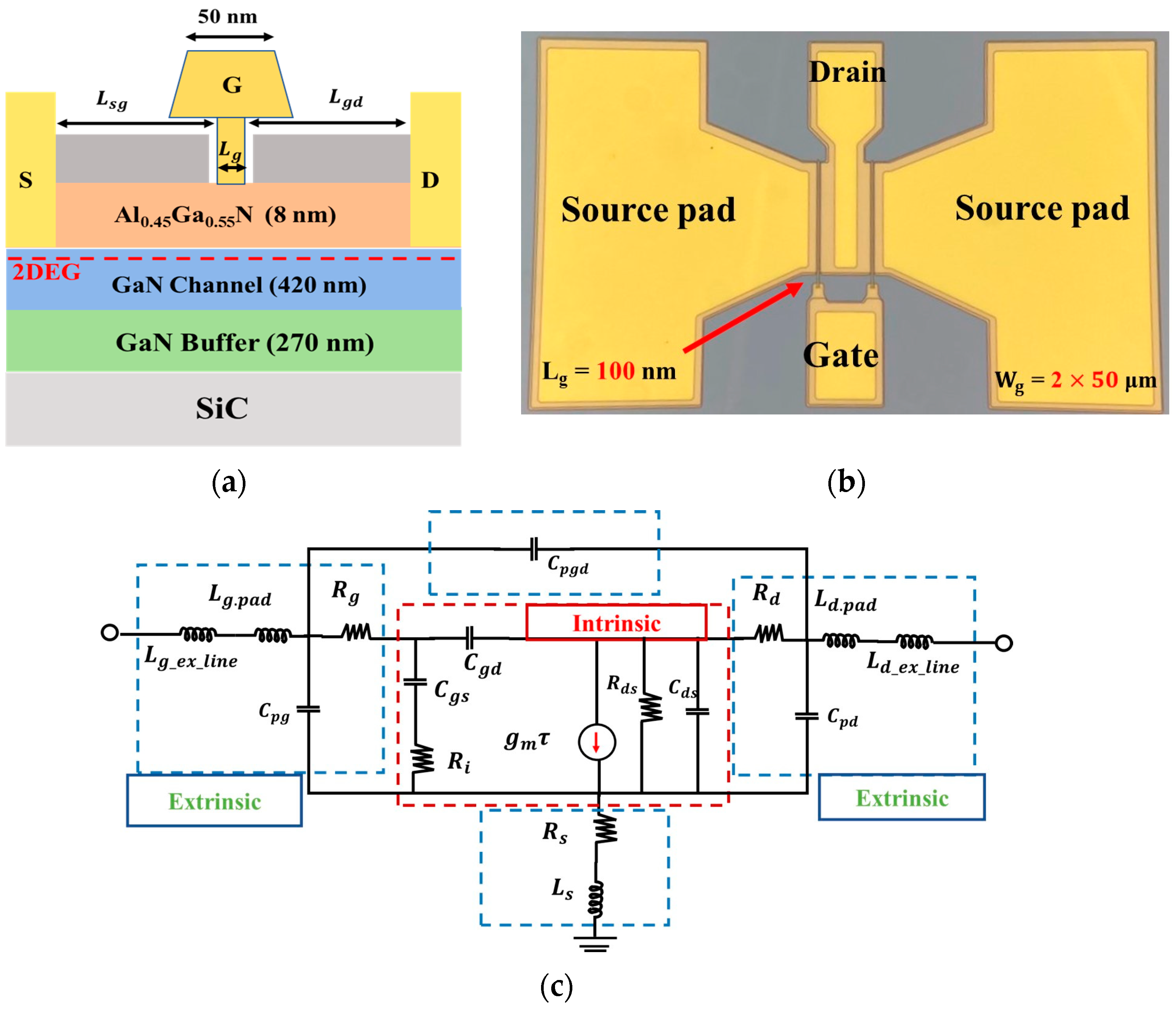
2. Materials and Measurement of the Equivalent Circuit
2.1. Fabrication
2.2. Problem Statement
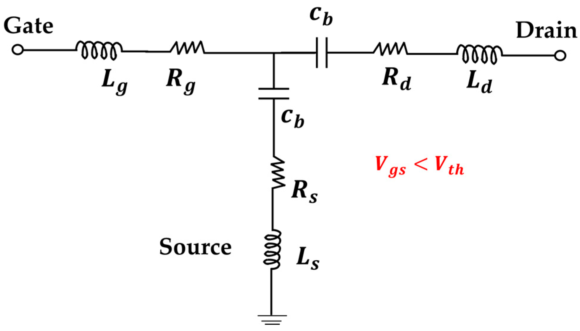
2.3. New Method of Resistance Extraction
3. Results and Discussion
3.1. Resistance Extraction from Cold-FET
3.2. Parasitic Capacitance Extraction by Dambrine’s Model
3.3. Model and Measurement Data Validation
4. Conclusions
Author Contributions
Funding
Data Availability Statement
Conflicts of Interest
References
- Mishra, U.K.; Shen, L.; Kazior, T.E.; Wu, Y.F. GaN-based RF power devices and amplifiers. Proc. IEEE 2008, 96, 287–305. [Google Scholar] [CrossRef]
- Chakraborty, S.; Kim, T.W. Investigation of mean-time-to-failure measurements from AlGaN/GaN high-electron-mobility transistors using Eyring model. Electronics 2021, 10, 3052. [Google Scholar] [CrossRef]
- Chakraborty, S.; Kim, T.W. Comprehensive Schottky Barrier Height Behavior and Reliability Instability with Ni/Au and Pt/Ti/Pt/Au on AlGaN/GaN High-Electron-Mobility Transistors. Micromachines 2022, 13, 84. [Google Scholar] [CrossRef] [PubMed]
- Amir, W.; Shin, J.W.; Shin, K.Y.; Kim, J.M.; Cho, C.Y.; Park, K.H.; Hoshi, T.; Tsutsumi, T.; Sugiyama, H.; Matsuzaki, H.; et al. A quantitative approach for trap analysis between Al0.25Ga0.75N and GaN in high electron mobility transistors. Sci. Rep. 2021, 11, 22401. [Google Scholar] [CrossRef]
- Chakraborty, S.; Amir, W.; Shin, J.W.; Shin, K.Y.; Cho, C.Y.; Kim, J.M.; Hoshi, T.; Tsutsumi, T.; Sugiyama, H.; Matsuzaki, H.; et al. Explicit Thermal Resistance Model of Self-Heating Effects of AlGaN/GaN HEMTs with Linear and Non-Linear Thermal Conductivity. Materials 2022, 15, 8415. [Google Scholar] [CrossRef] [PubMed]
- Shin, K.-Y.; Shin, J.-W.; Chakraborty, S.; Amir, W.; Shin, C.-S.; Kim, T.-W. Trap Behavior of Metamorphic HEMTs with Pulsed IV and 1/f Noise Measurement. In Proceedings of the ESSDERC 2022—IEEE 52nd European Solid-State Device Research Conference (ESSDERC), Milan, Italy, 19–22 September 2022; pp. 324–327. [Google Scholar] [CrossRef]
- Caddemi, A.; Crupi, G.; Donato, N. A robust and fast procedure for the determination of the small signal equivalent circuit of HEMTs. Microelectron. J. 2004, 35, 431–436. [Google Scholar] [CrossRef]
- Dambrine, G.; Cappy, A.; Heliodore, F.; Playez, E. A new method for determining the FET small-signal equivalent circuit. IEEE Trans. Microw. Theory Tech. 1988, 36, 1151–1159. [Google Scholar] [CrossRef]
- Amir, W.; Shin, J.; Shin, K.; Chakraborty, S.; Cho, C.; Kim, J.; Lee, S.; Hoshi, T.; Tsutsumi, T.; Sugiyama, H.; et al. Performance Enhancement of AlGaN/GaN HEMT via Trap-State Improvement. IEEE Trans. Electron Devices 2023, 170, 2988–2993. [Google Scholar] [CrossRef]
- Amir, W.; Chakraborty, S.; Kwon, H.-M.; Kim, T.-W. Impact of Charge-Trapping Effects on Reliability Instability in AlxGa1−xN/GaN High-Electron-Mobility Transistors with Various Al Compositions. Materials 2023, 16, 4469. [Google Scholar] [CrossRef]
- Amir, W.; Shin, J.W.; Chakraborty, S.; Shin, K.Y.; Hoshi, T.; Tsutsumi, T.; Sugiyama, H.; Kwon, H.M.; Kim, T.W. Instability Assessment of AlGaN/GaN High Electron Mobility Transistors Under High Drain Current Condition. In Proceedings of the Asia-Pacific Microwave Conference (APMC 2022), Yokohama, Japan, 29 November–2 December 2022; pp. 184–186. [Google Scholar]
- Cuerdo, R.; Calle, F.; Braña, A.F.; Cordier, Y.; Azize, M.; Baron, N.; Chenot, S.; Muñoz, E. High temperature behaviour of GaN HEMT devices on Si(111) and sapphire substrates. Phys. Status Solidi C 2008, 5, 1971–1973. [Google Scholar] [CrossRef]
- Tan, W.; Uren, M.; Fry, P.; Houston, P.; Balmer, R.; Martin, T. High temperature performance of AlGaN/GaN HEMTs on Si substrates. Solid-State Electron. 2006, 50, 511–513. [Google Scholar] [CrossRef]
- Crupi, G.; Xiao, D.; Schreurs, D.M.M.P.; Limiti, E.; Caddemi, A.; De Raedt, W.; Germain, M. Accurate multibias equivalent-circuit extraction for GaN HEMTs. IEEE Trans. Microw. Theory Tech. 2006, 54, 3616–3621. [Google Scholar] [CrossRef]
- Vandamme, E.P.; Schreurs, D.M.M.P.; Van Dinther, C. Improved three-step de-embedding method to accurately account for the influence of pad parasitics in silicon on-wafer RF test-structures. IEEE Trans. Electron Devices 2001, 48, 737–742. [Google Scholar] [CrossRef]
- Tiemeijer, L.F.; Havens, R.J.; Jansman, A.B.M.; Bouttement, Y. Comparison of the “Pad-Open-Short” and for Accurate On-Wafer RF Characterization of High-Quality Passives. IEEE Trans. Microw. Theory Tech. 2005, 53, 723–729. [Google Scholar] [CrossRef]
- Cho, H.; Burk, D. A three-step method for the de-embedding of high-frequency S-parameter measurements. IEEE Trans. Electron Devices 1991, 38, 1371–1375. [Google Scholar] [CrossRef]
- Koolen, M.C.A.M.; Geelen, J.A.M.; Versleijen, M.P.J.G. An improved de-embedding technique for on-wafer high-frequency characterization. In Proceedings of the 1991 Bipolar Circuits and Technology Meeting, Minneapolis, MN, USA, 9–10 September 1991; pp. 188–191. [Google Scholar] [CrossRef]
- Bazzi, J.; Kassem, H.; Curutchet, A.; Pourchon, F.; Derrier, N.; Celi, D.; Zimmer, T. A two-step de-embedding method valid up to 110 GHz. In Proceedings of the 2017 29th International Conference on Microelectronics (ICM), Beirut, Lebanon, 10–13 December 2017; pp. 1–4. [Google Scholar] [CrossRef]
- Kolding, T.E. A four-step method for de-embedding gigahertz on-wafer CMOS measurements. IEEE Trans. Electron Devices 2000, 47, 734–740. [Google Scholar] [CrossRef]
- Luo, J.; Zhang, L.; Wang, Y. A Distributed De-Embedding Solution for CMOS mm-Wave On-Wafer Measurements Based-on Double Open-Short Technique. IEEE Microw. Wirel. Compon. Lett. 2013, 23, 686–688. [Google Scholar] [CrossRef]
- Zhang, B.; Xiong, Y.-Z.; Wang, L.; Hu, S.; Li, J.L.-W. On the De-Embedding Issue of Millimeter-Wave and Sub-Millimeter-Wave Measurement and Circuit Design. IEEE Trans. Compon. Packag. Manuf. Technol. 2012, 2, 1361–1369. [Google Scholar] [CrossRef]
- Yau, K.H.K.; Sarkas, I.; Tomkins, A.; Chevalier, P.; Voinigescu, S.P. On-wafer S-parameter de-embedding of silicon active and passive devices up to 170 GHz. In Proceedings of the 2010 IEEE MTT-S International Microwave Symposium, Anaheim, CA, USA, 23–28 May 2010; pp. 600–603. [Google Scholar] [CrossRef]
- White, P.M.; Healy, R.M. Improved equivalent circuit for determination of MESFET and HEMT parasitic capacitances from ‘coldfet’ measurements. IEEE Microw. Guid. Wave Lett. 1993, 3, 453–454. [Google Scholar] [CrossRef]
- Yang, C.K.; Roblin, P.; De Groote, F.; A Ringel, S.; Rajan, S.; Teyssier, J.P.; Poblenz, C.; Pei, Y.; Speck, J.; Mishra, U.K. Pulsed-IV Pulsed-RF Cold-FET Parasitic Extraction of Biased AlGaN/GaN HEMTs Using Large Signal Network Analyzer. IEEE Trans. Microw. Theory Tech. 2010, 58, 1077–1088. [Google Scholar] [CrossRef]
- Zhang, H.; Ma, P.; Lu, Y.; Zhao, B.; Zheng, J.; Ma, X.; Hao, Y. Extraction method for parasitic capacitances and inductances of HEMT models. Solid-State Electron. 2017, 129, 108–113. [Google Scholar] [CrossRef]
- Kim, J. A New GaN HEMT Small-Signal Model Considering Source via Effects for 5G Millimeter-Wave Power Amplifier Design. Appl. Sci. 2021, 11, 9120. [Google Scholar] [CrossRef]
- Lu, J.; Wang, Y.; Ma, L.; Yu, Z. A new small-signal modeling and extraction method in AlGaN/GaN HEMTs. Solid-State. Electron. 2008, 52, 115–120. [Google Scholar] [CrossRef]
- Fukui, H. Determination of the Basic Device Parameters of a GaAs MESFET. Bell Syst. Tech. J. 1979, 58, 771–797. [Google Scholar] [CrossRef]
- Lee, K.W.; Lee, K.; Shur, M.S.; Vu, T.T.; Roberts, P.C.T.; Helix, M.J. Source drain and gate series resistance and electron saturation velocity in ion implanted GaAs FETs. IEEE Trans. Electron Devices 1985, 32, 5–10. [Google Scholar] [CrossRef]
- Byun, Y.H.; Shur, M.S.; Peczalski, A.; Schuermeyer, F.L. Gate-Voltage Dependence of Source and Drain Series Resistances and Effective Gate Length in GaAs MESFET’s. IEEE Trans. Electron Devices 1988, 35, 1241–1246. [Google Scholar] [CrossRef]
- Jarndal, A.; Kompa, G. A new small-signal modeling approach applied to GaN devices. IEEE Trans. Microw. Theory Tech. 2005, 53, 3440–3448. [Google Scholar] [CrossRef]


| Frequency | Rs (Ω) | Rd (Ω) | Rg (Ω) | Rch (Ω) |
|---|---|---|---|---|
| 20 GHz | 3.95 | 7.9 | 18.12 | 3.52 |
| 25 GHz | 1.89 | 3.78 | 16.89 | 7.3 |
| 30 GHz | 2.63 | 5.26 | 16.47 | 4.52 |
| 35 GHz | 3.18 | 6.35 | 15.25 | 1.66 |
| 40 GHz | 1.44 | 2.88 | 14.27 | 5.14 |
| Average | 2.62 | 5.23 | 16.20 | 4.42 |
| Frequency | Rs (Ω) | Rd (Ω) | Rg (Ω) | Rch (Ω) |
|---|---|---|---|---|
| 20 GHz | 1.29 | 2.58 | 14.47 | 13.90 |
| 25 GHz | 0.87 | 1.74 | 14.04 | 14.74 |
| 30 GHz | 0.98 | 1.96 | 13.49 | 14.08 |
| 35 GHz | 1.06 | 2.12 | 13.17 | 13.60 |
| 40 GHz | 0.80 | 1.60 | 12.77 | 13.98 |
| Average | 1.00 | 2.00 | 13.58 | 14.06 |
| Frequency | Rs (Ω) | Rd (Ω) | Rg (Ω) | Rch (Ω) |
|---|---|---|---|---|
| 20 GHz | 1.26 | 2.52 | 29.54 | 13.16 |
| 25 GHz | 1.02 | 2.04 | 24.32 | 13.48 |
| 30 GHz | 1.12 | 2.24 | 20.51 | 12.88 |
| 35 GHz | 1.22 | 2.44 | 18.25 | 12.32 |
| 40 GHz | 1.06 | 2.12 | 16.79 | 12.42 |
| Average | 1.14 | 2.27 | 21.88 | 12.85 |
| Parameters | Dambrine’s Model | Proposed Model |
|---|---|---|
| Cpg (fF) | 0.88 | 0.58 |
| Cpd (fF) | 16.7 | 1.19 |
| Extrinsic/Intrinsic | Model Parameters | Extracted Values | Extracted Values |
|---|---|---|---|
| Extrinsic part | Rg | 15 Ω | 9.5 Ω |
| Rd | 26 Ω | 8.0 Ω | |
| Rs | 13 Ω | 4.2 Ω | |
| Lg | 0.1 pH | 4.1 pH | |
| Ls | 20.3 pH | 26.3 pH | |
| Ld | 24.5 pH | 23.4 pH | |
| Intrinsic part | Cgs | 32 fF | 45 fF |
| Cgd | 3.6 fF | 12 fF | |
| Ri | 1.38 Ω | 1.45 Ω | |
| Gm | 20 mS | 26 mS | |
| τ | 0.699 pico sec | 1.23 pico sec | |
| Rds | 1500 Ω | 1800 Ω | |
| Cds | 1.22 fF | 19 fF |
Disclaimer/Publisher’s Note: The statements, opinions and data contained in all publications are solely those of the individual author(s) and contributor(s) and not of MDPI and/or the editor(s). MDPI and/or the editor(s) disclaim responsibility for any injury to people or property resulting from any ideas, methods, instructions or products referred to in the content. |
© 2023 by the authors. Licensee MDPI, Basel, Switzerland. This article is an open access article distributed under the terms and conditions of the Creative Commons Attribution (CC BY) license (https://creativecommons.org/licenses/by/4.0/).
Share and Cite
Chakraborty, S.; Amir, W.; Kwon, H.-M.; Kim, T.-W. New Methodology for Parasitic Resistance Extraction and Capacitance Correction in RF AlGaN/GaN High Electron Mobility Transistors. Electronics 2023, 12, 3044. https://doi.org/10.3390/electronics12143044
Chakraborty S, Amir W, Kwon H-M, Kim T-W. New Methodology for Parasitic Resistance Extraction and Capacitance Correction in RF AlGaN/GaN High Electron Mobility Transistors. Electronics. 2023; 12(14):3044. https://doi.org/10.3390/electronics12143044
Chicago/Turabian StyleChakraborty, Surajit, Walid Amir, Hyuk-Min Kwon, and Tae-Woo Kim. 2023. "New Methodology for Parasitic Resistance Extraction and Capacitance Correction in RF AlGaN/GaN High Electron Mobility Transistors" Electronics 12, no. 14: 3044. https://doi.org/10.3390/electronics12143044
APA StyleChakraborty, S., Amir, W., Kwon, H.-M., & Kim, T.-W. (2023). New Methodology for Parasitic Resistance Extraction and Capacitance Correction in RF AlGaN/GaN High Electron Mobility Transistors. Electronics, 12(14), 3044. https://doi.org/10.3390/electronics12143044


