Communication

Low Trapping Effects and High Blocking Voltage in Sub-Micron-Thick AlN/GaN Millimeter-Wave Transistors Grown by MBE on Silicon Substrate

1
French National Centre for Scientific Research (CNRS), Institute of Electronics, Microelectronics and Nanotechnology (IEMN), Av. Poincare, 59650 Villeneuve d’Ascq, France
2
EasyGaN SAS, Rue Bernard Gregory, 06560 Sophia Antipolis, France
3
Côte d’Azur University, CNRS, CRHEA, Bernard Gregory Street, 06905 Sophia Antipolis, France
*
Author to whom correspondence should be addressed.
Electronics 2023, 12(13), 2974; https://doi.org/10.3390/electronics12132974
Submission received: 1 June 2023 / Revised: 30 June 2023 / Accepted: 4 July 2023 / Published: 6 July 2023
(This article belongs to the Section Microelectronics)

Abstract

:
In this work, sub-micron-thick AlN/GaN transistors (HEMTs) grown on a silicon substrate for high-frequency power applications are reported. Using molecular beam epitaxy, an innovative ultrathin step-graded buffer with a total stack thickness of 450 nm enables one to combine an excellent electron confinement, as reflected by the low drain-induced barrier lowering, a low leakage current below 10 µA/mm and low trapping effects up to a drain bias VDS = 30 V while using sub-150 nm gate lengths. As a result, state-of-the-art GaN-on-silicon power performances at 40 GHz have been achieved, showing no degradation after multiple large signal measurements in deep class AB up to VDS = 30 V. Pulsed-mode large-signal characteristics reveal a combination of power-added efficiency (PAE) higher than 35% with a saturated output power density (POUT) of 2.5 W/mm at VDS = 20 V with a gate-drain distance of 500 nm. To the best of our knowledge, this is the first demonstration of high RF performance achieved with sub-micron-thick GaN HEMTs grown on a silicon substrate.

1. Introduction

GaN-based High-Electron-Mobility Transistors (HEMTs) have been commercially available for about a decade and are being used for power applications into the millimeter-wave range, thanks to their attractive material properties, including high thermal and chemical stability, high electron saturation velocity (2.5 × 107 cm/s), and high breakdown field (3.3 MV/cm) [1,2,3]. To minimize growth defect/dislocation density due to the large lattice mismatch between GaN and the substrate as well as bow/curvature due to the thermal expansion coefficient mismatch between epilayers and substrates (SiC and Si), thick and complex buffer layers (several µm) are typically used [4,5,6,7,8,9]. However, thick buffer layers, including multiple interfaces, generally degrade the thermal dissipation and increase the growth cost. The latest results showed that sub-micron-thick AlGaN/GaN HEMTs grown via Metal Organic Chemical Vapor Deposition (MOCVD) on Silicon Carbide (SiC) can deliver competitive RF performances [10,11]. Although more challenging to achieve due to both the large thermal expansion coefficient mismatch and the large lattice mismatch between GaN and Silicon (Si), potentially leading to cracks/defects, the use of a Si substrate would significantly decrease the cost and significantly increase the availability of devices. Moreover, on top of using thinner buffer layers, short channel effects must also be mitigated while shrinking the device dimensions in order to achieve high-output power density (POUT) and power-added efficiency (PAE) above the Ka-band [12]. The ultrathin AlN/GaN material system has become an alternative candidate for high-power millimeter-wave applications, owing to the use of sub 10 nm barrier thickness while benefiting from a high current density [13,14,15,16,17]. However, one of the main challenges in this goal is to achieve a high-quality nucleation layer followed by thin buffer layers on a silicon substrate while avoiding high electron trapping and delivering high blocking voltage under an extreme electric field. In this study, the possibility to combine low trapping effects and high blocking voltage in sub-micron-thick AlN/GaN-on-silicon HEMTs, resulting in high-power performances at 40 GHz, is demonstrated.

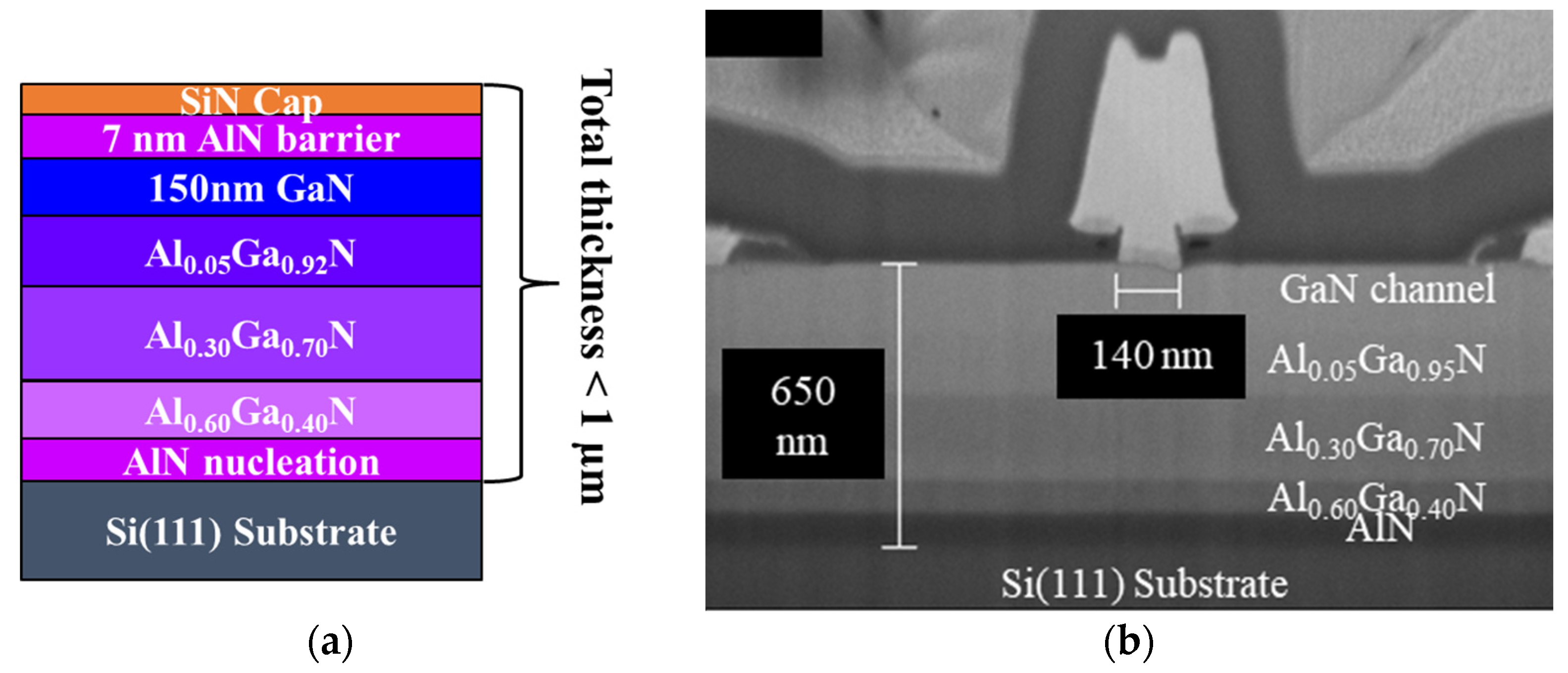
2. Experimental Details

The epitaxial AlN/GaN heterostructure was grown via ammonia–molecular beam epitaxy (NH3-MBE) on 4-inch high-resistivity Si (111) substrates (ρ > 5 KΩ·cm) using a RIBER MBE49 growth reactor. The cross-section and FIB view of the HEMT structures with 140 nm T-gates are shown in Figure 1. It consists of a high-quality lower than 100 nm AlN nucleation layer (NL), followed by a step-graded AlxGa1−xN buffer layers (Al0.05Ga0.92N/Al0.30Ga0.70N/Al0.60Ga0.40N), with a total thickness of 450 nm, a 150 nm thick undoped GaN channel layer, and a 7 nm thick AlN barrier layer. Finally, an in situ SiN layer was used to cap the structure. It can be noticed that the total stack thickness is as low as 650 nm (Figure 1b). The step-graded AlxGa1−xN buffer plays the role of back barrier, increasing the overall buffer bandgap to enhance both the breakdown voltage and the electron confinement under high electric field. The source and drain ohmic contacts were first fabricated. The contacts were directly deposited on top of the AlN barrier. A Ti/Al/Ni/Au metal stack was annealed at 850 °C, yielding contact resistances of 0.4 Ω·mm. Nitrogen implantation was used to isolate the devices. Then, Ni/Au T-gates of 140 nm, 250 nm, and 500 nm gate lengths (LG) were defined by e-beam lithography. Finally, 200 nm PECVD Si3N4 passivation layer was deposited prior to Ti/Au pad deposition. Hall effect measurements at room temperature showed a charge density of 1.7 × 1013 cm−2 with an electron mobility of 745 cm²/V·s. The electron mobility can be significantly improved by further tuning the growth parameters [18].

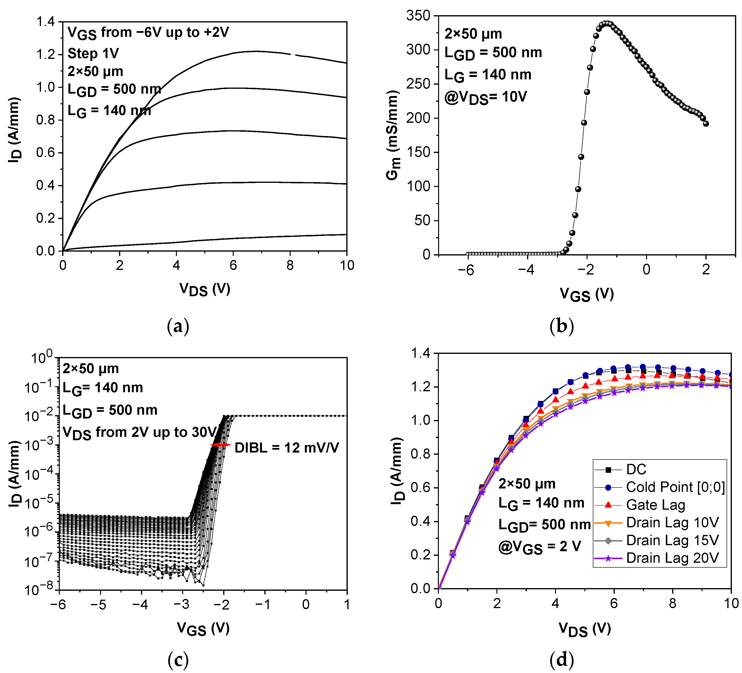
3. DC and RF Characteristics

Thus, 2 × 50 µm transistors with LG = 140 nm and a gate-to-drain distance (LGD) of 500 nm typical output and transfer characteristics are shown in Figure 2. The gate source voltage was swept from −6 V to +2 V with a 1 V step. A maximum drain current density (ID,max) of 1.2 A/mm (Figure 2a) and a transconductance (Gm) of 340 mS/mm were measured (Figure 2b), despite the rather limited electron mobility and access resistances that can still be optimized. Transfer characteristics with a compliance fixed at 150 mA/mm and swept from a drain bias of 2 to 30 V using a 1 V step are displayed in Figure 2c. A drain leakage current lower than 10 µA/mm up to VDS = 30 V (shown in Figure 2c) is uniformly observed. A limited threshold voltage shift is observed as a function of VDS under high electric field, which reflects the proper 2DEG electron confinement confirmed by a low drain-induced barrier lowering (DIBL) of 12 mV/V. The transistors’ three-terminal off-state breakdown voltage was assessed at VGS = −4 V. A hard breakdown voltage between 60 V and 70 V was observed. This translates to a lateral breakdown strength up to 140 V/µm, further proving the quality of the buffer, especially considering the sub-micron total epi-stack thickness.
Figure 2d depicts pulsed ID–VDS characteristics, revealing the electron trapping effects. For various quiescent drain voltages, the open-channel DC-pulsed measurements are shown at VGS = +2 V and at room temperature. A pulse width of 1 μs and a duty cycle of 1% were employed. Thus, 2 × 50 μm transistors with LGD of 500 nm and LG of 140 nm show low-electron trapping effects with about 10% current collapse at VDS = 20 V, despite the low epilayer total thickness. This is attributed to the high nucleation layer quality and subsequent step-graded Al-rich AlGaN layers as well as the absence of doping compensation, such as iron or carbon, which are known to act as acceptors and, thus, generate trapping. Low unintentional carbon and oxygen concentrations within the structure were measured using secondary-ion mass spectrometry (SIMS). The carbon concentration is about 1–5 × 10¹⁵ atoms/cm3, both in the step-graded AlxGa1−xN buffer layers and the GaN channel, while the oxygen concentration is below 1 × 10¹⁷ atoms/cm3 in the buffer layers. The rather low unintentional carbon doping is considered to be satisfactory to avoid buffer-trapping effects [19,20].
The S-parameters were measured for different gate lengths from 250 MHz to 67 GHz with a Rhode and Schwarz ZVA67GHz network analyzer, as shown in Figure 3. The current gain extrinsic cut-off frequency (FT) slightly decreases as a function of VDS and shows a good scaling for short LG (shown in Figure 3a), owing to the reduced short channel effects enabled by the ultrathin barrier. The maximum oscillation frequency (Fmax) increases as a function of VDS (Figure 3b). FT/Fmax of 51/169 GHz are achieved at VDS = 20 V with LGD = 500 nm and LG = 140 nm. The Fmax/FT ratio above 3 for all gate lengths results from the highly favorable aspect ratio: gate length/gate-to-channel distance and the T-gate height higher than 100 nm, ensuring a reduced parasitic gate resistance [21,22].

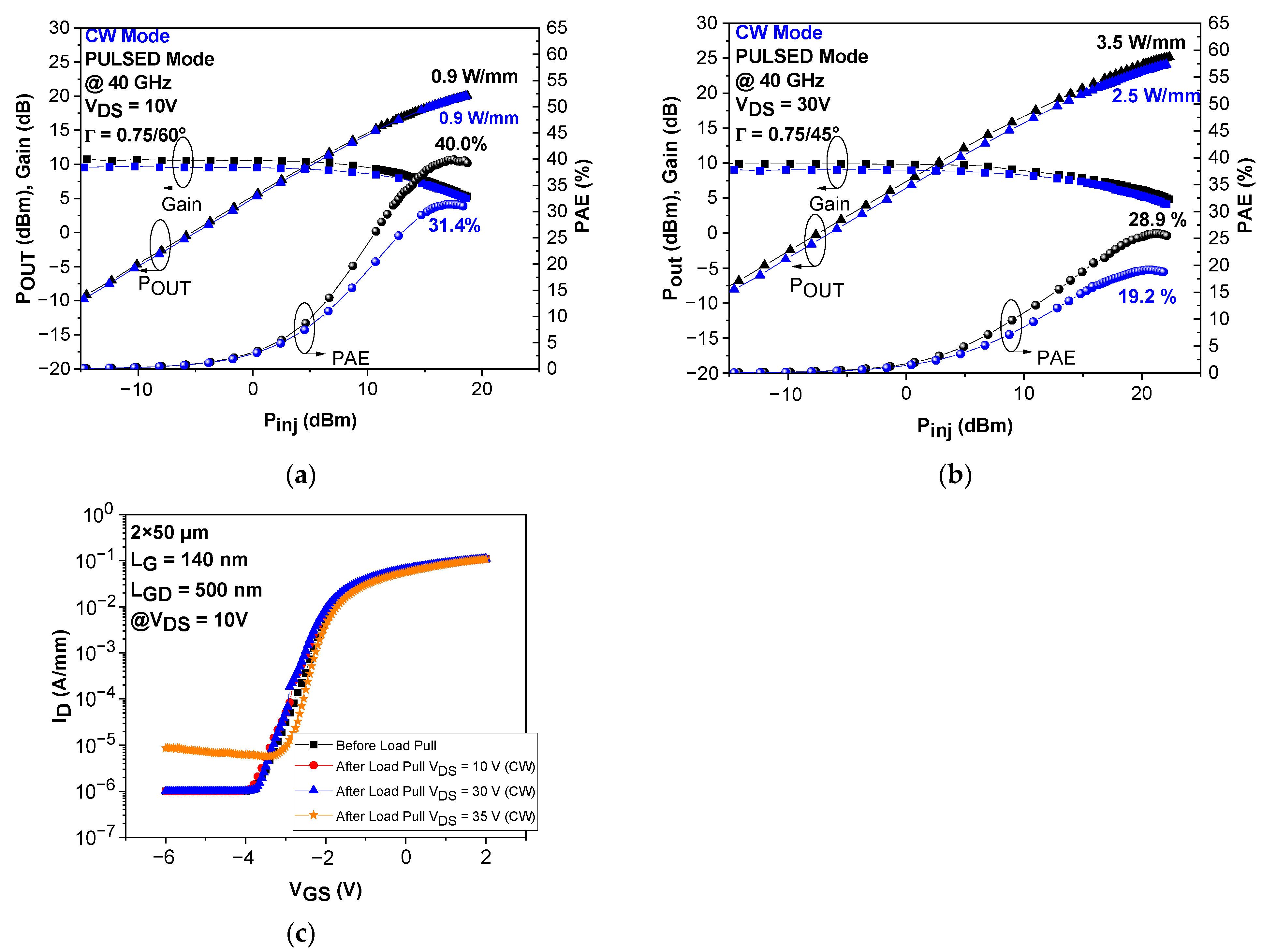
4. Large Signal Characteristics (10 GHz and 40 GHz)

Large signal characterizations were carried out at 10 GHz and 40 GHz on a nonlinear vector network analyzer system (Keysight Network Analyser: PNA-X, N5245A-NVNA) capable of on-wafer large signal device characterization up to the Q-band in continuous-wave (CW) and pulsed mode. Further details about the power bench can be found in Ref. [23]. Figure 4a,b show typical CW and pulsed mode power performances at 10 GHz in deep class AB of 2 × 50 µm transistors with LGD = 500 nm and LG = 140 nm at VDS = 10 V and 30 V, respectively. A 1.1 W/mm saturated output power density (POUT) with a power-added efficiency (PAE) of 53.6% and 47.2% at VDS = 10 V is measured in pulsed and CW mode, respectively. As expected, at VDS = 30 V, the POUT increases substantially well above 3 W/mm with a PAE > 42%. Figure 5a,b show CW and pulsed power performances at 40 GHz of similar 2 × 50 µm transistors with LG = 140 nm at VDS = 10 V and 30 V, respectively. A saturated POUT close to 1 W/mm associated to a PAE of 40.0% and 31.4% at VDS = 10 V is measured in pulsed and CW mode, respectively. At VDS = 30 V, a POUT of 3.5 W/mm and 2.5 W/mm with a PAE of 28.9% and 19.2% are observed in pulsed and CW mode, respectively. Moreover, it can be pointed out that following several tenths of CW Load-Pull sweeps under high-gain compression (up to 10 dB), we did not observe any major degradation of the devices up to VDS = 30 V (see Figure 5c). Degradation reflected by an increase in the off-state leakage current is observed at a bias VDS as high as 35 V (see Figure 5c), while typical safe operating drain bias for mm wave GaN-on-silicon HEMTs is well below 20 V. This indicates an excellent robustness of this heterostructure, handling an extreme electric field and, thus, enabling high-voltage operation without degradation while using a sub-150 nm gate length. The promising device reliability results from the excellent electron confinement and low trapping effects despite the absence of any thermal management. Indeed, unlike semi-insulating SiC substrates that are favorable for high-power operation, silicon has a much lower dissipation, which results in significantly higher junction temperature in GaN-on-silicon HEMTs.
Figure 6 depicts typical pulsed PAE and POUT of 2 × 50 µm AlN/GaN on silicon transistors with LGD = 500 nm and LG = 140 nm as a function of VDS at 40 GHz. The PAE decreases with the VDS increase but remains about 30% under 3.5 W/mm at VDS = 30 V, which sets a new performance benchmark at this frequency band for GaN-on-Si HEMTs (Figure 6b). As shown in Figure 6c, it can be pointed out that this represents the first high-performance mm wave transistors using a sub-micron-thick GaN-on-silicon heterostructure. The drop in the PAE/POUT between pulsed and CW measurements is mainly attributed to the low thermal dissipation of the Si substrate, as seen from the increasing CW/pulsed POUT gap that is more pronounced under higher output power. Therefore, further optimization of the structure to enhance the electron mobility and, thus, the power gain, combined with well-known techniques, such as substrate thinning/or vias, with subsequent related heat sink based on copper will certainly boost these reported GaN-on-Si mm wave device performances [24].

5. Conclusions

We developed a sub-micron-thick AlN/GaN heterostructure grown via NH3-MBE on a silicon substrate, enabling the combination of low-electron trapping effects, extreme robustness under a high electric field, and high mm wave power gain. This, in turn, allows for unprecedented class AB bias operation (up to VDS = 30 V) for 140 nm gate-length GaN-on-Si HEMTs. Consequently, the proposed AlN/GaN-on-silicon HEMT structure delivers high-output power density together with state-of-the-art PAE of 40%/29% at VDS = 10 V/30 V at 40 GHz, respectively. This achievement is attributed to the optimization of material, epi-design, and processing quality, enabling a high-electron confinement together with reduced short channel effects under a high electric field. The results show the potential of MBE to grow ultrathin cost-effective AlN/GaN-on-Si HEMTs for mm wave applications.

Author Contributions

Material growth, S.R., S.T. and F.S.; device processing, E.C. and F.M.; device characterization, E.C., K.H. and F.M.; validation, E.C., S.R., S.T., K.H., F.S. and F.M.; writing—review and editing, E.C., S.R., S.T., K.H., F.S. and F.M.; funding acquisition, F.S. and F.M. All authors have read and agreed to the published version of the manuscript.

Funding

This research was funded by the French National grant GaNeXT ANR-11-LABX-0014, and by a BPI France aid for innovation.

Data Availability Statement

The dataset is not applicable.

Acknowledgments

This work was supported by the French RENATECH network, the French National grant GaNeXT ANR-11-LABX-0014, and by a BPI France aid for innovation. The authors would also like to thank Riber for his amazing technical support.

Conflicts of Interest

The authors declare no conflict of interest. The funders had no role in the design of the study; in the collection, analyses, or interpretation of data; in the writing of the manuscript; or in the decision to publish the results.

References

  1. Mishra, U.K.; Parikh, P.; Wu, Y.F. AlGaN/GaN HEMTs—An overview of device operation and applications. Proc. IEEE 2002, 90, 1022–1031. [Google Scholar] [CrossRef]
  2. Moon, J.S.; Wong, D.; Hu, M.; Hashimoto, P.; Antcliffe, M.; McGuire, C.; Micovic, M.; Willadson, P. 55% PAE and high power Ka-band GaN HEMTs with linearized transconductance via n+ GaN source contact ledge. IEEE Electron Device Lett. 2008, 29, 834–837. [Google Scholar] [CrossRef]
  3. Jazaeri, F.; Sallese, J.M. Charge-based EPFL HEMT model. IEEE Trans. Electron. Devices 2019, 66, 1218–1229. [Google Scholar] [CrossRef]
  4. Liu, W.; Romanczyk, B.; Guidry, M.; Hatui, N.; Wurm, C.; Li, W.; Shrestha, P.; Zheng, X.; Keller, S.; Mishra, U.K. 6.2 W/Mm and Record 33.8% PAE at 94 GHz from N-Polar GaN Deep Recess MIS-HEMTs with ALD Ru Gates. IEEE Microw. Wirel. Compon. Lett. 2021, 31, 748–751. [Google Scholar] [CrossRef]
  5. Moon, J.S.; Grabar, R.; Wong, J.; Antcliffe, M.; Chen, P.; Arkun, E.; Khalaf, I.; Corrion, A.; Chappell, J.; Venkatesan, N.; et al. High-speed graded-channel AlGaN/GaN HEMTs with power added efficiency >70% at 30 GHz. Electron. Lett. 2020, 56, 678–680. [Google Scholar] [CrossRef]
  6. Makiyama, K.; Ozaki, S.; Ohki, T.; Okamoto, N.; Minoura, Y.; Niida, Y.; Kamada, Y.; Joshin, K.; Watanabe, K.; Miyamoto, Y. Collapse-free high power InAlGaN/GaN-HEMT with 3 W/mm at 96 GHz. In Proceedings of the 2015 Technical Digest—International Electron Devices Meeting (IEDM), Washington, DC, USA, 7–9 December 2015. [Google Scholar] [CrossRef]
  7. Moench, S.; Müller, S.; Reiner, R.; Waltereit, P.; Czap, H.; Basler, M.; Hückelheim, J.; Kirste, L.; Kallfass, I.; Quay, R.; et al. Monolithic Integrated AlGaN/GaN Power Converter Topologies on High-Voltage AlN/GaN Superlattice Buffer. Phys. Status Solidi (A) Appl. Mater. Sci. 2021, 218, 2000404. [Google Scholar] [CrossRef]
  8. Chang, J.; Afroz, S.; Nagamatsu, K.; Frey, K.; Saluru, S.; Merkel, J.; Taylor, S.; Stewart, E.; Gupta, S.; Howell, R. The Super-Lattice Castellated Field-Effect RF Amplifier. IEEE Electron Device Lett. 2019, 40, 1048–1051. [Google Scholar] [CrossRef]
  9. Micovic, M.; Brown, D.F.; Regan, D.; Wong, J.; Tang, Y.; Herrault, F.; Santos, D.; Burnham, S.D.; Tai, J.; Prophet, E.; et al. High Frequency GaN HEMTs for RF MMIC Applications. In Proceedings of the 2016 IEEE International Electron Devices Meeting (IEDM), San Francisco, CA, USA, 3–7 December 2016. [Google Scholar] [CrossRef]
  10. Chen, D.Y.; Malmros, A.; Thorsell, M.; Hjelmgren, H.; Kordina, O.; Chen, J.T.; Rorsman, N. Microwave Performance of “Buffer-Free” GaN-on-SiC High Electron Mobility Transistors. IEEE Electron Device Lett. 2020, 41, 828–831. [Google Scholar] [CrossRef]
  11. Chen, D.Y.; Wen, K.H.; Thorsell, M.; Lorenzini, M.; Hjelmgren, H.; Chen, J.T.; Rorsman, N. Impact of the Channel Thickness on Electron Confinement in MOCVD-Grown High Breakdown Buffer-Free AlGaN/GaN Heterostructures. Phys. Status Solidi (A) Appl. Mater. Sci. 2022, 2022, 2200496. [Google Scholar] [CrossRef]
  12. Jessen, G.H.; Fitch, R.C.; Gillespie, J.K.; Via, G.; Crespo, A.; Langley, D.; Denninghoff, D.J.; Trejo, M.; Heller, E.R.; Algan, A. Short-Channel Effect Limitations on High-Frequency Operation of AlGaN/GaN HEMTs for T-Gate Devices. IEEE Trans. Electron. Devices 2007, 54, 2589–2597. [Google Scholar] [CrossRef]
  13. Schwantuschke, D.; Godejohann, B.J.; Brückner, P.; Tessmann, A.; Quay, R. mm-Wave Operation of AlN/GaN-Devices and MMICs at V- & W-band. In Proceedings of the IEEE 22nd International Microwave and Radar Conference (MIKON), Poznan, Poland, 14–17 May 2018. [Google Scholar] [CrossRef]
  14. Gao, Z.H.; Meneghini, M.; Harrouche, K.; Kabouche, R.; Chiocchetta, F.; Okada, E.; Rampazzo, F.; De Santi, C.; Medjdoub, F.; Meneghesso, G.; et al. Short term reliability and robustness of ultra-thin barrier, 110 nm-gate AlN/GaN HEMTs. Microelectron. Reliab. 2021, 123, 1–6. [Google Scholar] [CrossRef]
  15. Harrouche, K.; Kabouche, R.; Okada, E.; Medjdoub, F. High Power AlN/GaN HEMTs with record power-added-efficiency >70% at 40 GHz. In Proceedings of the 2020 IEEE/MTT-S International Microwave Symposium (IMS), Los Angeles, CA, USA, 4–6 August 2020. [Google Scholar] [CrossRef]
  16. Godejohann, B.J.; Ture, E.; Müller, S.; Prescher, M.; Kirste, L.; Aidam, R.; Polyakov, V.; Brückner, P.; Breuer, S.; Köhler, K.; et al. AlN/GaN HEMTs grown by MBE and MOCVD: Impact of Al distribution. Phys. Status Solidi B Basic Res. 2017, 254, 3–7. [Google Scholar] [CrossRef]
  17. Medjdoub, F.; Kabouche, R.; Linge, A.; Grimbert, B.; Zegaoui, M.; Gamarra, P.; Lacam, C.; Tordjman, M.; Di Forte-Poisson, M.A. High electron mobility in high-polarization sub-10 nm barrier thickness InAlGaN/GaN heterostructure. Appl. Phys. Express 2015, 8, 5–9. [Google Scholar] [CrossRef]
  18. Yang, L.; Wang, X.; Wang, T.; Wang, J.; Zhang, W.; Quach, P.; Wang, P.; Liu, F.; Li, D.; Chen, L.; et al. Three Subband Occupation of the Two-Dimensional Electron Gas in Ultrathin Barrier AlN/GaN Heterostructures. Adv. Funct. Mater. 2020, 30, 2004450. [Google Scholar] [CrossRef]
  19. Harrouche, K.; Venkatachalam, S.; Grandpierron, F.; Okada, E.; Medjdoub, F. Impact of undoped channel thickness and carbon concentration on AlN/GaN-on-SiC HEMT performances. Appl. Phys. Express 2022, 15, 116504. [Google Scholar] [CrossRef]
  20. Pradhan, M.; Alomari, M.; Moser, M.; Di, F.; Hahn, H.; Heuken, M.; Burghartz, J.N. Physical Modeling of Charge Trapping Effects in GaN/Si Devices and Incorporation in the ASM-HEMT Model. IEEE J. Electron. Devices Soc. 2021, 9, 748–755. [Google Scholar] [CrossRef]
  21. Shinohara, K.; Regan, D.C.; Tang, Y.; Corrion, A.L.; Brown, D.F.; Wong, J.C.; Robinson, J.F.; Fung, H.H.; Schmitz, A.; Oh, T.C.; et al. Scaling of GaN HEMTs and Schottky Diodes for Submillimeter-Wave MMIC Applications. IEEE Trans. Electron. Devices 2013, 60, 2982–2996. [Google Scholar] [CrossRef]
  22. Allaei, M.; Shalchian, M.; Jazaeri, F. Modeling of Short-Channel Effects in GaN HEMTs. IEEE Trans. Electron. Devices 2020, 67, 3088–3094. [Google Scholar] [CrossRef]
  23. Kabouche, R.; Okada, E.; Dogmus, E.; Linge, A.; Zegaoui, M.; Medjdoub, F. Power Measurement Setup for On-Wafer Large Signal Characterization Up to Q-Band. IEEE Microw. Wirel. Compon. Lett. 2017, 27, 419–421. [Google Scholar] [CrossRef]
  24. Mohanty, S.K.; Chen, Y.Y.; Yeh, P.H.; Horng, R.H. Thermal Management of GaN-on-Si High Electron Mobility Transistor by Copper Filled Micro-Trench Structure. Sci. Rep. 2019, 9, 19691. [Google Scholar] [CrossRef] [Green Version]
  25. Rennesson, S.; Lecourt, F.; Defrance, N.; Chmielowska, M.; Chenot, S.; Lesecq, M.; Hoel, V.; Okada, E.; Cordier, Y.; De Jaeger, J.C. Optimization of Al0.29Ga0.71N/GaN high electron mobility heterostructures for high-power/frequency performances. IEEE Trans. Electron. Devices 2013, 60, 3105–3111. [Google Scholar] [CrossRef]
  26. Altuntas, P.; Lecourt, F.; Cutivet, A.; Defrance, N.; Okada, E.; Lesecq, M.; Rennesson, S.; Agboton, A.; Cordier, Y.; Hoel, V.; et al. Power Performance at 40 GHz of AlGaN/GaN High-Electron Mobility Transistors Grown by Molecular Beam Epitaxy on Si(111) Substrate. IEEE Electron Device Lett. 2015, 36, 303–305. [Google Scholar] [CrossRef]
  27. Soltani, A.; Gerbedoen, J.C.; Cordier, Y.; Ducatteau, D.; Rousseau, M.; Chmielowska, M.; Ramdani, M.; De Jaeger, J.C. Power performance of AlGaN/GaN high-electron-mobility transistors on (110) silicon substrate at 40 GHz. IEEE Electron Device Lett. 2013, 34, 490–492. [Google Scholar] [CrossRef]
  28. Medjdoub, F.; Zegaoui, M.; Grimbert, B.; Ducatteau, D.; Rolland, N.; Rolland, P.A. First demonstration of high-power GaN-on-silicon transistors at 40 GHz. IEEE Electron Device Lett. 2012, 33, 1168–1170. [Google Scholar] [CrossRef]
  29. Marti, D.; Tirelli, S.; Alt, A.R.; Roberts, J.; Bolognesi, C.R. 150-GHz cutoff frequencies and 2-W/mm output power at 40 GHz in a millimeter-wave AlGaN/GaN HEMT technology on silicon. IEEE Electron Device Lett. 2012, 33, 1372–1374. [Google Scholar] [CrossRef]
Figure 1. (a) Schematic cross-section and (b) FIB view of the ultrathin AlN/GaN HEMTs grown on Si(111) substrate by MBE and using a step-graded AlxGa1−xN buffer layers.
Electronics 12 02974 g001
Figure 2. (a) Output characteristics, (b) extrinsic transconductance, (c) transfer characteristics up to VDS = 30 V, and (d) open channel pulsed ID-VDS output characteristics of 2 × 50 µm ultrathin AlN/GaN-on-Si HEMTs with LGD = 500 nm and LG = 140 nm.
Electronics 12 02974 g002
Figure 3. (a) Current gain extrinsic cut-off frequency and (b) maximum oscillation frequency of 2 × 50 µm ultrathin AlN/GaN HEMTs with LGD = 500 nm for various gate lengths.
Electronics 12 02974 g003
Figure 4. CW and pulsed large signal performances at 10 GHz of 2 × 50 µm ultrathin AlN/GaN HEMTs with LGD = 500 nm and LG = 140 nm at (a) VDS = 10 V and (b) VDS= 30 V.
Electronics 12 02974 g004
Figure 5. Typical CW and pulsed large signal performances at 40 GHz of 2 × 50 µm ultrathin AlN/GaN HEMTs with LGD = 500 nm and LG = 140 nm at (a) VDS = 10 V and (b) VDS= 30 V. (c) Transfer characteristics after more than 40 CW Load-Pull sweeps in deep class AB under high compression up to VDS = 35 V.
Electronics 12 02974 g005
Figure 6. (a) Pulsed PAE and POUT as a function of VDS at 40 GHz with LGD = 500 nm and LG = 140 nm for 2 × 50 µm ultrathin AlN/GaN HEMTs. Benchmark of (b) power performances and (c) PAE as a function of total stack thickness at 40 GHz for GaN-on-Si HEMTs [25,26,27,28,29].
Electronics 12 02974 g006
Disclaimer/Publisher’s Note: The statements, opinions and data contained in all publications are solely those of the individual author(s) and contributor(s) and not of MDPI and/or the editor(s). MDPI and/or the editor(s) disclaim responsibility for any injury to people or property resulting from any ideas, methods, instructions or products referred to in the content.

