Article

Comparative Performance Evaluation of Conventional and Folded Detector Structures: Application to Perovskite X-ray Detectors

Department of Electrical and Computer Engineering, Concordia University, 1455 Boul. de Maisonneuve Ouest, Montréal, QC H3G 1M8, Canada
*
Author to whom correspondence should be addressed.
Electronics 2023, 12(13), 2976; https://doi.org/10.3390/electronics12132976
Submission received: 30 May 2023 / Revised: 2 July 2023 / Accepted: 3 July 2023 / Published: 6 July 2023
(This article belongs to the Special Issue Emerging Optoelectronics Devices: Materials, Designs and Applications)

Abstract

:
The imaging performance of a semiconductor radiation imaging detector critically depends on its photoconductor layer thickness. The conventional detector structure (i.e., a photoconductor layer is sandwiched between two parallel electrodes) needs a strict design criterion on photoconductor thickness as compared to folded detector structure for optimizing the detective quantum efficiency (DQE), which is the most important imaging performance. In this paper, the DQE performance of both folded and conventional detector structures is analyzed by incorporating the quantum noise due to random charge carrier trapping in the photoconductor layer in the cascaded linear system model. An analytical expression for the variance of incomplete charge collection in folded structure is also developed. The optimum values of photoconductor layer thickness and spacing between electrodes for maximizing the DQE under various combinations of exposure, electronic noise and charge carrier transport parameters are investigated. The folded structure provides a design flexibility for achieving DQE higher than 0.7 by adjusting the distance between electrodes without compromising the quantum efficiency while the maximum possible DQE in conventional structure can be even below 0.3 for certain values of material and detector parameters.

1. Introduction

X-ray photoconductor-based flat-panel X-ray imagers (FPXIs) produce superior X-ray image as compared to scintillator-based detectors and are the commercially available digital X-ray detectors for mammography [1,2]. These detectors are, at present, under scrutiny for use in general radiography, fluoroscopy, tomosynthesis and portal imaging [3,4]. Amorphous selenium (a-Se) is the most successful photoconductor for photoconductor-based X-ray detectors because it can be conveniently deposited over large area at low-temperature and a-Se based detectors show low dark current and good charge-transport properties. There is one important drawback of a-Se, which is its lower intrinsic X-ray sensitivity (i.e., its large ionization energy, Wi, which is the minimum radiation energy required to create a single electron-hole pair, EHP) as compared to other X-ray photoconductors such as polycrystalline HgI2 or CdZnTe [5]. For example, the value of Wi in a-Se is about 45 eV at the typical operating the electric field of 10 V/μm whereas the value of Wi is 5–6 eV for other X-ray photoconductors. Lower Wi provides more EHP generation and improves the signal strength (i.e., higher X-ray sensitivity) and signal to noise ratio. However, the basic underlying problem with most of these polycrystalline detectors is that they exhibit either an unacceptably large dark current (a current that flows in the detector in absence of irradiation) or they possesses significantly low charge collection efficiency [5,6]. There has been an active search going on to find efficient alternate X-ray photoconductors [5].
The use of Hybrid Organic−Inorganic Perovskites (HOIPs) in large area X-ray imaging detectors was first realized in 2015 when Yakunin et al. [7] first demonstrated a prototype X-ray detector using a thick layer (~100 μm) of polycrystalline methylammonium lead iodide (poly-MAPbI3 where MA is CH3NH3) perovskite photoconductor. This initial prototype detector showed a very high dark current. Later, Kim et al. [8] proposed a multilayer structure using blocking layers to poly-MAPbI3 detectors to reduce the dark current. Their structure showed reasonably low dark current, good X-ray sensitivity but very poor resolution in terms of the modulation transfer function (MTF). Deumel et al. [9] reported slightly better resolution in their 230 μm thick MAPbI3 detector. Recently, Y. Li [10] et al. demonstrated much lower dark current in their perovskite detector structures.
The photoconductor layer thickness plays a very important role in conventional detector structure (i.e., a photoconductor layer is sandwiched between two electrodes where charges are collected in corresponding pixels) on imaging performances [5,8]. A relatively thicker layer is required for better sensitivity. However, the thicker layer contributes to more noise and signal spreading as carriers must travel a longer distance to reach the electrodes, and thus adversely affects image resolution and detective quantum efficiency (DQE) [11,12]. Recently, Mescher et al. [13] proposed a folded structure where charge carriers travel perpendicular to the direction of incident X-rays. Note that the charge carrier transport mechanism in folded structure is similar to a co-planar detector structure [14]. In folded structure the X-ray quantum efficiency can be improved using a thicker layer without affecting the charge collection by keeping the charge collecting electrodes at a reasonable distance. They theoretically analyzed the DQE using an oversimplified analytical model. In their model, they didn’t consider the quantum noise due to random nature of charge carrier trapping, which is a very important factor for accurate modeling of the detective quantum efficiency [15].
In this paper, we have analyzed the detective quantum efficiency of both folded and conventional detector structures by incorporating the quantum noise due to random charge carrier trapping. We have developed an analytical expression for the variance of charge collection in folded structure. The folded structure provides more design flexibility for optimum DQE. The optimum values of photoconductor layer thickness and spacing between electrodes for maximizing the DQE under various material parameters and detector operating conditions are investigated.

2. Theory

The DQE measures the relative change of signal to noise ratio from its input to its output through various stages of an imaging system. The X-ray image can be degraded by various sources of stochastic and deterministic signal fluctuations which arise along the imaging chain. The DQE is expressed quantitatively as
DQE = SNR out 2 SNR in 2 ,
where SNRin and SNRout are the signal to noise ratio at the input and output stages of an image detector, respectively.

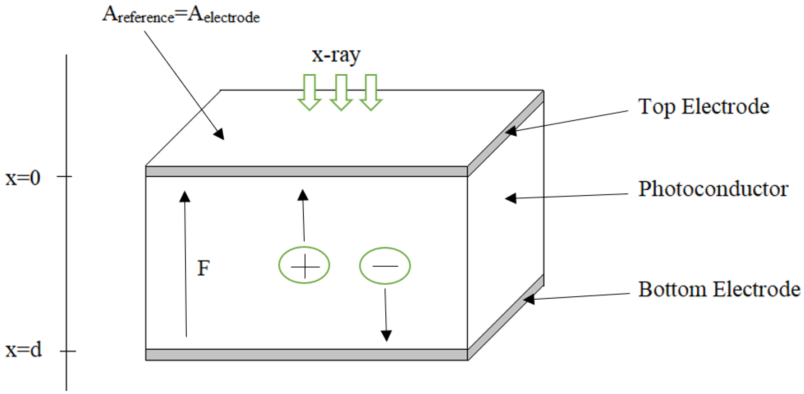
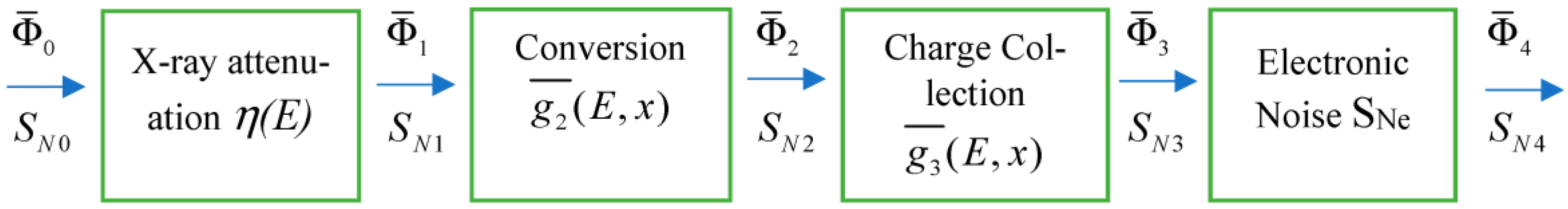
2.1. Conventional Planner Structure

The conventional detector structure, a photoconductor layer has been sandwiched between two large area parallel plate electrodes and a bias voltage is applied between the two electrodes to establish an electric field F, is shown in Figure 1.
The DQE performance of many imaging systems is usually analyzed by developing a cascaded linear system model in which the imaging system is described as cascades of simple and independent elementary stages. The cascaded linear system model for calculating DQE (without considering signal spreading) of a detector that is shown in Figure 2 consists of four stages: (1) X-ray attenuation, (2) the creation of EHPs (conversion gain), (3) charge collection process, and (4) the addition of electronic noise. The flow chart shown in Figure 2 illustrates the signals and noise power after every stage. Since the spatial spreading of signal and noise are not considered, the DQE analysis in this work represents the zero spatial frequency detective quantum efficiency DQE.
Each of the first three stages is defined as a stochastic gain stage. For the stochastic gain stage i the output mean signal quanta and noise power spectrum (NPS) per unit area arising from incident X-ray photon interactions at depth x from the radiation-receiving electrode are, respectively [16],
Φ ¯ i ( E , x ) = g ¯ i ( E , x ) Φ ¯ i 1 ( E , x )
S N i ( E , x ) = g ¯ i 2 ( E , x ) S N ( i 1 ) ( E , x ) + σ g i 2 ( E , x ) Φ ¯ i 1 ( E , x )
where E is the incident X-ray photon energy, Φ ¯ i 1 ( E , x ) and S N ( i 1 ) ( E , x ) are the mean number of quanta and the NPS incident on stage i, respectively, and g ¯ i ( E , x ) and σgi2(E, x) are the mean gain and variance of the gain of the ith stage. The first term in Equation (3) represents the amplification of the quantum noise and the second term represents an additional noise due to the random fluctuation of the amplification gain of the ith stage. Following the flow chart in Figure 2, the mean gain and the variance of gain of each stage are determined as follows.
The gain of the X-ray attenuation stage is the quantum efficiency η of the detector, which is given by,
η ( E ) = 1 e α d ,
where E is the incident X-ray photon energy, α(E) and d are the linear attenuation coefficient and the distance between two electrodes (which is the same as the photoconductor layer thickness), respectively. An incident X-ray photon on this selection stage either interacts with the detector, probability η, or does not, probability (1 − η). Therefore, this is a binary selection process [17]. According to the binomial theorem, the variance of η,
σ g 1 2 = η ( 1 η ) .
The mean conversion gain g ¯ 2 ( E , x ) of the second stage represents the mean number of EHPs generated after the absorption of an X-ray photon interaction at x is,
g ¯ 2 ( E , x ) = E a b ( E , x ) W i ,
where Eab(E, x) is the average absorbed energy per X-ray photon of energy E. For a relatively thinner detector, the reabsorption probability of the secondary photons is small and thus Eab(E) ≈ (αen/α)E, where αen is the energy absorption coefficient of the photoconductor. On the other hand, the secondary photons are mostly reabsorbed in a thicker detector (i.e., in detectors with high η) and thus, EabE.
There is a fluctuation in conversion gain due to the stochastic fluctuation of the number of EHP generation per X-ray photon. We assume that the mean number of free EHPs released per X-ray photon obeys a Poisson process, i.e., σ g 2 2 ( E ) g ¯ 2 ( E ) [16,18].
The electric field remains relatively uniform across the photoconductor layer and bimolecular recombination is negligible in small signals, which is quite appropriate for medical diagnostic applications [19]. The diffusion of carriers is negligible compared with their drift counterpart because of relatively high applied fields across the photoconductor. The general transport behavior in many photoconductors can be described in terms of a constant drift mobility μ and a single carrier lifetime τ for each type of carriers (holes and electrons) [16]. With these assumptions above, the average charge collection efficiency, g ¯ 3 ( x ) , at the electrodes from EHP generation at coordinate x can be written as [20],
g ¯ 3 ( x ) = x t ( 1 e x d x t ) + x b ( 1 e d x d x b )
where xt = μtτtF/d, xb = μbτbF/d. The subscript t and b refer to carrier types drifting to the top and bottom electrodes respectively; the top electrode receives the X-ray radiation. The variance of charge collection due to random trapping for an EHP generation at x is given by [15],
σ g 3 2 ( x ) = x t 2 + x b 2 x t 2 e 2 x d x t x b 2 e 2 ( d x ) d x b 2 x t x d e x d x t 2 x b ( 1 x d ) e d x d x b
During image readout, the image signal passes through TFT/CMOS switch and charge amplifiers and thus the equivalent electronic noise power SNe associated with these electronic components is added to the total noise power [12].
The input noise in the number of X-ray quanta incident on the detector is usually considered to follow a Poisson process and thus the input NPS is S N 0 = Φ ¯ 0 , where Φ ¯ 0 is the mean number of incident X-ray photons per unit area. Thus, the square of signal to noise ratio at the input,
SNR in 2 = Φ ¯ 0 .
The X-rays are attenuated exponentially across the photoconductor thickness. Therefore, the probability density function for an X-ray photon, that is attenuated within a detector, to interact at a distance x from the top electrode is,
P x ( x ) = α η e α x   ; 0 x d
Applying Equations (2) and (3) successively, the expected total signal at the output of the third stage is,
Φ ¯ 3 = η Φ ¯ 0 g ¯ 2 0 d g ¯ 3 ( x ) p x ( x ) d x = η Φ ¯ 0 g ¯ 2 η ¯ c c
where the average charge collection efficiency,
η ¯ c c = x t { 1 1 e 1 Δ 1 x t ( 1 e 1 Δ ) ( 1 + Δ x t ) } + x b { 1 + e 1 x b e 1 Δ ( 1 e 1 Δ ) ( Δ x b 1 ) }
Similarly, the NPS at the output of third stage is,
S N 3 = Φ ¯ 0 η g ¯ 2 0 d { g ¯ 3 2 ( x ) [ 1 + g ¯ 2 ] + σ g 3 2 ( x ) } P x ( x ) d x ,
S N 3 = η Φ ¯ 0 g ¯ 2 ( g ¯ 2 + 1 ) [ x t 2 ( 1 + x t A ) + 2 x t x b B + x b 2 ( 1 + x b C ) ] + η Φ ¯ 0 g ¯ 2 [ x t 2 ( 1 + D ) + x b 2 ( 1 + E ) + x t 3 F + x b 3 G ]
where,
A = 2 η a ( e 1 x t 1 Δ 1 ) η b ( e 2 x t 1 Δ 1 ) ,
B = 1 + x t η a ( e 1 x t 1 Δ 1 ) x b η c ( e 1 Δ e 1 x b ) + x t x b η e ( e 1 x t 1 Δ e 1 x b ) ,
C = η d ( e 1 Δ e 2 x b ) 2 η c ( e 1 Δ e 1 x b ) ,
D = 2 η a e 1 x t 1 Δ ,
E = 2 η c e 1 x b ,
F = η b ( e 2 x t 1 Δ 1 ) 2 η f ( 1 e 1 x t 1 Δ ) ,
G = η d ( e 1 Δ e 2 x b ) 2 η g ( e 1 Δ e 1 x b ) ,
η a = 1 η Δ ( 1 + x t Δ ) ,   η b = 1 η Δ ( 2 + x t Δ ) ,
η c = 1 η Δ ( 1 x b Δ ) ,   η d = 1 η Δ ( 2 x b Δ ) ,
η e = 1 η Δ ( x t x b x t x b Δ ) ,   η f = 1 η Δ ( 1 + x t Δ ) 2 ,
and η g = 1 η Δ ( 1 x b Δ ) 2 .
Using Equation (1), the DQE at the output of the detector is
DQE = Φ ¯ 3 2 Φ ¯ 0 ( S N 3 + S N e )

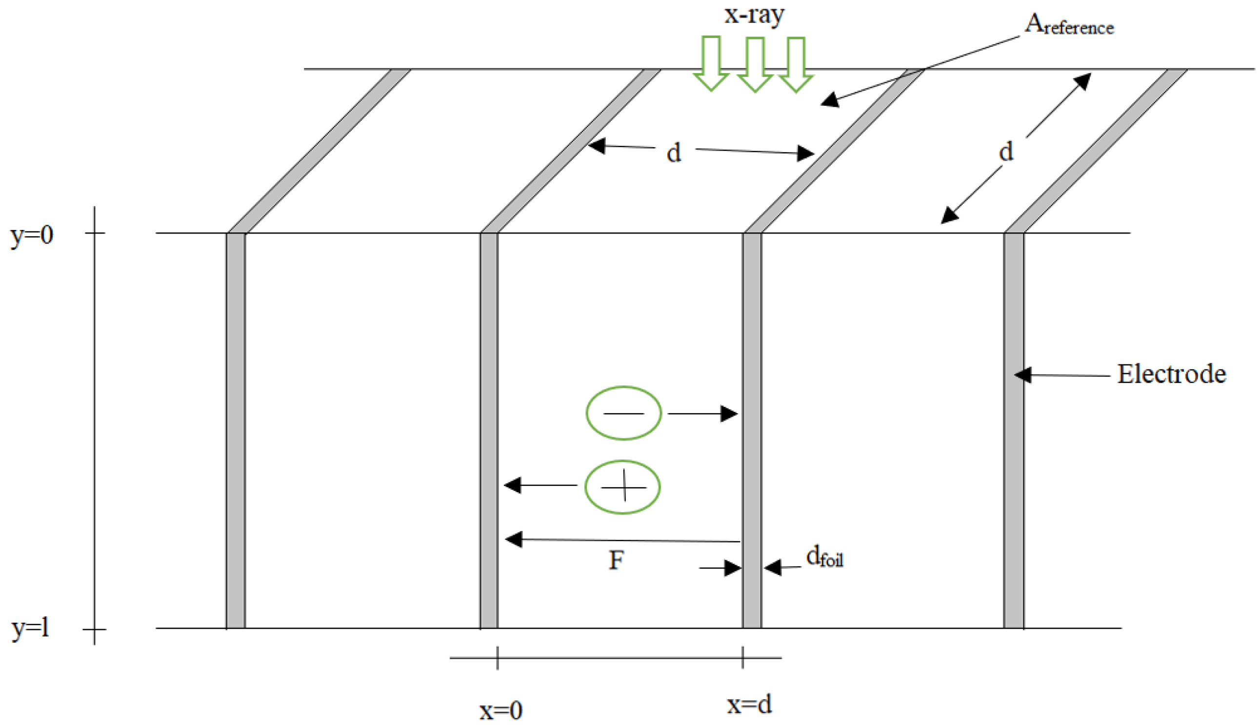
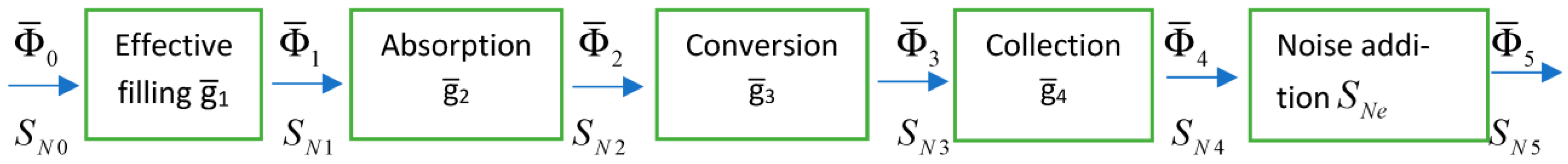
2.2. Folded Structure

The schematic diagram of a folded structure is shown in Figure 3, where the X-rays are attenuated along the y-axis and the X-ray generated charge carriers drift along the x-axis. The detail description of the folded structure was given in Ref. [13]. The quantum efficiency for the folded structure can be expressed as
η ( E ) = 1 e α ( E ) l
where l is photoconductor thickness.
The cascaded linear system model for calculating DQE of a folded structure has an additional stochastic gain stage, named as “effective filling” as shown in Figure 4.
The X-ray absorption in the electrode volume does not contribute to the EHP generation and this loss can be determined by the effective fill factor [13],
g ¯ 1 = d d + d f o i l
where the width of the electrode is dfoil. The gain of this stage is g1. Assuming a binomial selection process [13], the variance of gain σ g 1 2 = g ¯ 1 ( 1 g ¯ 1 ) .
Equations (6) and (7) are applicable for calculating the average charge collection g ¯ 4 ( x ) and the variance of charge collection σ 4 2 ( x ) at the electrodes from EHP generation at coordinate x. However, the probability density function per unit area for an X-ray photon to interact at a distance y from the top electrode is,
p x y ( y ) = α η d e α y   ; 0 y l
The total output signal after fourth stage,
Φ ¯ 4 = η Φ ¯ 0 g ¯ 1 g ¯ 3 0 d 0 l g ¯ 4 ( x ) p x y ( y ) d y d x = η Φ ¯ 0 g ¯ 1 g ¯ 3 η ¯ c c
where,
η ¯ c c = ( x t + x b ) x t 2 ( 1 e 1 x t ) x b 2 ( 1 e 1 x b )
The NPS at the output of fourth stage is,
S N 4 = Φ ¯ 0 η g ¯ 1 g ¯ 3 0 d 0 l { g ¯ 4 2 ( x ) [ 1 + g ¯ 3 ] + σ g 4 2 ( x ) } p x y ( y ) d y d x
S N 4 = g ¯ 3 g ¯ 1 Φ ¯ 0 η ( 1 + g ¯ 3 ) [ x t 2 { 1 + 2 x t ( e 1 x t 1 ) x t 2 ( e 2 x t 1 ) } + 2 x t x b { 1 + x t ( e 1 x t 1 ) x b ( 1 e 1 x b ) + x t x b x t x b ( e 1 x t e 1 x b ) } + x b 2 { 1 2 x b ( 1 e 1 x b ) + x b 2 ( 1 e 2 x b ) } ] + g ¯ 3 g ¯ 1 η Φ ¯ 0 [ x t 2 { 1 + x t 2 ( e 2 x t 1 ) + 2 e 1 x t + 2 x t ( e 1 x t 1 ) } + x b 2 { 1 + x b 2 ( e 2 x b 1 ) + 2 e 1 x b + 2 x b ( e 1 x b 1 ) } ]
The DQE at the output (after fifth stage),
DQE = Φ ¯ 4 2 Φ ¯ 0 ( S N 4 + S N e )

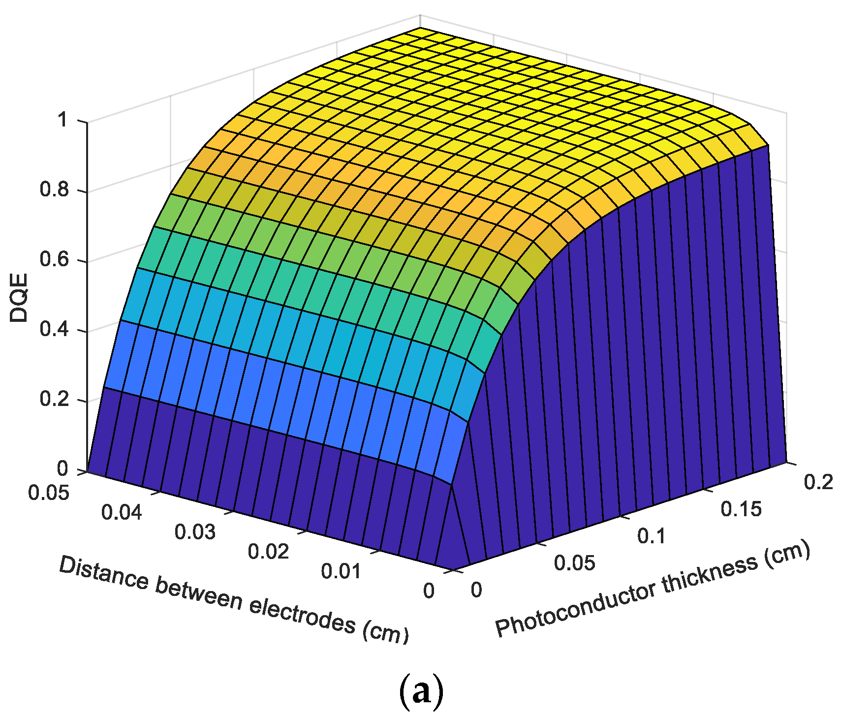
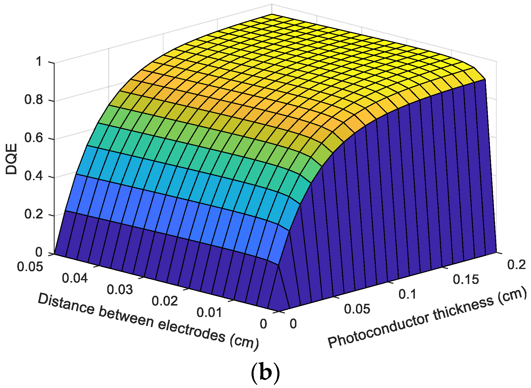
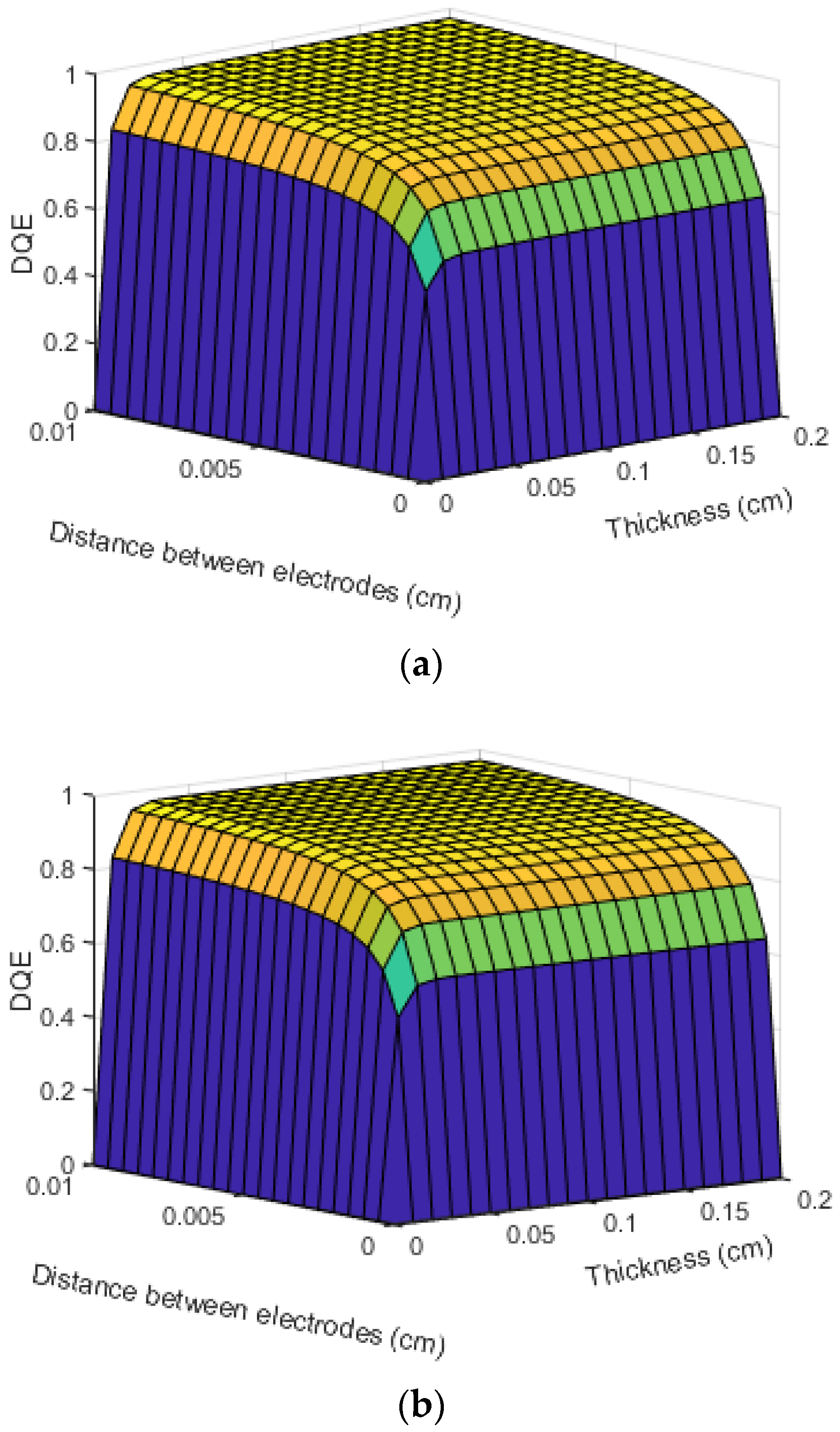
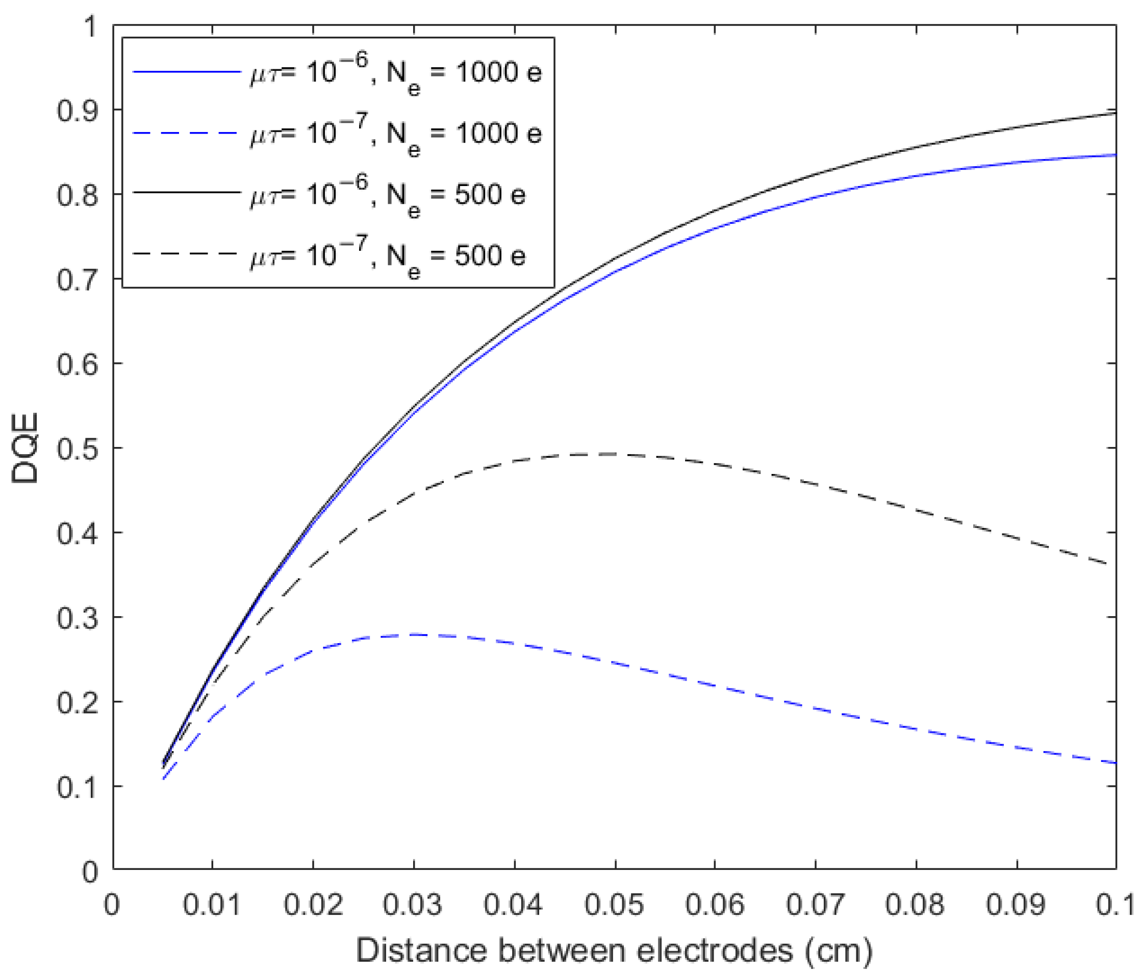
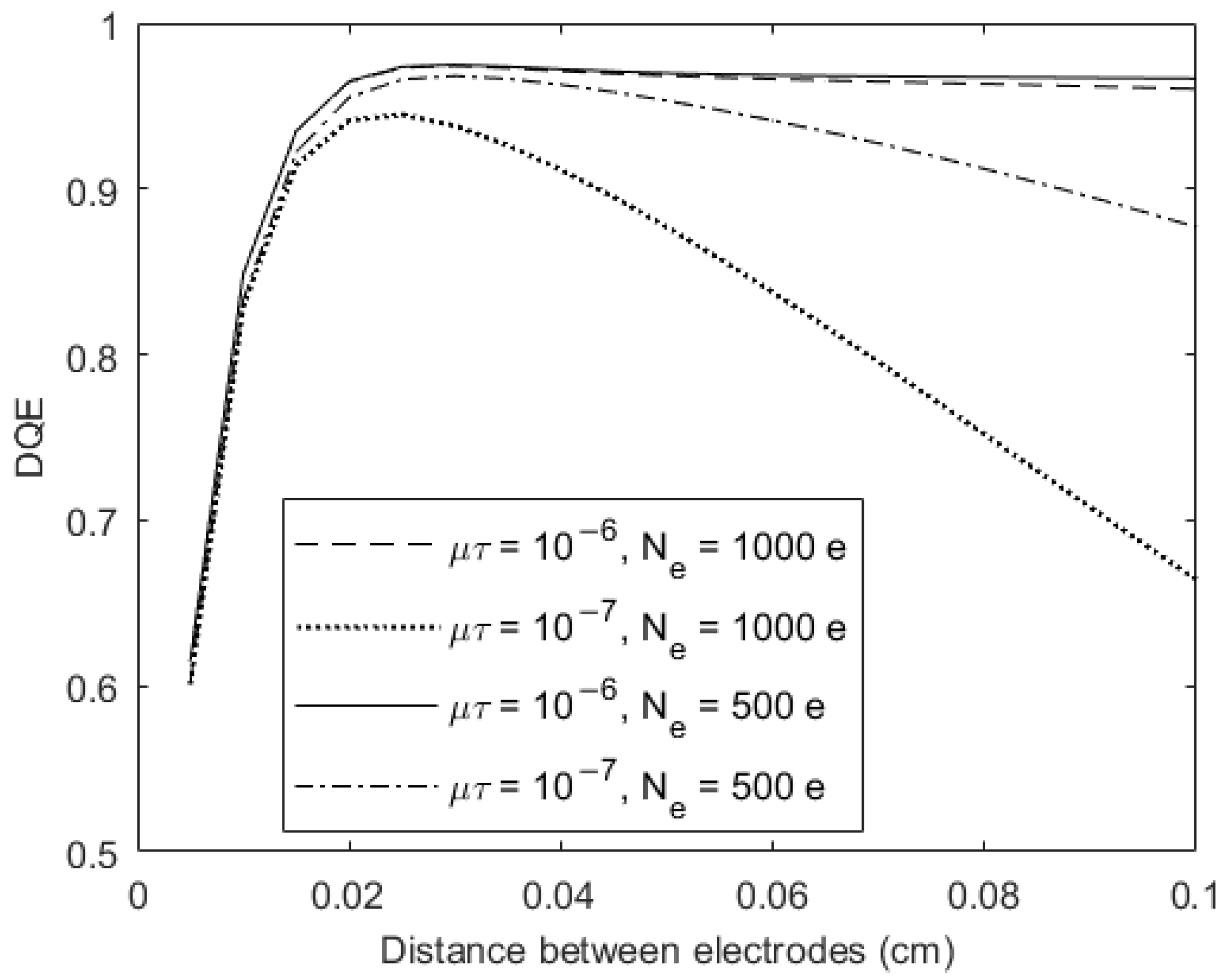
3. Result and Discussion

We have evaluated the DQE performance of poly-MAPbI3 detectors having folded and conventional structures for both fluoroscopy and mammography applications. The thickness of the electrode in the folded structure is assumed to be dfoil = 2.8 μm [13]. The electric field has been taken to be F = 1 V/μm. The average photon energies for fluoroscopy and mammographic applications are assumed to be 60 keV and 20 keV, respectively. The range of exposure varies from 0.1 to 10 μR with the mean exposure being 1 μR in Fluoroscopy whereas it varies from 0.6 to 240 mR with the mean exposure being 12 mR in mammography [21].
The carrier transport properties (mobility and lifetime) of electrons and holes are very similar (within one order of magnitude) in perovskite materials [22]. For simplicity, both electron and hole mobility-lifetimes are assumed to be equal in poly-MAPbI3 for theoretical calculations in this paper. We have varied the μτ values from 10−5 cm2/V to 10−7 cm2/V, which are reasonable for poly-MAPbI3 [5]. The pixel size for fluoroscopic image sensors is large and the total electronic noise (Ne) typically varies from 1000 e to 2000 e per pixel whereas it varies from 500 e to 1000 e per pixel in mammographic detectors due to their smaller pixel size and the use of CMOS or active pixel technology [23]. The noise power, SNe = Ne2.
The DQE of a folded structure for fluoroscopy applications as function of photoconductor thickness l and electrode distance d is shown in Figure 5. The exposure X = 1 µR and µτ = 10−6 cm2/V. The pixel area is assumed as d × d. The DQE increases monotonously with increasing the photoconductor thickness. The DQE should increase by increasing the distance between electrodes up to a certain value. Because the pixel area increases by increasing d and thus each pixel receives more signal, which overcomes the adverse effect of electronic noise per pixel. However, the DQE should decrease after a certain value of d when the charge collection efficiency decreases significantly and affects the signal to noise ratio. In Figure 5b, as d increases, the DQE first increases, reaches a maximum value at d = 0.015 cm, and then decreases afterward (d > 0.015 cm).
The optimum values of l and d for maximizing the DQE under various combinations of exposure, electronic noise and µτ are summarized in Table 1. The optimum DQE is more than 0.8 for all the possible combinations except for µτ = 10−7 cm2/V. The optimum value of l varies within a very narrow range, i.e., from 0.06 to 0.1 cm, whereas the optimum value of d varies widely based on different situations.
Figure 6 shows the DQE of a folded structure for mammographic applications. The exposure X = 3 mR, µτ = 10−6 cm2/V. Table 2 shows the optimum values of l and d for maximizing the DQE under various combinations of exposures, electronic noise and µτ. The DQE increases with increasing l and d (up to d = 0.1 cm). The value of l should be greater than 0.01 cm whereas the optimum value d varies widely based on different operating conditions.
The effects of various parameters such as electronic noise, charge carrier transport properties, electric field, detector thickness on DQE performance of conventional structures are explained in previous publications [8,12]. For making a comparison, the DQE performance of conventional detectors for fluoroscopic and mammographic applications are shown in Figure 7. The exposure X = 1 µR and F = 1 V/μm. The DQE increases with increasing d, reaches a maximum value, and then decreases with further increasing d. There exists an optimum detector thickness (note the spacing between the two electrodes and the detector thickness are the same in conventional detector structure) for which the DQE is maximum. However, the optimum detector thickness and the maximum DQE depend on various parameters as evident from Figure 7. For example, unlike folded structure, the DQE can be less than 0.5 for higher electronic noise together with lower µτ values.
In Table 3, we have gathered information about the optimum distance between electrodes d in different conditions in conventional detector structures for fluoroscopic applications. Unlike the folded structure, the optimum DQE for certain combinations of Ne and μτ can be even lower than 0.3, which is unacceptable for medical imaging.
Figure 8 shows the DQE performance of conventional detector for mammographic applications. The optimum detector thickness is in the range of 0.02 to 0.04 cm and the optimum DQE is larger than 0.9. In Table 4, we have gathered information about the optimum distance between electrodes d under various operating conditions in conventional structures for mammographic applications.
From the above discussion, we see that the DQE critically depends on the detector thickness. As a result, the optimum DQE can be even below 0.3 for certain values of material and device parameters in conventional structure. On the contrary, the folded structure provides more design flexibility for achieving high DQE (even higher than 0.7) by adjusting the distance between electrodes without compromising the quantum efficiency. Since the folded structure is more complex than the conventional structure, one should prefer the folded structure if the photoconductor possesses relatively low linear attenuation coefficient for higher energy X-rays together with poor charge carrier transport properties. Although the model has been applied to perovskite materials, this model and analysis can also be applied to other X-ray photoconductors (e.g., a-Se) as well. One can get similar results for other materials if the material possesses similar transport properties. Most of the X-ray photoconductors have quite similar transport properties as described in a recent book chapter [5].
The μτ values of electrons and holes are considered equal but varied quite widely (within two orders of magnitude) in the calculations. One can easily perform the same calculation considering the actual unequal μτ values. The charge collection efficiency will not change very significantly if μτ values of electrons and holes are within one order of magnitude [12] (this is the case in perovskite materials). Therefore, the main findings of this paper (summarised in previous paragraph) will not qualitatively differ.

4. Conclusions

The DQE performance of both folded and conventional detector structures has been analyzed by considering the quantum noise due to random charge carrier trapping in the photoconductor layer in the cascaded linear system model. An analytical expression for the variance of incomplete charge collection in folded structure has also been developed. The optimum values of photoconductor layer thickness l and spacing between electrodes d for maximizing the DQE under various combinations of exposure, electronic noise and µτ have been determined. The folded structure provides design flexibility for achieving DQE higher than 0.7 by adjusting the distance between electrodes while the maximum possible DQE in conventional structure can be even below 0.3 for certain values of material and detector parameters. The DQE model for folded structure in this paper can also be applied to coplanar detector structure if the electric field profile is considered uniform. This model and analysis of this paper can also be applied to other photoconductive detectors (e.g., a-Se detectors) as well.

Author Contributions

Conceptualization, M.Z.K.; Formal analysis, R.R. and M.Z.K.; Funding acquisition, M.Z.K.; Investigation, R.R. and M.Z.K.; Methodology, R.R. and M.Z.K.; Project administration, M.Z.K.; Resources, M.Z.K.; Software, R.R.; Supervision, M.Z.K.; Visualization, R.R.; Writing—original draft, R.R. and M.Z.K.; Writing—review & editing, M.Z.K. All authors have read and agreed to the published version of the manuscript.

Funding

This research was funded by Natural Science and Engineering Research Council of Canada, grant number RGPIN-2019-05472 and the APC was fully waived to the corresponding author (M. Z. Kabir).

Data Availability Statement

The data presented in this study are available in this article.

Conflicts of Interest

The authors declare no conflict of interest.

References

  1. Spahn, M. X-ray detectors in medical imaging. Nucl. Instr. Methods Phys. Res. Sect. A 2013, 731, 57–63. [Google Scholar] [CrossRef]
  2. Rowlands, J.A.; Zhao, W. Towards a digital radiology roadmap. ECS Trans. 2013, 54, 293–303. [Google Scholar] [CrossRef]
  3. Cowen, A.R.; Davies, A.G.; Sivananthan, M.U. The design and imaging characteristics of dynamic, solid-state, flat-panel x-ray image detectors for digital fluoroscopy and fluorography. Clin. Radiol. 2008, 63, 1073–1085. [Google Scholar] [CrossRef] [PubMed]
  4. Schlosser, D.M.; Huth, M.; Hartmann, R.; Abboud, A.; Send, S.; Conka-Nurdan, T.; Shokr, M.; Pietsch, U.; Strüder, L. Direct and indirect signal detection of 122 keV photons with a novel detector combining a pnCCD and a CsI (Tl) scintillator. Nucl. Instr. Meth. Phys. Res. Sect. A 2016, 805, 55–62. [Google Scholar] [CrossRef]
  5. Kabir, M.Z. X-ray Photoconductivity and Typical Large Area X-ray Photoconductors. In Photoconductivity and Photoconductive Materials; Kasap, S.O., Ed.; Wiley & Sons: Chichester, UK, 2022; Chapter 15. [Google Scholar]
  6. Kasap, S.; Frey, J.B.; Belev, G.; Tousignant, O.; Mani, H.; Greenspan, J.; Laperriere, L.; Bubon, O.; Reznik, A.; DeCrescenzo, G.; et al. Amorphous and Polycrystalline Photoconductors for Direct Conversion Flat Panel X-ray Image Sensors. Sensors 2011, 11, 5112–5157. [Google Scholar] [CrossRef] [PubMed] [Green Version]
  7. Yakunin, S.; Sytnyk, M.; Kriegner, D.; Shrestha, S.; Richter, M.; Matt, G.; Azimi, H.; Brabec, C.; Stangl, J.; Kovalenko, M.; et al. Detection of X-ray photons by solution-processed lead halide perovskites. Nat. Photonics 2015, 9, 444. [Google Scholar] [CrossRef] [PubMed]
  8. Kim, Y.C.; Kim, K.H.; Son, D.Y.; Jeong, D.N.; Seo, J.Y.; Choi, Y.S.; Han, I.T.; Lee, S.Y.; Park, N.G. Printable organometallic perovskite enables large-area, low-dose X-ray imaging. Nature 2017, 550, 87. [Google Scholar] [CrossRef] [PubMed]
  9. Deumel, S.; van Breemen, A.; Gelinck, G.; Peeters, B.; Maas, J.; Verbeek, R.; Shanmugam, S.; Akkerman, H.; Meulenkamp, E.; Huerdler, J.E.; et al. High-sensitivity high-resolution X-ray imaging with soft-sintered metal halide perovskites. Nat. Electron. 2021, 4, 681–688. [Google Scholar] [CrossRef]
  10. Li, Y.; Adeagbo, E.; Koughia, C.; Simonson, B.; Pettipas, R.D.; Mishchenko, A.; Arnab, S.M.; Laperrière, L.; Belev, G.; Stevens, A.L.; et al. Direct conversion X-ray detectors with 70 pA cm−2 dark currents coated from an alcohol-based perovskite ink. J. Mater. Chem. C 2022, 10, 1228–1235. [Google Scholar] [CrossRef]
  11. Kabir, M.Z.; Kasap, S. Modulation transfer function of photoconductive X-ray image detectors: Effects of charge carrier trapping. J. Phys. D Appl. Phys. 2003, 36, 2352–2358. [Google Scholar] [CrossRef]
  12. Kabir, M.Z.; Kasap, S. DQE of photoconductive x-ray image detectors: Application to a-Se. J. Phys. D Appl. Phys. 2002, 35, 2735–2743. [Google Scholar] [CrossRef]
  13. Mescher, H.; Hamann, E.; Lemmer, U. Simulation and design of folded perovskite X-ray detectors. Sci. Rep. 2019, 9, 5231. [Google Scholar] [CrossRef] [PubMed] [Green Version]
  14. Hunter, D.M.; Rowlands, J.A. Differences between transient photoconductivity in a-Se sandwich(bulk) and co-planar(interface) structures. J. Mater. Sci. Mater. Electron. 2020, 31, 9114–9125. [Google Scholar] [CrossRef]
  15. Mainprize, J.G.; Hunt, D.C.; Yaffe, M.J. Direct conversion detectors: The effect of incomplete charge collection on detective quantum efficiency. Med. Phys. 2002, 29, 976–990. [Google Scholar] [CrossRef] [PubMed]
  16. Rabbani, M.; Shaw, R.; Van Metter, R. Detective quantum efficiency of imaging systems with amplifying and scattering mechanisms. J. Opt. Soc. Am. A 1987, 4, 895–901. [Google Scholar] [CrossRef] [PubMed]
  17. Cunningham, I. Applied linear-systems theory. In Handbook of Medical Imaging; Beutel, J., Kundel, H.L., Van Metter, R.L., Eds.; SPIE Press: Washington, DC, USA, 2000; Volume 1, Chapter 2. [Google Scholar]
  18. Zhao, W.; Ji, W.G.; Debrie, A.; Rowlands, J.A. Imaging performance of amorphous selenium based flat-panel detectors for digital mammography: Characterization of a small area prototype detector. Med. Phys. 2003, 30, 254–263. [Google Scholar] [CrossRef] [PubMed]
  19. Kabir, M.Z.; Emelianova, E.V.; Arkhipov, V.I.; Yunus, M.; Adriaenssens, G.; Kasap, S.O. The effects of large signals on charge collection in radiation detectors: Application to amorphous selenium detectors. J. Appl. Phys. 2006, 99, 124501. [Google Scholar] [CrossRef]
  20. Kabir, M.Z. Effects of charge carrier trapping on polycrystalline PbO X-ray imaging detectors. J. Appl. Phys. 2008, 104, 074506. [Google Scholar] [CrossRef]
  21. Rowlands, J.; Yorkston, J. Flat panel detectors for digital radiography. In Handbook of Medical Imaging: Volume 1; Beutel, J., Kundel, H.L., Van Metter, R.L., Eds.; SPIE Press: Washington, DC, USA, 2000; Chapter 4. [Google Scholar]
  22. Ball, J.M.; Petrozza, A. Defects in perovskite-halides and their effects in solar cells. Nat. Energy 2016, 1, 16149. [Google Scholar] [CrossRef]
  23. Kabir, M.Z. Basic principles of solid state X-ray radiation detector operation. In Handbook of II–VI Semiconductor-Based Sensors and Radiation Detectors: Volume 3 Sensors—Biosensors and Radiation Detectors; Korotcenkov, G., Ed.; Springer Nature: Cham, Switzerland, 2023; Chapter 1. [Google Scholar]
Figure 1. A conventional detector structure for negatively biased top electrode.
Electronics 12 02976 g001
Figure 2. Cascaded linear system model for a conventional detector structure.
Electronics 12 02976 g002
Figure 3. A folded detector structure where three pixels are shown.
Electronics 12 02976 g003
Figure 4. Cascaded linear system model for the folded structure of Figure 3.
Electronics 12 02976 g004
Figure 5. The DQE of a poly-MAPbI3 folded X-ray detector for fluoroscopic applications. (a) µτ = 10−6 cm2/V, X = 1 µR, Ne = 1000 e, and (b) µτ = 10−6 cm2/V, X = 1 µR, Ne = 2000 e.
Electronics 12 02976 g005aElectronics 12 02976 g005b
Figure 6. The DQE of a poly-MAPbI3 folded X-ray detector for mammographic applications. (a) µτ = 10−6 cm2/V, X = 3 mR, Ne = 500 e, and (b) µτ = 10−6 cm2/V, X = 3 mR, Ne = 1000 e.
Electronics 12 02976 g006
Figure 7. The DQE of a poly-MAPbI3 conventional X-ray detector for fluoroscopic applications. The exposure X = 1 µR and E = 60 keV. The unit of μτ is cm2/V.
Electronics 12 02976 g007
Figure 8. The DQE of a poly-MAPbI3 conventional X-ray detector for mammographic applications. The exposure X = 3 mR and E = 20 keV. The unit of μτ is cm2/V.
Electronics 12 02976 g008
Table 1. The optimum values of l and d for maximizing the DQE under various combinations of exposure, electronic noise and µτ of a folded poly-MAPbI3 X-ray detector for fluoroscopic applications. The average photon energy E = 60 keV.
X = 0.1 μRX = 10 μR
Electronic Noiseμτ
(cm2/V)
l
(cm)
d
(cm)
DQEl
(cm)
d
(cm)
DQE
1000 e10−5>0.070.025–0.5>0.8>0.070.025–0.5>0.8
10−6>0.070.025–0.1>0.8>0.070.025–0.5>0.8
10−7>0.10.0025–0.01>0.8>0.070.025–0.125>0.8
2000 e10−5>0.070.025–0.5>0.8>0.060.025–0.5>0.8
10−6>0.080.0025–0.045>0.8>0.070.025–0.5>0.8
10−7>0.080.0025–0.005>0.7>0.070.0025–0.05>0.8
Table 2. The optimum values of l and d for maximizing the DQE under various combinations of exposure, electronic noise and µτ of a folded poly-MAPbI3 X-ray detector for mammographic applications. The average photon energy E = 20 keV.
X = 0.6 mRX = 240 mR
Electronic Noiseμτ
(cm2/V)
l
(cm)
d
(cm)
DQEl
(cm)
d
(cm)
DQE
500 e10−5>0.010.025–0.5>0.8>0.010.025–0.5>0.8
10−6>0.010.025–0.5>0.8>0.010.025–0.5>0.8
10−7>0.010.0025–0.05>0.8>0.010.025–0.05>0.8
1000 e10−5>0.010.025–0.5>0.8>0.010.025–0.5>0.8
10−6>0.010.025–0.325>0.8>0.010.025–0.5>0.8
10−7>0.010.0025–0.0325>0.8>0.010.025–0.5>0.8
Table 3. The optimum detector thickness for maximizing DQE under various combinations of exposure, electronic noise and µτ of a conventional poly-MAPbI3 X-ray detector for fluoroscopic applications. The average photon energy E = 60 keV.
X = 0.1 μRX = 10 μR
Electronic Noiseμτ
(cm2/V)
d
(cm)
DQEd
(cm)
DQE
1000 e10−50.10.920.10.9307
10−60.090.76430.10.9109
10−70.020.16570.0950.8048
2000 e10−50.10.8890.10.9304
10−60.0650.57280.10.9055
10−70.0150.0610.0650.6335
Table 4. The optimum detector thickness for maximizing DQE of a conventional poly-MAPbI3 x-ray detector for mammographic applications under various combinations of exposure, electronic noise and µτ. The average photon energy E = 60 keV.
X = 0.6 mRX = 240 mR
Electronic Noiseμτ
(cm2/V)
d
(cm)
DQEd
(cm)
DQE
500 e10−50.050.99840.050.9987
10−60.030.97390.030.9751
10−70.0250.93790.060.9812
1000 e10−50.050.99750.060.9986
10−60.030.97050.030.9751
10−70.0150.87380.040.9804
Disclaimer/Publisher’s Note: The statements, opinions and data contained in all publications are solely those of the individual author(s) and contributor(s) and not of MDPI and/or the editor(s). MDPI and/or the editor(s) disclaim responsibility for any injury to people or property resulting from any ideas, methods, instructions or products referred to in the content.

