Review

A Review on Direct Digital Conversion Techniques for Biomedical Signal Acquisition

1
College of Information Science and Electronics Engineering, Zhejiang University, Hangzhou 310027, China
2
School of Micro-Nanoelectronics, Zhejiang University, Hangzhou 310027, China
3
Institute for Integrated Micro & Nano Systems, School of Engineering, University of Edinburgh, Edinburgh EH8 9JU, UK
*
Author to whom correspondence should be addressed.
Electronics 2023, 12(12), 2676; https://doi.org/10.3390/electronics12122676
Submission received: 8 May 2023 / Revised: 5 June 2023 / Accepted: 9 June 2023 / Published: 15 June 2023
(This article belongs to the Special Issue Advanced Analog Circuits for Emerging Applications)

Abstract

:
Biomedical signals such as Electrocardiogram (ECG), Electroencephalogram (EEG) and photoplethysmography (PPG) are recorded routinely to provide helpful information for early diagnosis of disease. Low power consumption is very important to allow long-term ambulatory monitoring with battery-powered systems. A direct digital conversion (DDC) technique has been proposed in recent years, which employs preamplifier and data converters, reducing the complexity of the readout chain and thus its power consumption. This paper provides a review on DDC for biopotential signals and bio-optical signal acquisition. The state-of-the-art DDC-based readout architectures together with circuit implementations are provided.

1. Introduction

Home-based health monitoring through wearable devices is becoming prevalent. Low power consumption is very important to allow long-time monitoring. Besides power consumption, for multiple-channel applications such as neural recording, there are also requirements of a small size and minimum off-chip components.
There are mainly two categories of biomedical signals: biopotential signals such as Electrocardiogram (ECG) and Electroencephalogram (EEG), and bio-optical signals such as photoplethysmography (PPG) and near infrared spectroscopy (NIRS). Interestingly, they share a similar signal pattern, which is a small useful component superposed on a large quasi-DC component [1]. Traditional biopotential signal readouts consist of an AC-coupled preamplifier followed by an analog-to-digital converter (ADC) [2]. To reliably achieve a sub-Hz high pass frequency, large off-chip components are needed. Meanwhile, DC-coupled structures have a limited gain, reducing the effective resolution on the useful AC signal at the ADC output. Traditional bio-optical signal readout circuits use an integrator or a transimpedance amplifier (TIA) to convert the photocurrent to a voltage that is then digitized by an ADC [3]. However, the architecture of using TIA is prone to noise folding. In addition, due to the low perfusion index (PI) of the chest PPG signal, a larger dynamic range (DR) is required for the readout circuit, which undoubtedly increases the complexity of the design and power consumption.
In recent years, a direct digital conversion (DDC) structure has been proposed to directly digitize biomedical signals, which overcomes the above problems by combining preamplifier and ADC into one stage while making compromises among area, noise, power, and input impedance, etc.
In Section 2, we describe the techniques for neural signal recording. In Section 3, the techniques for voltage-controlled oscillator-based signal recording are presented. In Section 4, we discuss the techniques for PPG/NIRS signal recording. In Section 5, we conclude with the focus of neural signal recording and PPG/NIRS signal recording.

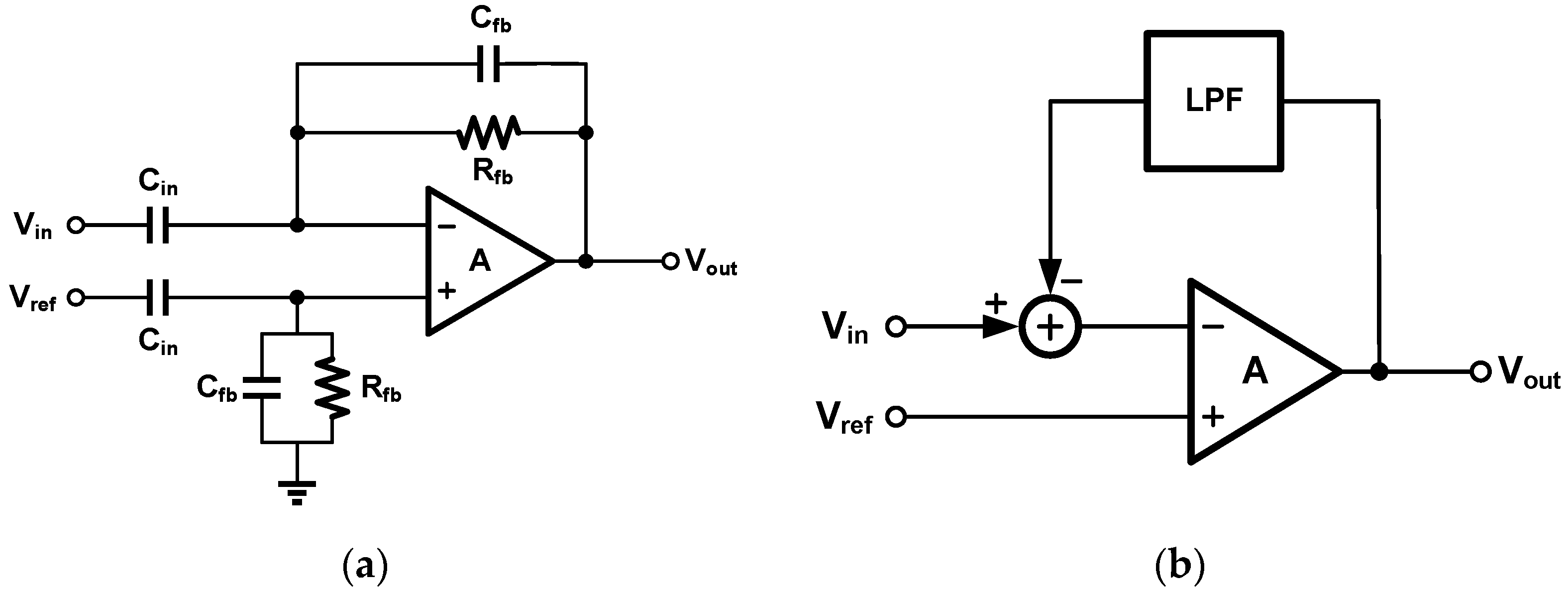
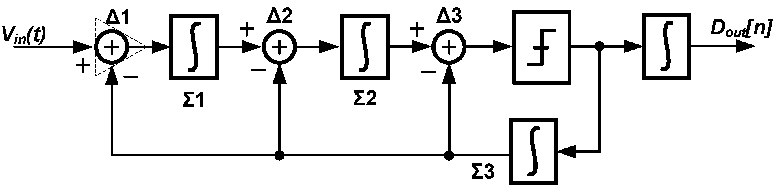
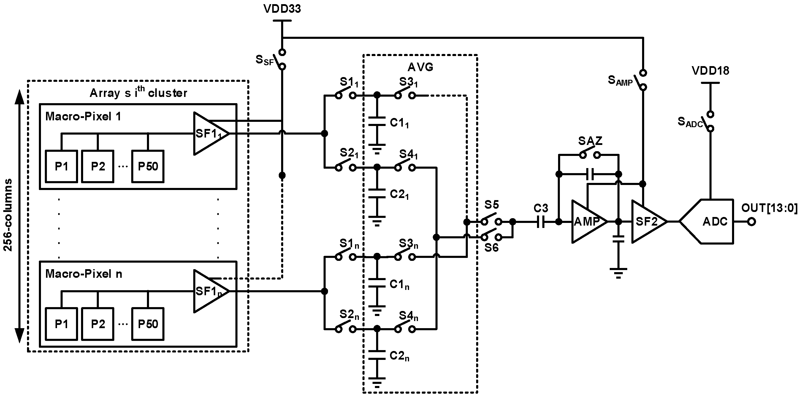
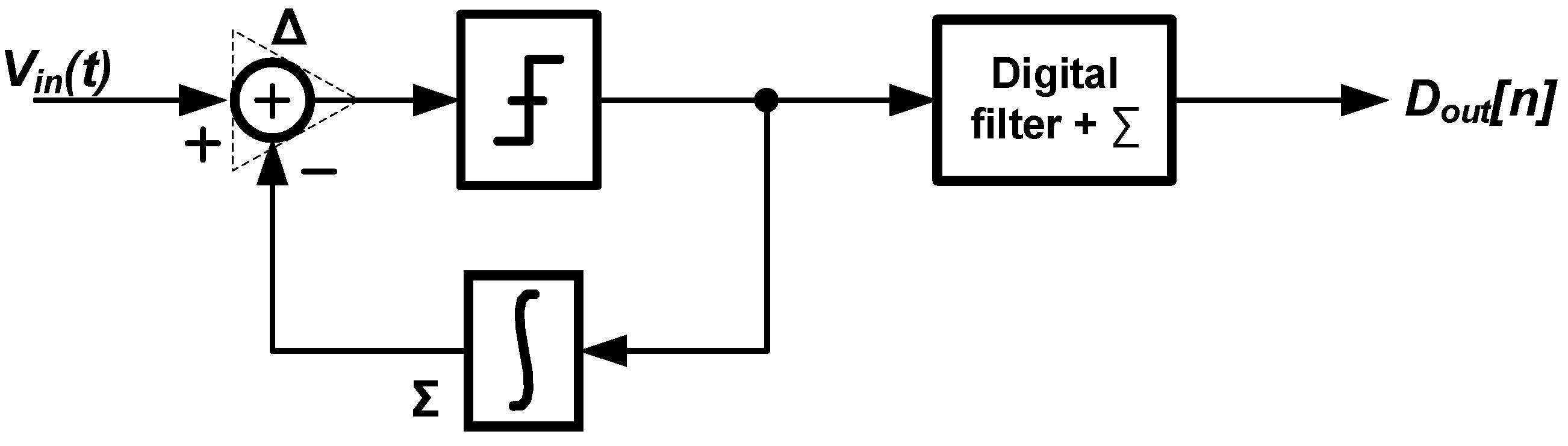
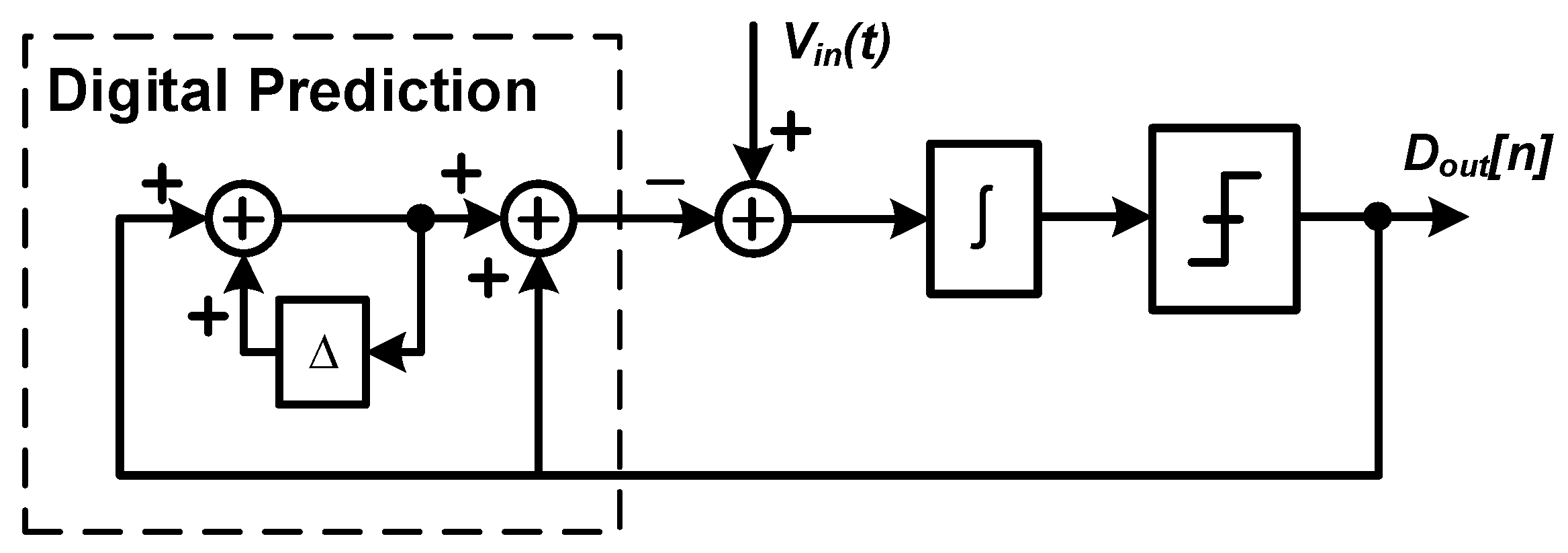
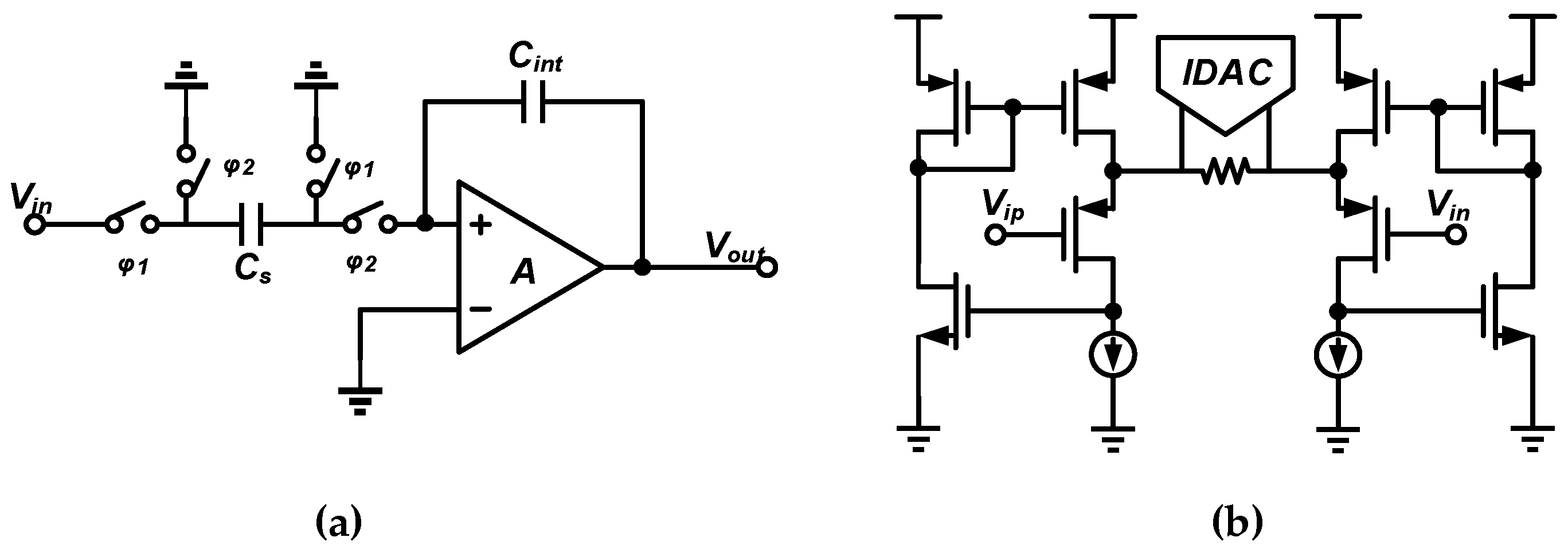
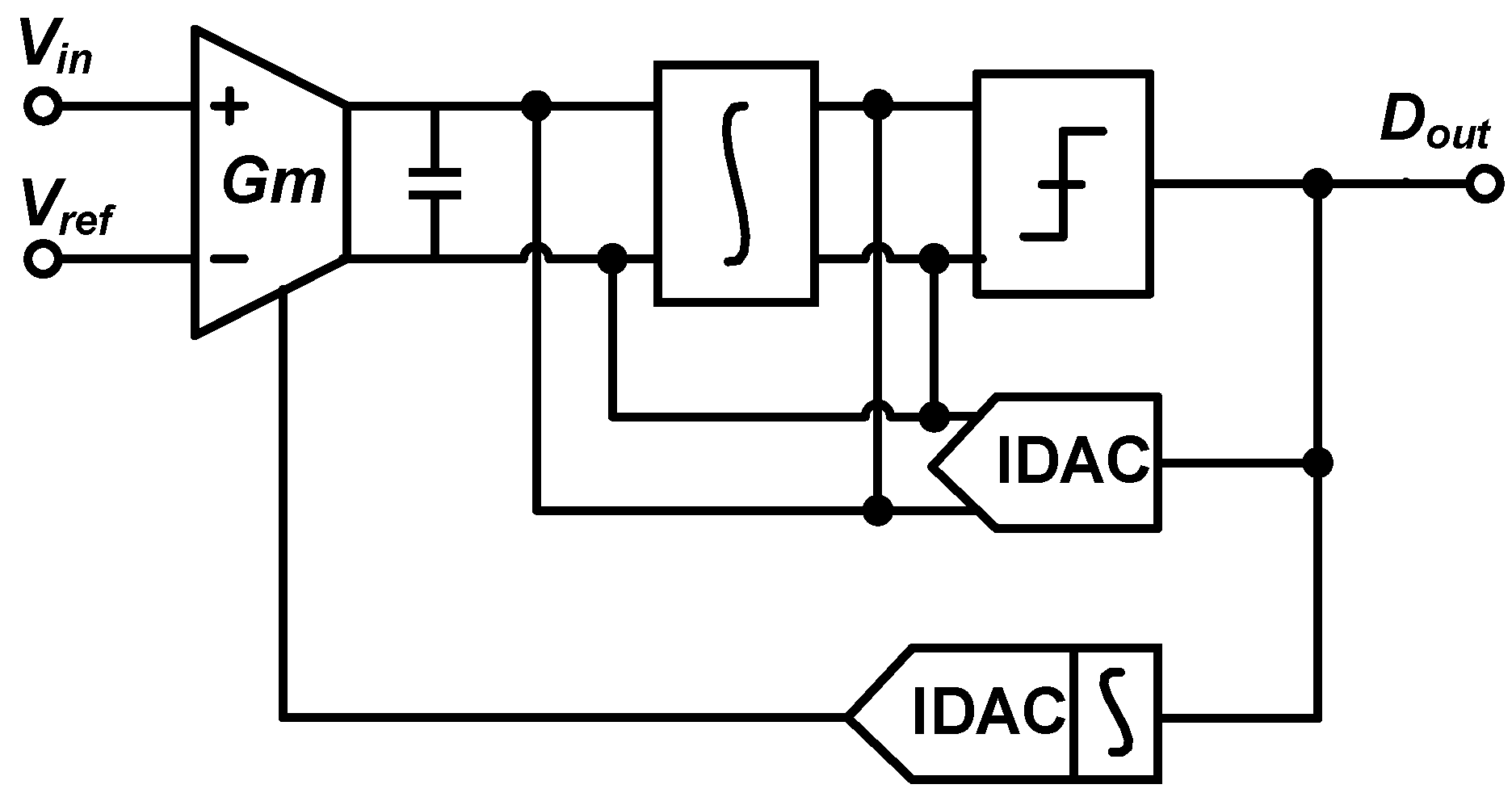
2. Techniques for Biopotential Signal Recording

Multi-electrode neural recordings are becoming standard practice in neuroscience research to gain knowledge on the way the brain works and enable neuro-prosthetic applications. There is a clear need for a higher number of recording sites per given area, which provides real-time signals at the level of neurons from an ever-increasing brain volume. In parallel with the requirements of signal integrity and low power consumption, a miniature IC chip area with the minimum number of off-chip component is of paramount importance to enable hundred-channel neural probes [4].
One of the main issues leading to a large chip area is the electrode DC offset originating from the electrode–electrolyte interface [5]. This offset can reach the levels of up to 100 mV depending on the type of material of the electrode and the surrounding tissue and fluids [5], which is higher than the actual neural signals, i.e., action potential (AP) around 1 mV and local field potential (LFPs) around 10 mV. While accepting this large DC offset would lead to a limited gain of frontend amplifier and very high resolution of ADC with high power, the common solution is to reject the DC component with a passive or active filter, as shown in Figure 1.
The high pass corner frequency can be expressed as fHP = 1/2πRfbCfb. With the properly chosen Rfb and Cfb, the filter cut-off should be made under 1 Hz to capture the complete signal band of the LFPs while rejecting the DC signal. In terms of circuit design, this approach may be challenging because high product Rfb●Cfb requires high values for one or both of the filter elements. Achieving both high capacitance capacitor and high resistance resistor values requires a large circuit area. Pseudo-resistors, as shown in Figure 2 (n is design parameter and UT is the thermal voltage), can be used with a small area, but it can exhibit an X0.1 to X10 variation over PVT and be sensitive to light exposure [6]. The direct digital conversion technique can provide DC rejection capability with an extremely small chip area.
To the best of the authors’ knowledge, the first DDC for biopotential signal readout was proposed by H. Kassiri et al. [7]. Figure 3a shows a conventional first-order ∆∑ ADC; this circuit has a tradeoff between integrated noise, oversampling rate (OSR), and power consumption. As a result, with an anticipatory design, it can satisfy a neural recording front-end requirement of bandwidth, noise, and power. However, any DC offset from the electrode can make the amplifier saturated.
In order to improve the suppression of the electrode DC offset (EDO) while maintaining a high chain gain, the so-called ∆2∑structure added an additional ∆ stage to the ∆∑modulator as shown in Figure 3b. As a result, the difference of two consequent input signals is fed into the DDC, which removes the DC component, avoiding integrator saturation. The output of the quantizer is thus the derivative of the input signal, and it can be integrated into the digital domain to reconstruct the AC component of the original signal. In the feedback path, the DAC and integrator is implemented by a digital controlled charge pump. Although this structure enables EDO rejection in a rail-to-rail range, integration using IDAC results in an insufficient ability to track fast transients due to the large time constant of the integrator. Moreover, a DT ∆2∑ADC needs a high OSR to avoid KT/C noise aliasing at the cost of limited input impedance. As a result, the differential-mode signal caused by different high impedances of the microelectrode attenuates the ability of immunizing large artifacts.
Figure 4 shows an op-amp-less ∆-modulator diagram using a continuous-time ∆-ADC [8] to achieve the shaping the spectra of neural signals such as LFPs and ECoG, which can decrease the DR requirement of recording front end by more than 30 dB. Meanwhile, this structure achieves above GΩ input impedance because it uses the DC-coupled front end without input capacitors. However, without noise shaping, low-frequency noise of the system is high, so that SNDR is limited.
A second-order hybrid continuous time to discrete time (CT-DT) ∆∑-∑modulator [9] was presented as shown in Figure 5. The structure adds a ∑ stage to a conventional two-order ∆∑-modulator, thus achieving three-stage noise shaping and one-stage input signal shaping. Therefore, by considering calculation and design, this architecture can offer a good tradeoff between input range, EDO cancelation, noise and linearity. In addition, to ensure the input impedance in case of using chopping, an auxiliary input impedance boosting path is implemented. However, the realized input impedance is only 34 MΩ. A simple digital accumulator is used to obtain fast recovery from large motion artifacts (MA). This structure can simultaneously suppress EDO and an MA of >300 mV. However, the linearity of the system is limited due to the use of a five-bit quantizer and capacitive digital-to-analog converter (CDAC).
C. Kim proposed another second-order hybrid DDC architecture [10] as shown in Figure 6. This system connects the biopotential signal directly to the second integrator which is implemented in continuous time and moves the sampling to the comparator to avoid sampling noise kT/C. Similar to [7], this structure uses predictive digital auto-ranging (PDA) for high-input-dynamic range and avoiding the need for substantial gain attenuation. Moreover, PDA substantially improves transient response to large artifacts, tracking full-swing signal excursions without saturation while quickly reestablishing noise-limited resolution upon the settling of the signal. Finally, fast transient recovery of 200 mV/ms is achieved with a 90 dB input dynamic range, less than 1 µVrms input-referred noise from DC to 500 Hz, at a 0.8 µW power consumption, and with a 0.024 mm2 area. However, the input impedance of this work is still relatively low (26 MΩ).
Works [7,9,10] employed switched cap/chopping circuit at the input as shown in Figure 7a, which leads to a limited input impedance. Recently, Gm-C-based structures have been proposed to solve this problem. S. Wang exploited the current feedback gm stage [11] as the CT-integrator within a ∆2∑ architecture [12], which is shown in Figure 7b. The inherent high Zin of the gm stage together with the proposed bootstrapping increase the input impedance to 663 MΩ, which is shown in Figure 8. The EDO rejection of this work is, however, only ±70 mV. M. Sporer proposed a Gm-C-based second-order delta sigma modulator in [13] using bulk-driven DSL. The structure achieves a bandwidth of 10 kHz and an input impedance of 238 MΩ, while the EDO rejection range is only ±100 mV. A similar structure was proposed in [14]; however, its linearity is limited due to the open-loop Gm-C stage. Readout circuits in other fields [15,16] can also offer some ideas. An energy-efficient readout IC [15] achieves 133 dB SNR and 134 dB CMRR, which consists of a CCIA driving a CT-∆∑M. In [16], a CT-integrated readout interface was presented for inertial sensors with high energy efficiency and high resolution.
Table 1 summarizes the performance of state-of-the-art DDC-structured biopotential readout circuits. In [7], a DT ∆-∆∑ structure was implemented to eliminate the input DC offset, which achieved rail-to-rail offset tolerance. A high OSR (1000) is needed to reduce kT/C noise. Such high switch frequency with a capacitor leads to a limited input impedance (<100 MΩ). In [9], a hybrid CT-DT ∆∑-∑ modulator was used which achieves three-stage noise shaping. The low-gain (gain = 8) stage needs large power consumption (15 μW) to reduce input-referred noise. The system linearity is limited by a five-bit quantizer and a five-bit CDAC. In [10], another second-order hybrid DDC architecture was proposed which connects the input signal to the second integrator avoiding kT/C noise. This work implemented a PDA for high input range, avoiding the requirements of gain. Therefore, the system offers a good tradeoff between noise (<1 µVrms) and input range (90 dB). However, the input impedance is still relatively low (26 MΩ). In [8], an op-amp-less ∆-modulator was proposed which achieves spectra shaping of low-frequency signals to relax the DR requirement. This work has an above GΩ (2.94 GΩ) input impedance because there are no input capacitors. Without an op-amp, the system only occupies 0.044 mm2. However, without noise shaping, SNDR (60 dB) is limited. In [12], a current feedback gm stage was proposed as the CT-integrator within a ∆2∑ architecture. A second-order noise shaping (OSR = 512) was used to achieve low quantization noise. However, the flicker noise of current mirror was not chopped, so that the noise (2.88 µVrms) of the system was not low enough. In order to boost input impedance, this work implemented bootstrapping first gm stage, which limited EDO tolerance (70 mV). In [13], a Gm-C-based second-stage ∆∑-modulator was used with bulk-driven DSL. It achieved a 238 MΩ input impedance with low OSR (136) and small input capacitor (60 fF). In [14], a similar structure was used, achieving low noise (3.9 µVrms) with a 0.0046 mm2 area.
Overall, compared to the DT delta-sigma DDC structure, the CT (continuous-time) delta-sigma DDC structure is more favored in neural signal acquisition systems because it does not require a high oversampling ratio and hence avoids noise aliasing. If a large input range is the primary requirement of the system, the preferred approach is to use low gains and ∆∑-∑ structures [10]. When input impedance is of paramount importance, a system that does not use a large input capacitance becomes the primary choice [8,12]. When considering the number of acquisition channels limited by chip area, using the Gm-C structure without capacitors as an integrator has advantages, as demonstrated in [13,14].

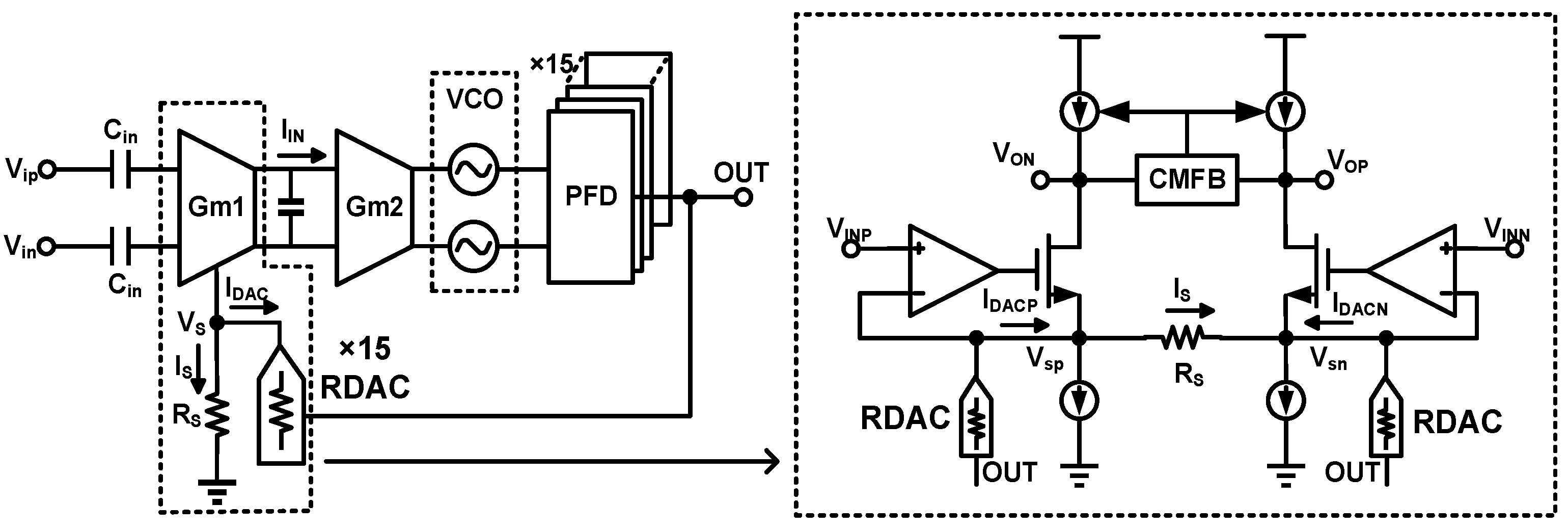
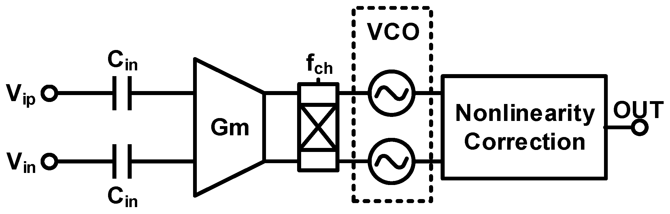
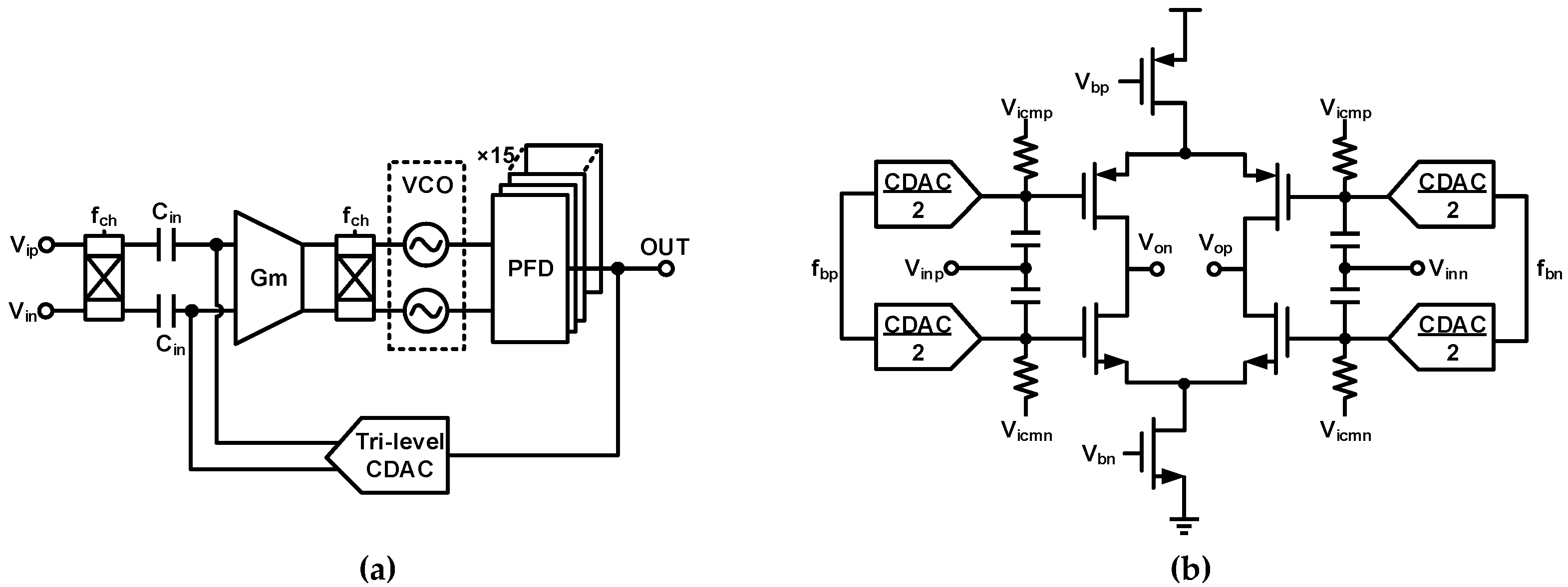
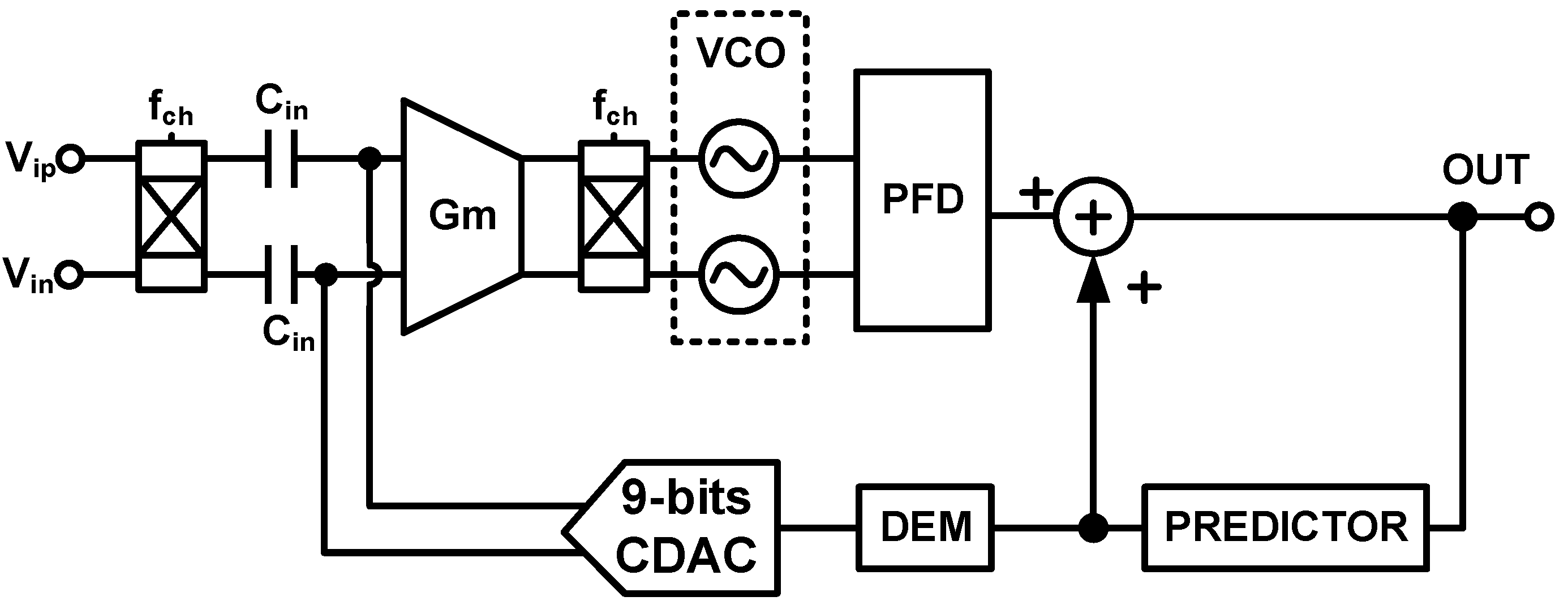
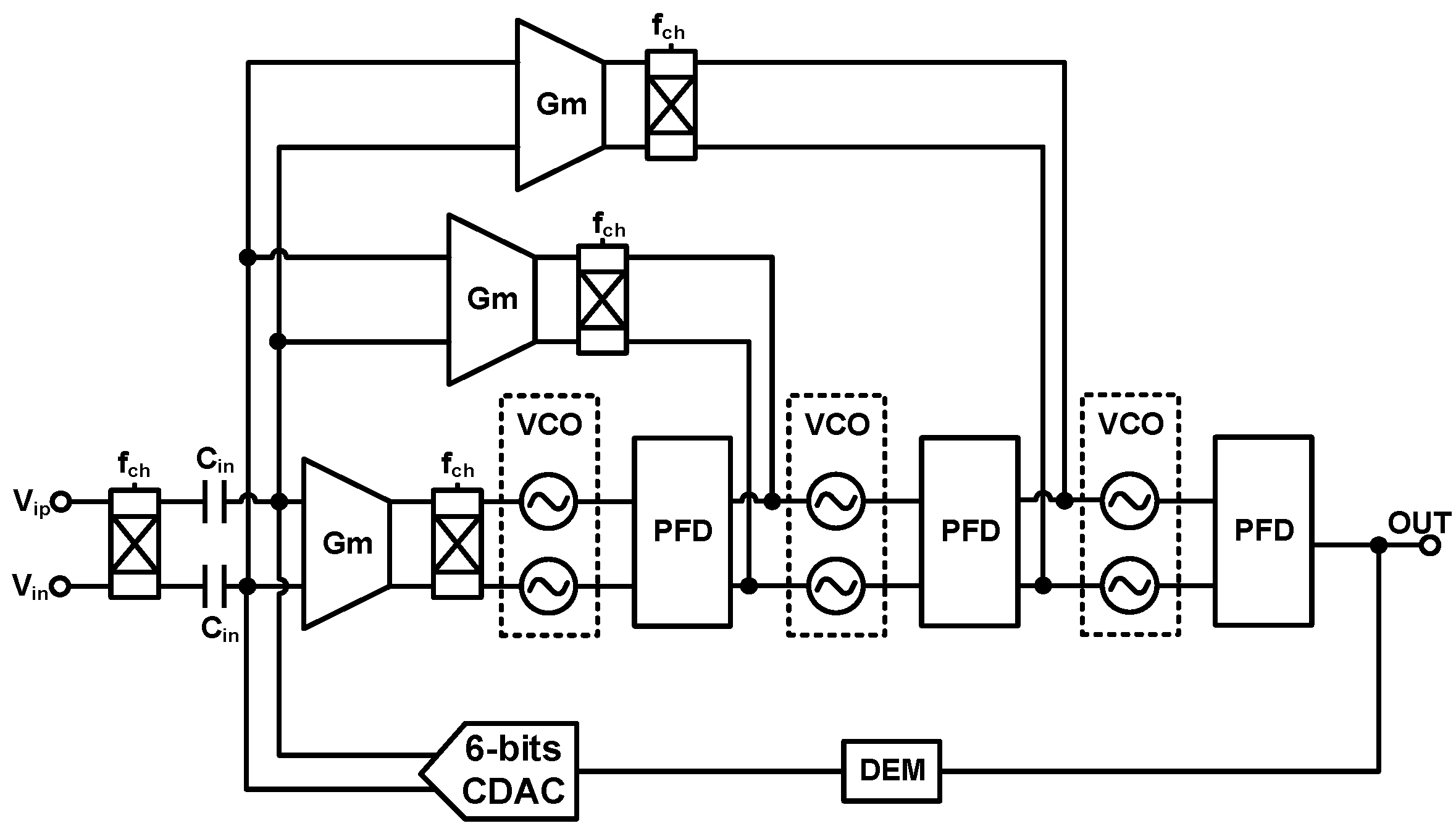
3. Techniques for Voltage-Controlled Oscillator (VCO)-Based Signal Recording

Although the CT-∆∑modulator achieves a high dynamic range, low noise and high input impedance at the same time, the supply voltage cannot be easily reduced to a sub-1V range because the output signal amplitude and thus the overall SNR/SNDR are always limited by the supply. This makes the front ends difficult to implement in a more advanced technology node together with the ever-complicated digital processing circuits, which benefit significantly from Moore’s law. Frequency-domain separation is a workable approach to reduce supply and cancel artifacts [17].
Therefore, W. Jiang proposed a VCO-based neural signal recording system [18] in 2017 which is able to work at a 1.2 V supply while providing similar performance as that of the CT-∆∑ architecture. Instead of processing input signal in the voltage domain, it directly converts voltage into the frequency domain by using VCO. Due to the high voltage-to-frequency gain of VCO, the input signal can be applied directly to the VCO without preamplifier, as shown in Figure 9, achieving a high input range together with low noise. To maintain high SDNR of system, the VCO nonlinearity can be corrected by foreground correction. In this work, it is implemented by a fifth-order polynomial VCO tuning curve stored in the digital circuits. The VCO-based neural signal recording system achieves a ±50 mV input range and a 76 dB SNDR. Meanwhile, it occupies 0.135 mm2 with an analog power of 3 µW and a digital switching power of 4 µW. The disadvantage of this loop architecture is that it may still limit the linearity of system because of PVT variations, even with a nonlinearity calibration effort.
To avoid this limitation of open-loop VCO-based system, a closed-loop CC-VCO-based sensor readout system featuring hybrid PLL-∆∑modulator is proposed in [19]. As shown in Figure 10, the dual VCOs integrate the input voltage to create phase variation, which is subsequently detected by phase frequency detector (PFD). The PFD acts as an integrator that generates the sum of input phase difference. Compared to classic PLL, this work uses an array of 15 PFDs instead of only one PFD as an efficient quantizer. The dual VCO structure allows the PFD to perform self-comparison without an extra phase. The PFD array can detect every delay stage of VCOs which naturally create a set of evenly phase-shifted PWM waveforms without a classic barrel-shifter. Thus, by sampling the PFD array, the quantized phase difference can directly be regarded as output and CDAC control signal. The use of all VCO phases allows low VCO frequency without information loss, which avoids high-speed VCO to save power and area. The prototype readout system achieves a 78 dB SNDR in 10 kHz BW, consuming 4.5 μW and a 0.025 mm2 active area with a 172 dB FoM. Although this work has an excellent tradeoff between power, area, input range and noise, the input impedance is reduced since a chopper is applied.
Jiannan Huang proposed a ΔΣ-modulator structure using a VCO-based quantizer [20] while avoiding the drawback of nonlinearity by applying differential pulse code modulation (DPCM). As shown in Figure 11, the predictor is designed to exploit the correlation between the adjacent sample of the input signal so that the quantizer only needs to deal with the remaining prediction error. It allows reducing the nonlinearity of the VCO quantizer by lowering the signal swing at the input of the VCO quantizer. In addition, oversampling increases the correlation between the adjacent sample of the input signal, so a high oversampling rate (OSR) leads to a good linearity of the VCO system. This sensor front end consumes 3.2 µW of power and achieves an SNDR of 89 dB and a DR of 94 dB in 500 Hz of bandwidth. Together with a 1.18 µVrms integrated input-referred noise, it achieves a noise efficiency factor (NEF) of 4 and a Schreier FoM of 171 dB. Despite the fact that other indicators are excellent, a nine-bit CDAC is needed to feedback prediction signal, leading to extra area; in addition, input impedance is limited by chopping frequency and input capacitance.
Corentin Pochet proposed a third-order VCO-based ΔΣADC [21] using a pseudo-virtual ground feedforward technique. As shown in Figure 12, each integrator is comprised of a Gm stage and VCO followed by PFD. The pseudo-virtual ground of the ADC feeds forward to the second and third integrators using Gm cells. The signal summation between the feedforward path and the integration path is performed in the current domain, and the resulting current drives the CCO of the next integrator. With third-order shaping, the system achieves a 1.8 V input range, a 92.1 dB SNDR over a 2.5 kHz bandwidth and consumes 4.4 μW with a 0.1 mm2 area. However, the input impedance is still poor since a chopper is used.
To avoid impairing input impedance, work [22] presents a highly linear Gm-C-based CT-DSM (delta-sigma modulator) without chopping. As shown in Figure 13, a resistive feedback DAC (RDAC) is implemented in parallel with resistor RS of first Gm-C integrator instead of CDAC. The signal current IS through RS and the feedback current IDAC generated by RDAC are subtracted at the VS. Due to the feedback-assisted Gm linearization, the magnitude of the IIN maintains within the LSB of the feedback DAC current even with a large input voltage, which can significantly improve the linearity of the CTDSM system. This design achieves a high input impedance, a 300 mVpp linear input range, a 80.4 dB SNDR, a 81 dB DR and consumes only 6.5 µW with a signal bandwidth of 10 kHz. However, without chopping, this system has poor CMRR and the schematic of first Gm-C integrator is complex.
In [23,24], several methods to save power and reduce noise for VCO-based modulators are provided. In [23], a modulation method is described for spread-spectrum clock generators (SSCGs) which reduce clock power. In [24], a noise reduction method for ∆∑ bang-bang PLL is presented. Table 2 summarizes the performance of state-of-the-art VCO-based DDC-structured biopotential readout circuits. In [18], a VCO-based neural recording system which works at 1.2 V supply is proposed. This work achieves good performance on SNDR (76 dB) compared with a conventional delta-sigma modulator. However, the linearity of the system depends on PVT variations of the calibration module. In [19], a closed-loop VCO-based system is presented using a PFD array as quantizer. With a PFD array, the system avoids high-speed VCO to save power (4.5 μW) and area (0.025 mm2). Therefore, the FoM of the system is higher than that in [18]; however, the input impedance is not considered. In [22], a Gm-C-based CT-DSM is proposed without chopping. This work has good performance on SNDR (80.4), area (0.078 mm2) and input impedance (13.3 MΩ@10 kHz). However, without chopping, the CMRR (76 dB) and noise (95 nV/√hz) are poor. In [20], a VCO-based quantizer is proposed using DPCM to avoid nonlinearity. With low OSR (OSR = 32), the system achieves an SNDR of 89 dB, consuming 3.2 μW. Although other performance values are excellent, the input impedance (4 MΩ) is limited by the chopper and input capacitor. In [21], a third-order VCO-based DSM was proposed using a pseudo-virtual ground to eliminate the large swing at the integrator output. This work also achieves good tradeoff between SNDR (92 dB) and power (4.4 μW), but input impedance is poor.
Compared to the traditional DDC structure, the VCO-based DDC structure can achieve higher SNDR and FOM more easily because it has larger input range and displays lesser quantizer power consumption. The linearity of closed-loop structures is better [19,20,21,22] compared to the open-loop VCO-based structures in [18]. An obvious advantage of higher-order VCO-based DDC [21] is their ability to achieve large input range and high SNDR. When input impedance is the primary requirement, chopper-less designs [18,22] exhibit excellent performance at the cost of low-frequency noise. When considering the area of the acquisition chip, the hybrid PLL DSM structure proposed in [19] is suitable due to its low VCO center frequency.

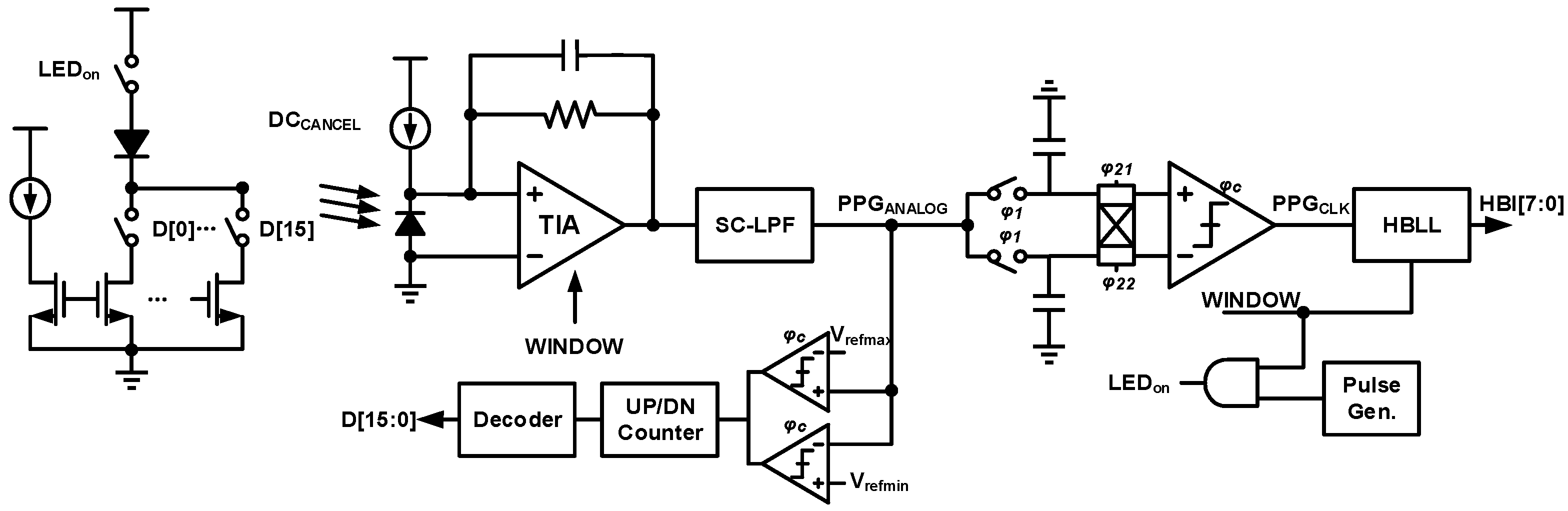
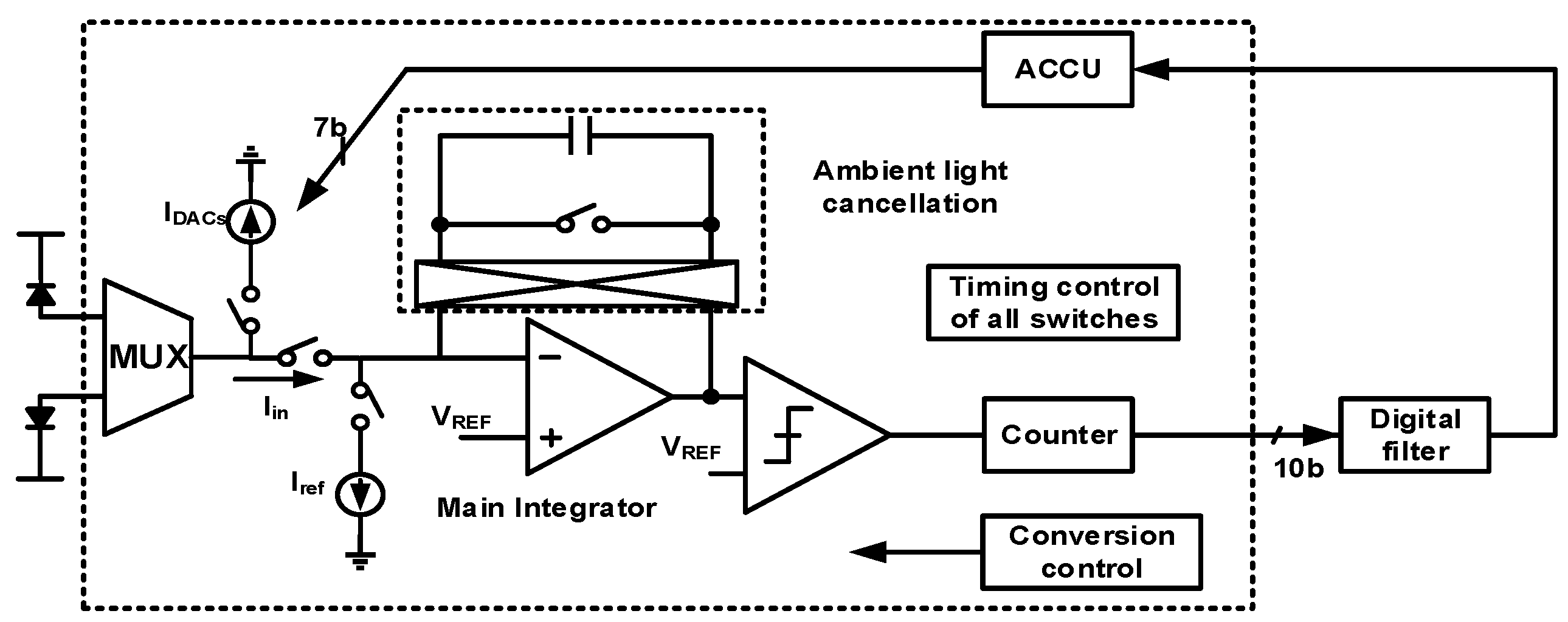
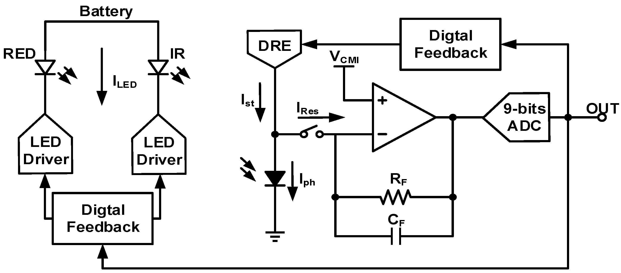
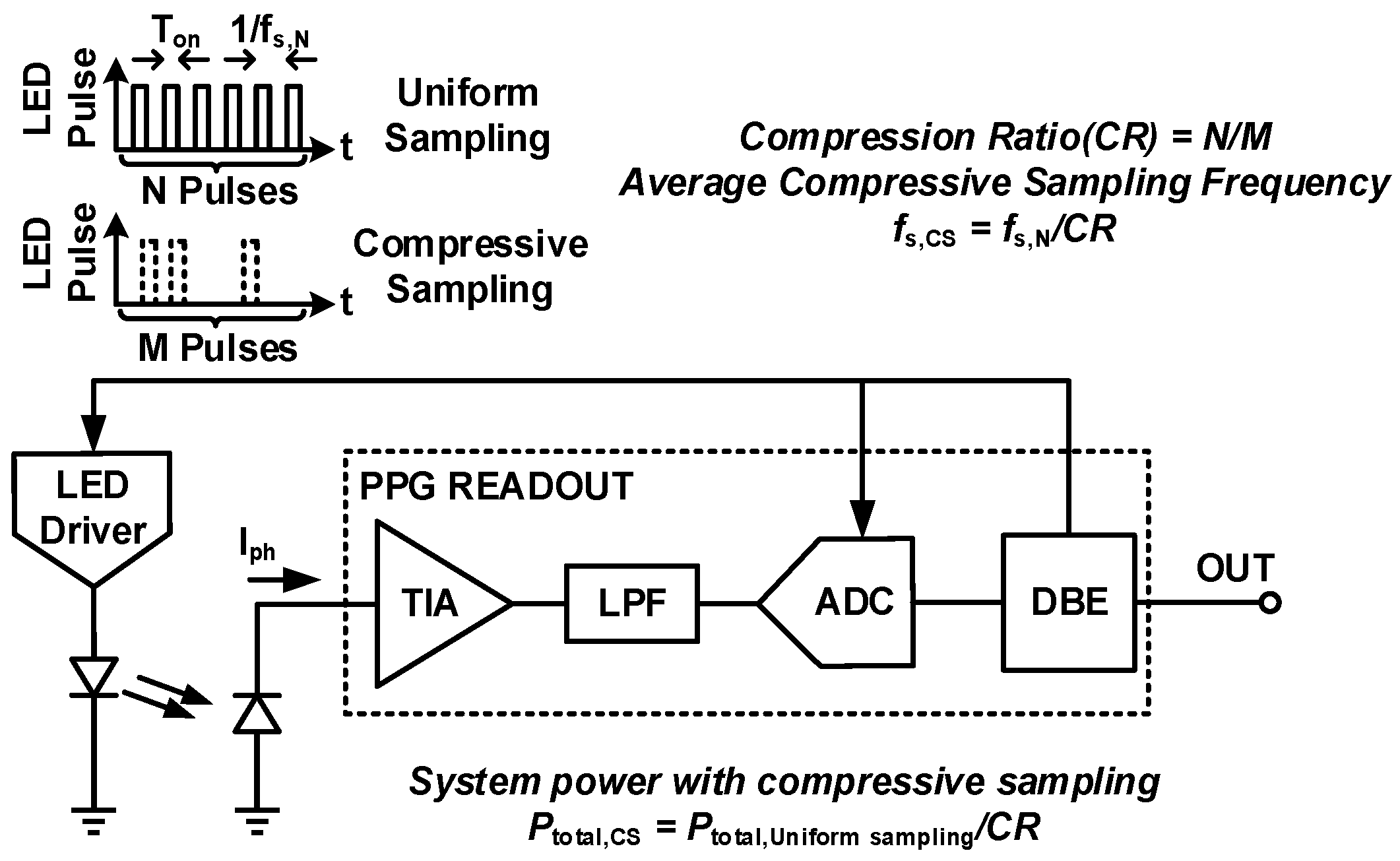
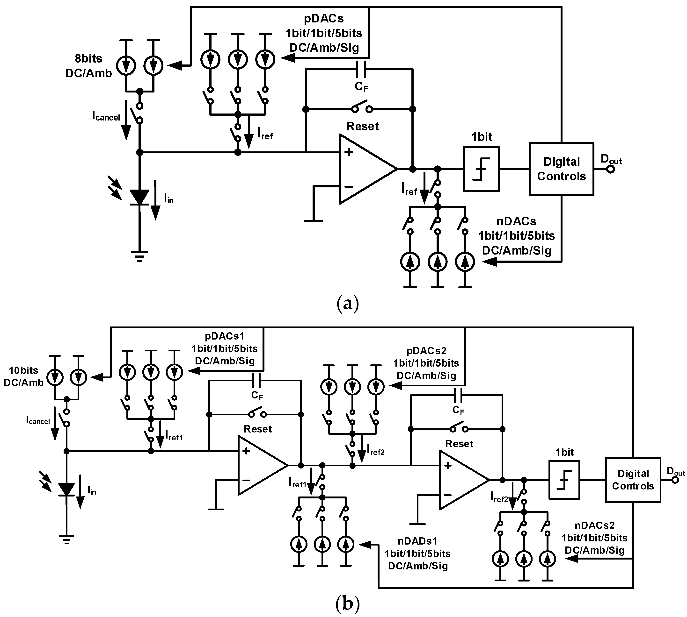
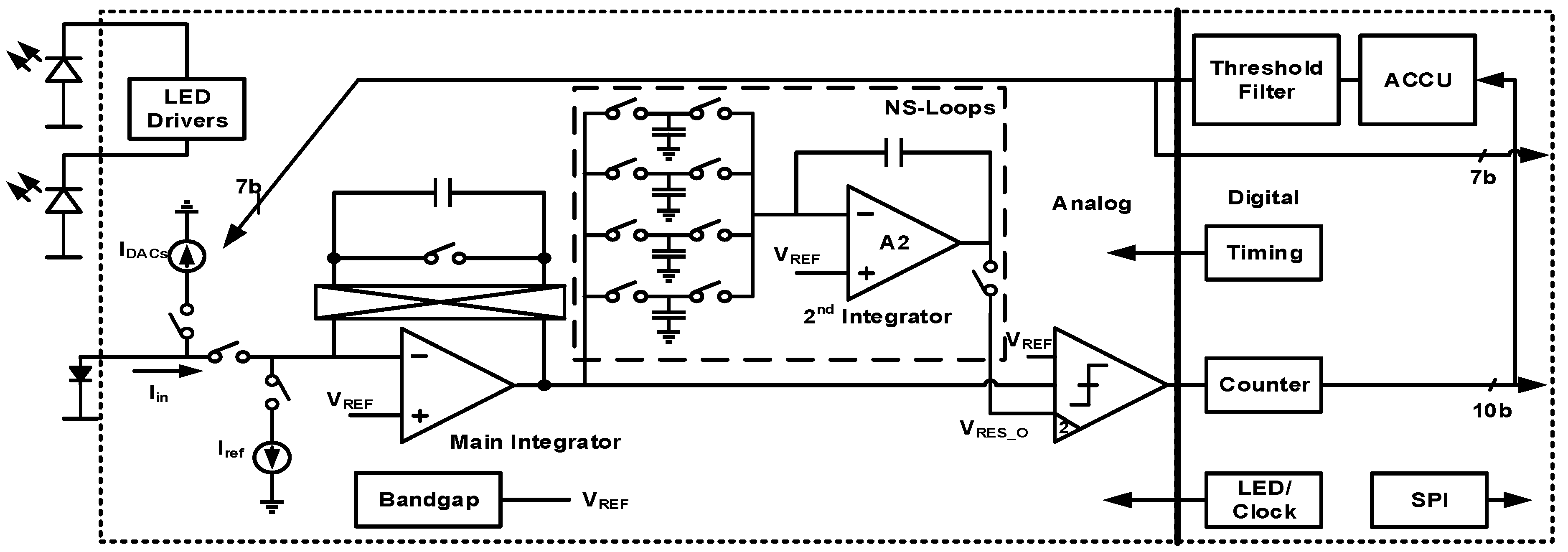
4. Techniques for Bio-Optical Signal Recording

Photoplethysmogram (PPG) and near infrared spectroscopy (NIRS) are optical sensing modes that not only provide heart rate as conventional ECG, but also enable calculation of blood oxygen saturation (SpO2). PPG obtains the pulsating changes in the volume of blood vessels along with the pulsation of the heart by recording the light absorption of the measured part in real time. Similar to biopotential signal recording systems, bio-optical recording systems should also feature low power, low noise and small chip area to reduce costs. What is more, the PPG signal consists of an AC component and a DC component, and the ratio of AC/DC can be as low as 0.1%; therefore, another challenge of the PPG sensor readout system is to achieve a high DR [25,26]. A conventional PPG readout circuits includes a TIA, an anti-aliasing filter, a sample/hold circuit and an ADC. The ADC quantization noise and nonlinearity can limit the PPG sensor DR [27,28,29,30]. Therefore, DDC techniques play an important role in minimizing the power, noise and chip area while providing a high DR [31,32].
In terms of a low-power PPG system, reducing the power of LED drivers is significant. The system feedbacks the PPG output to the LED driver to control the driving current dynamically in [33]. As shown in Figure 14, a TIA followed with a nine-bit ADC is used to convert the PPG input current to a digital signal. Dynamic Range Enhancement (DRE) is implemented, which includes a digital filter to obtain the DC components of the PPG signal. This DC component is feedbacked to subtract the static photocurrents, so the accuracy requirement for Aa is relaxed. Moreover, the digital output value can dynamically adjust the LED driving current to ensure that the driving current is in a reasonable state. In this way, the system achieves a 87 dB time-varying interference attenuation with a 425 μW power consumption. However, the dynamic range is limited by DRE.
Compressive sampling is another technique to save LED driving currents [34]. As shown in Figure 15, the signal is sampled at a sub-Nyquist frequency and adjacent samples are uneven in time distribution. Hence, the LED driving current is proportionally reduced. The feature extraction units, which are included in the digital back end (DBE), analyze the digital signal and determine the systolic peaks of the PPG signals. Then, the system estimates when the next peak will arrive and enable the LED pulse at that time. The system uses a 30× compression ratio and finally reduces the whole power consumption to 172 μW. However, once the PPG signal changes, the system misses the peak information and needs time to recalibrate.
To obtain peak information more comprehensively and faster, a low-power PPG sensor with a heartbeat-locked loop (HBLL) is proposed in [35]. As shown in Figure 16, AFE consists of DC–current cancellation circuits, a transimpedance amplifier (TIA), switched capacitor low-pass filters (SC-LPF), two S/Hs and a comparator. The comparator compares two adjacent PPG samples and outputs PPGCLK signals according to the change in PPG signals. The HBLL receives the PPGCLK signals and estimates the heartbeat interval (HBI) by using a counter. Based on the HBI, the LED pulse and sampling are only enabled during the PPG peak windows precisely. Therefore, the power consumption of the LED driver is reduced from 105 μW to 16 μW with accurate HR monitoring. However, this work can only obtain PPG peak information. In SpO2 monitoring, the whole PPG signal should be recorded.
Apart from reducing the power consumption of LED drivers, optimizing PD is another way to achieve low-power PPG sensors. Integrating the PD on the chip can save area and simplify the system architecture while offering good tradeoffs of power and noise. An integrated monolithic PPG sensor with on-chip pinned photodiodes (PPD) is proposed [36]. PPD is commonly used in CMOS image sensors (CIS) due to their high sensitivity. Therefore, this work achieves the same signal-to-noise (SNR) ratio compared to that of the conventional architecture at a significantly lower power. As shown in Figure 17, averaging is applied to reduce the read noise and relax DR requirements. Then, the PPG signal is adjusted to suitable voltage range by a programmable gain low-power SC amplifier. A 14-bit ADC is used for data conversion. Finally, with a low LED duty cycle, LED only consumes 1.97 μW and AFE consumes 2.63 μW.
Table 3 summarizes the power consumption of state-of-the-art PPG readout circuits. It is worth noticing that various technologies have been implemented to rapidly reduce the LED power and AFE power of a PPG system, even at the cost of area.
As illustrated before, accurate recording of PPG signals requires high DR of the readout system. The majority of the PPG signal is the DC component; therefore, the main ADC power is used to quantify DC currents. A workable solution is the use of a DC servo loop to subtract the DC components before the input signals enter TIA. F. Marefat proposed a new light-to-digital convertor (LDC) which allows the measurements of DC and ambient components of the PD current for signal cancellation [31]. As shown in Figure 18a, two eight-bit IDACs are implemented to compensate the ambient light, as well as DC components, which are recorded for further processing as well. PDACs serve as main-feedback DAC of LDC, and nDACs replicating pDACs relax the current-drive requirements of the amplifier. This topology can achieve a 92.7 dB DR while consuming 8.1 μW power. Based on this concept, a second-order ∆∑ LDC is applied for benefiting from two-stage noise shaping [37]. As shown in Figure 18b, two 10-bit DACs instead of 8-bit DACs are employed to cancellate the ambient light and DC components. Multiple DACs are implemented to complete the closed loop while ensuring linearity. However, the second-order architecture benefits from lower noise, but also consumes higher amounts of power. In this work, a 108.2 dB DR is achieved while using a 15.7 μW AFE power. Since oversampling is necessary for noise shaping, a higher pulse frequency is required with higher LED power.
Q. Lin proposed a reconfigurable LDC for PPG sensor readout in [38] which utilizes a current integration and a charge counting to reduce noise contribution. As shown in Figure 19, this LDC consists of a latched comparator, a current reference, a counter and an integrator. A current DAC is implemented to cancel ambient current to increase DR. Finally, this work achieves a 119 dB DR with a 196 μW power consumption.
Dual-slope ADC is an excellent solution for the required high DR of PPG monitoring. Further, this architecture is also suitable for low-bandwidth and linearity requirements. To reduce AFE power consumption caused by dual-slope ADC long-time conversion, a hybrid-architecture-slope LDC is proposed [39]. With noise shaping, the hybrid architecture quantizer can be lower to achieve the same resolution as that of the pure dual-slope quantizer. As shown in Figure 20, a 10-bit quantizer is used to convert the integrator output to a digital code. An on-chip digital threshold filter controls a seven-bit IDAC to compensate the DC components of PPG signals. This work achieves a 134 dB DR while consuming 28 μW of power.
Table 4 summarizes the comparison of state-of-the-art high-DR PPG readout circuits. In [31], an LDC with an eight-bit IDAC was proposed consisting of pDACs and nDACs. With a 10.24% LED duty cycle, the system achieves 92.7 dB consuming 8.1 uW. Based on [31], in [37], a second-order LDC was proposed. In this work, the circuit benefits from lower noise (DR = 108.2 dB), but consumes a higher amount of power (15.1 μW). However, the systems in both [31] and [37] consume a large amount of LED power (1950 μW and 264 μW). In [38], reconfigurable LDC was proposed which uses a current integrator and a DAC. The model in this work achieves a 119 dB DR with a 196 μW power consumption. Although the power of AFE is high, with lower LED duty cycle (1%), LED power is lower than that of [31,37]. In [39], a hybrid-architecture slope LDC was proposed to reduce AFE power. The system in work achieves a 134 dB DR with only 28 μW of AFE power.
In a bio-optical signal recording system, the LED power consumption is the main contributor to the system power consumption compared to AFE. Compared to using a one-bit quantizer LDC [31,37] structure, using slope-based LDC [38] and dual-slope-based LDC [39] can greatly reduce LED power consumption by low LED pulse frequency. Furthermore, compared to [38], although the dual-slope-based LDC has a higher rate of AFE power consumption, it has higher DR while consuming less LED power.

5. Conclusions

This paper describes an overview of biomedical signal readout circuits. In the ECG monitoring domain, a direct digital conversion technique has been proposed in recent years, which employs preamplifier and data converters, reducing the complexity of the readout chain and thus its power consumption. To be suitable for low power supply and process node, VCO-based architecture is proposed. However, all methods have poor performance in input impedance. Boosting input impedance is still a significant highlight of the biomedical sensor. For bio-optical monitoring, low power consumption and high DR are the main challenges. Determining a way to provide a good tradeoff between DR, AFE power and LED power is the focus of PPG design in the future.

Author Contributions

Conceptualization, Y.Z. and S.S.; methodology, Y.Z., S.W. and M.Z.; validation, Y.Z., S.S. and Y.W.; formal analysis, Y.Z. and X.Y.; investigation, Y.Z., S.S. and T.Y.; writing—original draft preparation, Y.Z.; writing—review and editing, Y.Z., S.S., S.W., Y.W., T.Y., X.Y. and M.Z. All authors have read and agreed to the published version of the manuscript.

Funding

This research is supported by Young Talent Grants of ZJU-HIC under number 04010000-K02013201. It also receives support from Kunpeng Grants of Zhejiang province under number 04010000-K2A033201.

Data Availability Statement

Not applicable.

Conflicts of Interest

The authors declare no conflict of interest.

References

  1. Song, S.; Konijnenburg, M.; Van, W.R.; Xu, J.; Ha, H.; Sijbers, W.; Stanzione, S.; Biswas, D.; Breeschoten, A.; Vis, P.; et al. A 769 μW Battery-Powered Single-Chip SoC with BLE for Multi-Modal Vital Sign Monitoring Health Patches. IEEE Trans. Biomed. Circuits Syst. 2019, 13, 1506–1517. [Google Scholar] [CrossRef] [PubMed]
  2. Van, H.N.; Konijnenburg, M.; Pettine, J.; Jee, D.W.; Kim, H.; Morgado, A.; Van, W.R.; Torfs, T.; Mohan, R.; Breeschoten, A.; et al. A 345 µW Multi-Sensor Biomedical SoC with Bio-Impedance, 3-Channel ECG, Motion Artifact Reduction, and Integrated DSP. IEEE J. Solid-State Circuit 2015, 50, 230–244. [Google Scholar]
  3. Xu, J.; Konijnenburg, M.; Song, S.; Ha, H.; Van, W.R.; Mazzillo, M.; Fallica, G.; Van, H.C.; De, R.W.; Van, H.N. A 665 μW Silicon Photomultiplier-Based NIRS/EEG/EIT Monitoring ASIC for Wearable Functional Brain Imaging. IEEE Trans. Biomed. Circuits Syst. 2018, 12, 1267–1277. [Google Scholar] [CrossRef] [PubMed]
  4. Mora, L.C.; Putzeys, J.; Raducanu, B.C.; Ballini, M.; Wang, S.; Andrei, A.; Rochus, V.; Vandebriel, R.; Severi, S.; Van, H.C.; et al. A Neural Probe with Up to 966 Electrodes and Up to 384 Configurable Channels in 0.13 μm SOI CMOS. IEEE Trans. Biomed. Circuits Syst. 2017, 11, 510–522. [Google Scholar] [CrossRef] [PubMed] [Green Version]
  5. Raducanu, B.; Van, H.C.; Kloosterman, F. Massive Parallel Readout Circuits for In-Vivo Signal Acquisition. In Sterk Geparallelliseerde Uitleesschakelingen Voor In-Vivo Signaalacquisitie; 2018. Available online: https://imec-publications.be/handle/20.500.12860/31591 (accessed on 26 October 2021).
  6. Chandrakumar, H.; Markovic, D. A 2 μW 40 mVpp linear input-range chopper-stabilized bio-signal amplifier with boosted input impedance of 300 MΩ and electrode-offset filtering. In Proceedings of the 2016 IEEE International Solid-State Circuits Conference (ISSCC), San Francisco, CA, USA, 31 January–4 February 2016; pp. 96–97. [Google Scholar]
  7. Kassiri, H.; Pazhouhandeh, R.; Soltani, N.; Salam, M.T.; Carlen, P.; Velazquez, J.L.P.; Genov, R. All-wireless 64-channel 0.013 mm2/ch closed-loop neurostimulator with rail-to-rail DC offset removal. In Proceedings of the 2017 IEEE International Solid-State Circuits Conference (ISSCC), San Francisco, CA, USA, 11–15 February 2017; pp. 452–453. [Google Scholar]
  8. Pazhouhandeh, M.R.; Kassiri, H.; Shoukry, A.; Weisspapir, I.; Carlen, P.L.; Genov, R. Opamp-Less Sub-μW/Channel Δ-Modulated Neural-ADC with Super-GΩ Input Impedance. IEEE J. Solid-State Circuit 2021, 56, 1565–1575. [Google Scholar] [CrossRef]
  9. Yang, X.; Xu, J.; Ballini, M.; Chun, H.; Zhao, M.; Wu, X.; Van, H.C.; Mora, L.C.; Van Helleputte, N. A 108 dB DR Δ∑-∑M Front-End with 720 mVpp Input Range and >±300 mV Offset Removal for Multi-Parameter Biopotential Recording. IEEE Trans. Biomed. Circuits Syst. 2021, 15, 199–209. [Google Scholar] [CrossRef] [PubMed]
  10. Kim, C.; Joshi, S.; Courellis, H.; Wang, J.; Miller, C.; Cauwenberghs, G. Sub μVrms-Noise Sub μW/Channel ADC-Direct Neural Recording with 200-mV/ms Transient Recovery Through Predictive Digital Autoranging. IEEE J. Solid-State Circuit 2018, 53, 3101–3110. [Google Scholar] [CrossRef] [Green Version]
  11. Van Wegberg, R.; Sijbers, W.; Song, S.; Breeschoten, A.; Vis, P.; Konijnenburg, M.; Jiang, H.; Rooijakkers, M.; Berset, T.; Penders, J.; et al. A 5-Channel Unipolar Fetal-ECG Readout IC for Patch-Based Fetal Monitoring. IEEE Solid-State Circ. Lett. 2019, 2, 71–74. [Google Scholar] [CrossRef]
  12. Wang, S.; Ballini, M.; Yang, X.; Sawigun, C.; Weijers, J.W.; Biswas, D.; Van Helleputte, N.; Lopez, C.M. A Compact Chopper Stabilized Δ-ΔΣ Neural Readout IC with Input Impedance Boosting. IEEE Open J. Solid-State Circuits Soc. 2021, 1, 67–78. [Google Scholar] [CrossRef]
  13. Sporer, M.; Reich, S.; Kauffman, J.G.; Ortmanns, M. A Direct Digitizing Chopped Neural Recorder Using a Body-Induced Offset Based DC Servo Loop. IEEE Trans. Biomed. Circuits Syst. 2022, 16, 409–418. [Google Scholar] [CrossRef] [PubMed]
  14. Wendler, D.; Dorigo, D.D.; Amayreh, M.; Bleitner, A.; Marx, M.; Manoli, Y. A 0.00378 mm2 Scalable Neural Recording Front-End for Fully Immersible Neural Probes Based on a Two-Step Incremental Delta-Sigma Converter with Extended Counting and Hardware Reuse. In Proceedings of the 2021 IEEE International Solid-State Circuits Conference (ISSCC), San Francisco, CA, USA, 13–22 February 2021; pp. 398–400.
  15. Jiang, H.; Makinwa, K.A.A.; Nihtianov, S. An energy-efficient 3.7 nV/√Hz bridge-readout IC with a stable bridge offset compensation scheme. In Proceedings of the 2017 IEEE International Solid-State Circuits Conference (ISSCC), San Francisco, CA, USA, 11–15 February 2017; pp. 172–173.
  16. Jiang, H.; Liu, Y.; Middelburg, L.; Mansouri, B.E.; Nihtianov, S. A Continuous-Time Readout IC with 0.12 aF/√Hz for Capacitive Inertial Sensors. In Proceedings of the 2021 IEEE International Conference on Integrated Circuits, Technologies and Applications (ICTA), Zhuhai, China, 24–26 November 2021; pp. 14–15.
  17. Mark, K.L. Deep Brain Stimulation: Current and Future Clinical Applications. Mayo Clin. Proc. 2011, 86, 662–672. [Google Scholar]
  18. Jiang, W.; Hokhikyan, V.; Chandrakumar, H.; Karkare, V.; Markovic, D. A ±50 mV linear-input-range VCO-based neural-recording front-end with digital nonlinearity correction. In Proceedings of the 2016 IEEE International Solid-State Circuits Conference (ISSCC), San Francisco, CA, USA, 31 January–4 February 2016; pp. 484–485. [Google Scholar]
  19. Li, S.; Zhao, W.; Xu, B.; Yang, X.; Tang, X.; Shen, L.; Lu, N.; Pan, D.Z.; Sun, N. A 0.025-mm2 0.8-V 78.5 dB-SNDR VCO-Based Sensor Readout Circuit in a Hybrid PLL-ΔΣM Structure. In Proceedings of the 2019 IEEE Custom Integrated Circuits Conference (CICC), Austin, TX, USA, 14–17 April 2019; pp. 1–3.
  20. Huang, J.; Mercier, P.P. A 112-dB SFDR 89-dB SNDR VCO-Based Sensor Front-End Enabled by Background-Calibrated Differential Pulse Code Modulation. IEEE J. Solid-State Circuit 2021, 56, 1046–1057. [Google Scholar] [CrossRef]
  21. Pochet, C.; Hall, D.A. A 4.4 μW 2.5 kHz-BW 92.1 dB-SNDR 3rd-Order VCO-Based ADC with Pseudo Virtual Ground Feedforward Linearization. In Proceedings of the 2022 IEEE International Solid-State Circuits Conference (ISSCC), San Francisco, CA, USA, 20–26 February 2022; pp. 408–410.
  22. Lee, C.; Jeon, T.; Jang, M.; Park, S.; Kim, J.; Lim, J.; Ahn, J.H.; Huh, Y.; Chae, Y. A 6.5-μW 10-kHz BW 80.4-dB SNDR Gm-C-Based CT ∆∑ Modulator with a Feedback-Assisted Gm Linearization for Artifact-Tolerant Neural Recording. IEEE J. Solid-State Circuit 2020, 55, 2889–2901. [Google Scholar] [CrossRef]
  23. Huang, X.; Zeng, K.; Liu, Y.; Rhee, W.; Kim, T.; Wang, Z. A 5GHz 200kHz/5000ppm Spread-Spectrum Clock Generator with Calibration-Free Two-Point Modulation Using a Nested-Loop BBPLL. In Proceedings of the 2019 IEEE Custom Integrated Circuits Conference (CICC), Austin, TX, USA, 14–17 April 2019; pp. 1–4. [Google Scholar]
  24. Huang, X.; Wang, B.; Rhee, W.; Wang, Z. A 5.4GHz ΔΣ Bang-Bang PLL with 19dB In-Band Noise Reduction by Using a Nested PLL Filter. In Proceedings of the 2020 International Symposium on VLSI Design, Automation and Test (VLSI-DAT), Hsinchu, Taiwan, 10–13 August 2020; pp. 1–2.
  25. Antonino, C. An Ultra Low-Noise Micropower PPG Sensor; EPFL: Lausanne, Switzerland, 2020. [Google Scholar]
  26. Glaros, K.N.; Drakakis, E.M. A Sub-mW Fully-Integrated Pulse Oximeter Front-End. IEEE Trans. Biomed. Circuits Syst. 2013, 7, 363–375. [Google Scholar] [CrossRef] [PubMed]
  27. Sharma, A.; Bae, L.S.; Polley, A.; Narayanan, S.; Li, W.; Sculley, T.; Ramaswamy, S. Multi-modal smart bio-sensing SoC platform with >80 dB SNR 35 µA PPG RX chain. In Proceedings of the 2016 IEEE Symposium on VLSI Circuits (VLSI-Circuits), Honolulu, HI, USA, 15–17 June 2016; pp. 1–2. [Google Scholar]
  28. Schönle, P.; Fateh, S.; Burger, T.; Huang, Q. A power-efficient multi-channel PPG ASIC with 112 dB receiver DR for pulse oximetry and NIRS. In Proceedings of the 2017 IEEE Custom Integrated Circuits Conference (CICC), Austin, TX, USA, 30 April–3 May 2017; pp. 1–4. [Google Scholar]
  29. Harpe, P.; Cantatore, E.; Van Roermund, A. An oversampled 12/14b SAR ADC with noise reduction and linearity enhancements achieving up to 79.1dB SNDR. In Proceedings of the 2014 IEEE International Solid-State Circuits Conference Digest of Technical Papers (ISSCC), San Francisco, CA, USA, 9–13 February 2014; pp. 194–195. [Google Scholar]
  30. Atef, M.; Wang, M.; Wang, G. A Fully Integrated High-Sensitivity Wide Dynamic Range PPG Sensor with an Integrated Photodiode and an Automatic Dimming Control LED Driver. IEEE Sens. J. 2018, 18, 652–659. [Google Scholar] [CrossRef]
  31. Marefat, F.; Erfani, R.; Mohseni, P. A 1-V 8.1-μW W PPG-Recording Front-End with > 92-dB DR Using Light-to-Digital Conversion with Signal-Aware DC Subtraction and Ambient Light Removal. IEEE Solid-State Circ. Lett. 2020, 3, 17–20. [Google Scholar] [CrossRef]
  32. Alhawari, M.; Albelooshi, N.A.; Perrott, M.H. A 0.5 V < 4 μW CMOS Light-to-Digital Converter Based on a Nonuni-form Quantizer for a Photoplethysmographic Heart-Rate Sensor. IEEE J. Solid-State Circuit 2014, 49, 271–288. [Google Scholar]
  33. Winokur, E.S.; O’dwyer, T.; Sodini, C.G. A Low-Power, Dual-Wavelength Photoplethysmogram (PPG) SoC with Static and Time-Varying Interferer Removal. IEEE Trans. Biomed. Circuits Syst. 2015, 9, 581–589. [Google Scholar] [CrossRef] [PubMed]
  34. Rajesh, P.V.; Valero-Sarmiento, J.M.; Yan, L.; Bozkurt, A.; Van Hoof, C.; Van Helleputte, N.; Yazicioglu, R.F.; Verhelst, M. A 172 µW compressive sampling photoplethysmographic readout with embedded direct heart-rate and variability extraction from compressively sampled data. In Proceedings of the 2016 IEEE International Solid-State Circuits Conference (ISSCC), San Francisco, CA, USA, 31 January–4 February 2016; pp. 386–387. [Google Scholar]
  35. Jang, D.H.; Cho, S. A 43.4 μW photoplethysmogram-based heart-rate sensor using heart-beat-locked loop. In Proceedings of the 2018 IEEE International Solid-State Circuits Conference (ISSCC), San Francisco, CA, USA, 11–15 February 2018; pp. 474–476.
  36. Caizzone, A.; Boukhayma, A.; Enz, C. A 2.6 μW Monolithic CMOS Photoplethysmographic Sensor Operating with 2 μW LED Power. In Proceedings of the 2019 IEEE International Solid-State Circuits Conference (ISSCC), San Francisco, CA, USA, 17–21 February 2019; pp. 290–291.
  37. Marefat, F.; Erfani, R.; Kilgore, K.L.; Mohseni, P. A 280 µW 108 dB DR Readout IC with Wireless Capacitive Powering Using a Dual-Output Regulating Rectifier for Implantable PPG Recording. In Proceedings of the 2020 IEEE International Solid-State Circuits Conference (ISSCC), San Francisco, CA, USA, 16–20 February 2020; pp. 412–414. [Google Scholar]
  38. Lin, Q.; Xu, J.; Song, S.; Breeschoten, A.; Konijnenburg, M.; Van Hoof, C.; Tavernier, F.; Van Helleputte, N. A 119 dB Dynamic Range Charge Counting Light-to-Digital Converter For Wearable PPG/NIRS Monitoring Applications. IEEE Trans. Biomed. Circuits Syst. 2020, 14, 800–810. [Google Scholar] [CrossRef] [PubMed]
  39. Lin, Q.; Song, S.; Wegberg, R.V.; Konijnenburg, M.; Biswas, D.; Hoof, C.V.; Tavernier, F.; Helleputte, N.V. A 28 μW 134 dB DR 2nd-Order Noise-Shaping Slope Light-to-Digital Converter for Chest PPG Monitoring. In Proceedings of the 2021 IEEE International Solid-State Circuits Conference (ISSCC), San Francisco, CA, USA, 13–22 February 2021; pp. 390–392. [Google Scholar]
Figure 1. (a) Conventional AC-coupled neural amplifiers; (b) digitally assisted DC-coupled neural amplifiers.
Electronics 12 02676 g001
Figure 2. Pseudo-resistor realized by current bias.
Electronics 12 02676 g002
Figure 3. (a) Classical first-order ∆∑-based ADC; (b) first-order ∆2∑-based ADC.
Electronics 12 02676 g003
Figure 4. Block diagram of ∆-modulator.
Electronics 12 02676 g004
Figure 5. Block diagram of ∆∑-∑modulator.
Electronics 12 02676 g005
Figure 6. Block diagram of ∆-∆∑modulator.
Electronics 12 02676 g006
Figure 7. (a) A discrete-time integrator; (b) A continuous-time integrator Gm stage.
Electronics 12 02676 g007
Figure 8. Gm-C-based ∆-∆∑ modulator.
Electronics 12 02676 g008
Figure 9. Block of VCO-based modulator.
Electronics 12 02676 g009
Figure 10. (a) The conceptual diagram of the proposed PLL-ΔΣM system; (b) schematic of Gm stage.
Electronics 12 02676 g010
Figure 11. The diagram of the VCO-based system with DPCM.
Electronics 12 02676 g011
Figure 12. The diagram of the 3rd-order VCO-based system with pseudo-virtual ground.
Electronics 12 02676 g012
Figure 13. The diagram of Gm-C-based CTDSM.
Electronics 12 02676 g013
Figure 14. The static and time-varying interferer removal PPG system.
Electronics 12 02676 g014
Figure 15. The diagram of compressive-sampling (CS)-based PPG system.
Electronics 12 02676 g015
Figure 16. The AFE and LED driver schematic of HBLL.
Electronics 12 02676 g016
Figure 17. Architecture of the monolithic PPG sensor.
Electronics 12 02676 g017
Figure 18. (a) Block diagram of I-∆∑ LDC; (b) second-order I-∆∑ LDC.
Electronics 12 02676 g018
Figure 19. Block diagram of the LDC.
Electronics 12 02676 g019
Figure 20. Architecture of NS LDC.
Electronics 12 02676 g020
Table 1. Performance of state-of-the-art DDC biopotential readout circuits.
[7][9][10][8][12][13][14]
Technology (nm)1301806513055180180
Supply (V)1.2/2.51.80.80.6/1.2/3.31.21.81.8
Architecture2∆∑2222nd order ∆∑Gm-C I-∆∑
NO. of channel64-161616168–24
Zin (MΩ)<10034>262960663238-
Input range (mVpp)-720260-1481914
Input noise (µVrms)1.130.980.982.65.53 15.55 13.93 1
Bandwidth (kHz)0.50.10.50.5101010
EDO tolerance (mV)±1200>±300±130±1500±70±100±100
SNDR (dB)72.266.2666059.561.157.5
Power/channel (μW)0.6373.80.80.9961.212.814.94
Area/channel (mm2)5.980.480.0240.0110.00770.020.0046
1 Input noise at frequency of AP.
Table 2. Performance of state-of-the-art VCO-based DDC biopotential readout circuits.
[18][19][22][20][21]
Technology (nm)13040556565
Supply (V)1.2A/0.45D 10.8A/0.6D 111.2A/0.7D 10.8
Fs (Hz)5 K2.5 M1.28 M32 K400 K
Zin (MΩ)20.2213.3 34-
Input range (mVpp)501003002501800
Input noise (nV/√Hz)95369553
Bandwidth (kHz)0.210100.52.5
SNDR (dB)7678.580.489.292.1
CMRR (dB)6683769880–93
Power (μW)74.56.53.24.4
Area (mm2)0.1350.0250.0780.080.1
FOM 4 (dB)150.5172172.3171.2179.6
1 A represents analog-domain; D represents digital-domain. 2 Theoretical calculated value. 3 At 10 KHz. 4 FOM = P/(2ENOB*Fs).
Table 3. Performance of state-of-the-art PPG readout circuits.
[33][34][35][36]
Technology (nm)180180180180
Supply (V)1.81.23.31.8A/3.3D 1
Pulse Frequency (Hz)1654–12840–10040
LED Duty cycle0.7%-0.0175–1.75%0.07%
LED Power (μW)120–112543–120016–5201.97 2
AFE Power (μW)21617227.42.63
Area (mm2)1.84101.5120
1 A represents analog domain; D represents digital domain. 2 Green LED = 12.04 μW; red LED = 1.97 μW.
Table 4. Comparison of state-of-the-art high DR bio-optical readout circuits.
[31][37][38][39]
Technology (nm)180180180180
Supply (V)1A/2.5D 11.5A/2.5D 11.2/3.3 11.2A/3.3D 1
Amb. Remove (μA)28.225.6 25050
ArchitectureLDC
(ISDM)
LDC
(ISDM)
LDC
(Slope)
LDC
(NS-Slope)
Input range (μA)51.251.2200200
Pulse Frequency (Hz)1002505122048
Noise BW0.5–100.5–10-0.5–20
DR (dB)92.7108.2119134
LED Duty cycle10.24% 33.2%1%1%
LED Power (μW)1950264107305
AFE Power (μW)8.115.78928
Area (mm2)4.8-7 48.4
1 A represents analog domain; D represents digital domain. 2 10-bit ambient light removal. 3 Needs two LEDs. 4 External cap for filtering reference current.
Disclaimer/Publisher’s Note: The statements, opinions and data contained in all publications are solely those of the individual author(s) and contributor(s) and not of MDPI and/or the editor(s). MDPI and/or the editor(s) disclaim responsibility for any injury to people or property resulting from any ideas, methods, instructions or products referred to in the content.

