Article

A Fast Homeostatic Inhibitory Plasticity Rule Circuit with a Memristive Synapse

1
National Key Laboratory on Electromagnetic Environment Effects, Shijiazhuang Campus, Army Engineering University, Shijiazhuang 050003, China
2
School of Information Science and Engineering, Hebei University of Science and Technology, Shijiazhuang 050018, China
*
Authors to whom correspondence should be addressed.
Electronics 2023, 12(3), 490; https://doi.org/10.3390/electronics12030490
Submission received: 20 December 2022 / Revised: 11 January 2023 / Accepted: 15 January 2023 / Published: 17 January 2023
(This article belongs to the Special Issue Advanced Analog Circuits for Emerging Applications)

Abstract

:
Learning from the robust mechanism of the biological nervous system is critical for creating reliable neuromorphic hardware. The homeostatic inhibition plasticity rule is a robust biological mechanism to balance Hebbian plasticity and resist external environmental disturbances and local damage. It plays an essential role in maintaining the homeostatic sparse firing patterns of the nervous system. This paper imitates this mechanism and provides a fast homeostatic inhibitory plasticity rule circuit with a memristive synapse. Firstly, the design method and principle of the circuit are demonstrated. Secondly, the function of the circuit was verified in PSpice© using a commercial Knowm memristor as a synapse. The PSpice© simulation results show that the circuit can achieve a weight update curve similar to the biological homeostatic inhibitory plasticity rule, and the time scale of the circuit is improved by a factor of 1000 compared to that of the biological nervous system. Furthermore, the circuit has wide applicability due to the tunable qualities of the homeostatic learning window, scaling factor, and homeostatic factor. This study provides new opportunities for building fast and reliable neuromorphic hardware.

1. Introduction

Neuromorphic hardware is a promising intelligent hardware in next-generation information and communication technologies [1,2]. In particular, memristor-based neuromorphic hardware imitates the event-driven characteristics of biological neural networks and the paradigm of processing in memory, which not only greatly reduces hardware power consumption but also improves the real-time performance of information processing [3,4]. Therefore, it distinguishes itself from traditional artificial intelligence hardware and has become a popular research field. However, the application of neuromorphic hardware always faces reliability issues [5,6], and it is necessary to take more action on its reliability design.
To support computation, biological neurons must modulate within an acceptable dynamic range; always-active or never-active neurons convey no information [7,8] and even cause pathological states such as neurological dysfunction and cell death in the nervous system [8,9]. In order to achieve this goal, the biological brain always manages to compensate for changes in neuron activity caused by internal and external disturbances, thereby ensuring the robustness of the nervous system function. A large amount of theoretical and experimental evidence [10,11] demonstrates that homeostatic inhibitory plasticity is one of the crucial mechanisms to promote the robustness of neuronal function. This mechanism can balance Hebbian plasticity and resist external environmental disturbances and local injury by regulating inhibitory synapses to maintain sparse homeostatic fire neuronal activity [12,13,14]. Consequently, this paper draws on the biological presynaptic homeostatic inhibitory plasticity mechanism to construct a synaptic weight learning circuit and provides a new opportunity for designing reliable neuromorphic hardware.
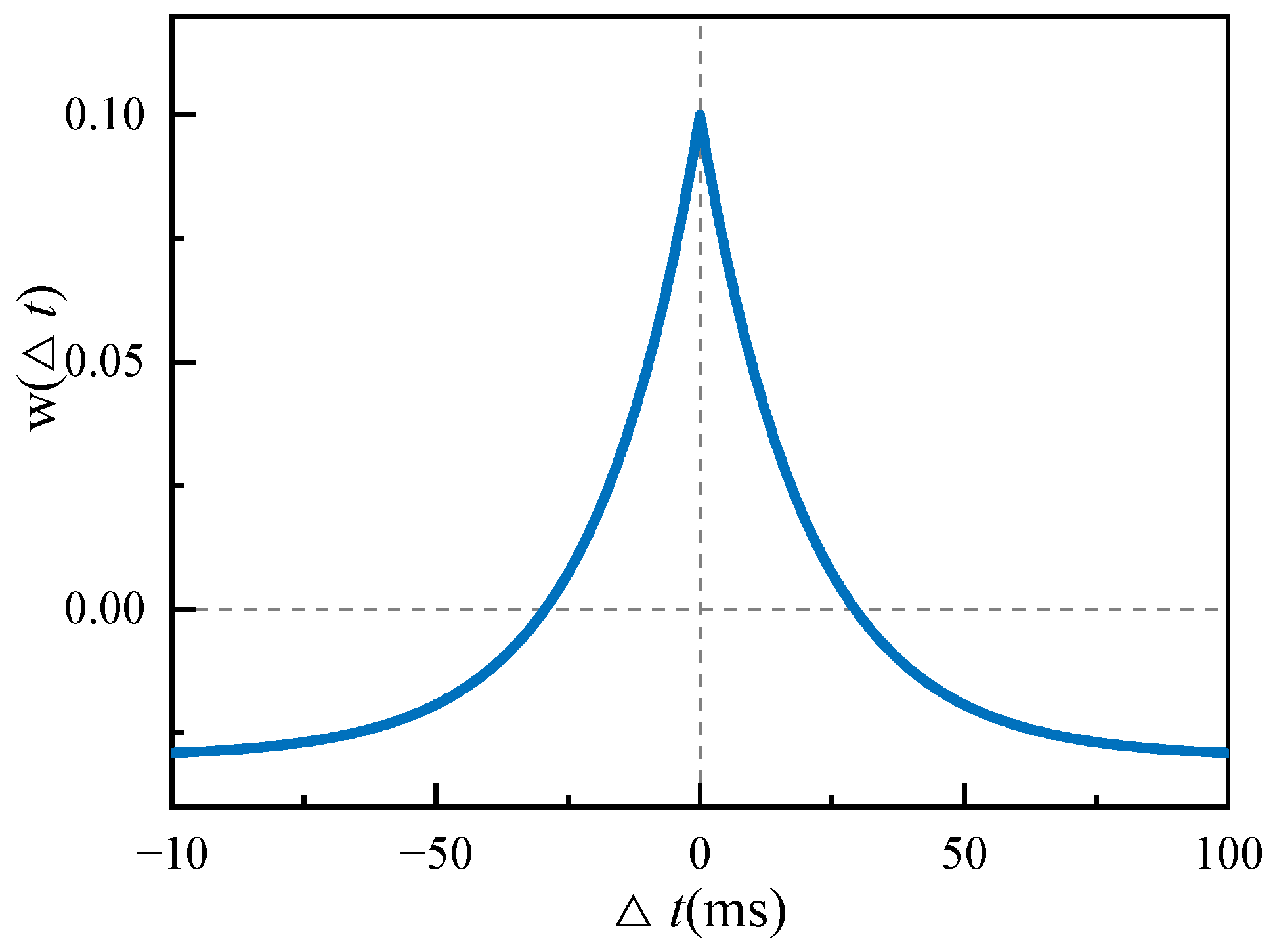
Homeostatic inhibitory plasticity is a spike-timing-dependent plasticity (STDP) mechanism. The mechanism describes an inhibitory synaptic weight change rule: the synaptic weight change w ( Δ t ) decreases with an increase in |∆t| and finally stabilizes to a negative value, as shown in Figure 1. ∆t = tpre tpost is the relative time interval of the pre- and postsynaptic spikes.
The homeostatic inhibition plasticity rule can be expressed as follows:
w ( Δ t ) = { A + e | Δ t | / τ + + w 0 | Δ t | t w A e | Δ t | / τ α | Δ t | > t w
where A+ and A refer to the maximum learning rate; τ + and τ refer to the time constant; w 0 0 is the minimum value of inhibitory synaptic enhancement, w 0 = 0 in Figure 1; and α is the homeostatic factor, which determines the homeostatic firing rate of postsynaptic neurons.
In recent years, many studies have been devoted to implementing STDP rule circuits based on memristive synapses. Methods of implementation are typically classified into two categories. The first category implements the STDP mechanism using a single memristive synapse device [15,16,17]. This STDP rule implementation largely depends on the threshold characteristics of the memristor and the shape of the neural action potential waveform. Although this implementation is structurally simple, its adjustment accuracy is low. It must work with extremely precise neuronal circuits that output the proper shape and consistency of neural action potential waveforms. However, designing such a neuronal circuit is not an easy task. The second category accomplishes the STDP mechanism by combining a memristive synapse and an STDP control circuit [18,19,20]. This STDP implementation mainly relies on the STDP control circuit to generate a square wave signal with different pulse widths that modulates the memristive synaptic conductance. Since the pulse width of the square wave signal is precisely adjustable, this implementation approach may achieve accurate adjustment of the memristive synaptic conductance and has also become a popular method for implementing the STDP rules. Related papers [19,20] using the second method have achieved the antisymmetric Hebbian learning rule, the antisymmetric anti-Hebbian learning rule, the symmetric Hebbian learning rule, and the symmetric anti-Hebbian learning rule. However, to the best of our knowledge, no circuits that implement the homeostatic inhibitory plasticity rule have been reported in currently published papers.
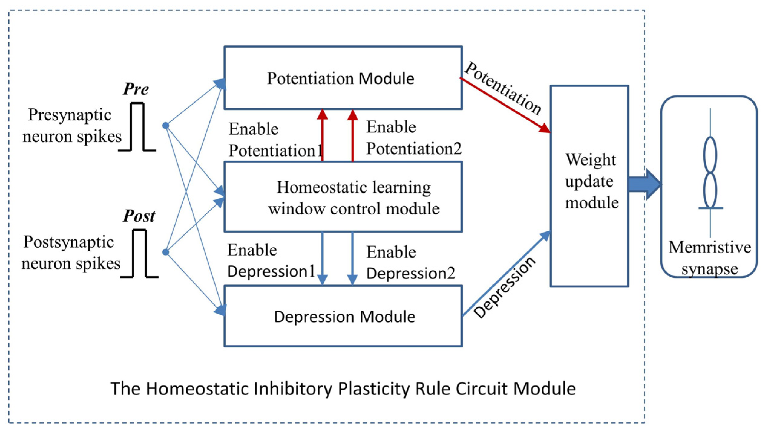
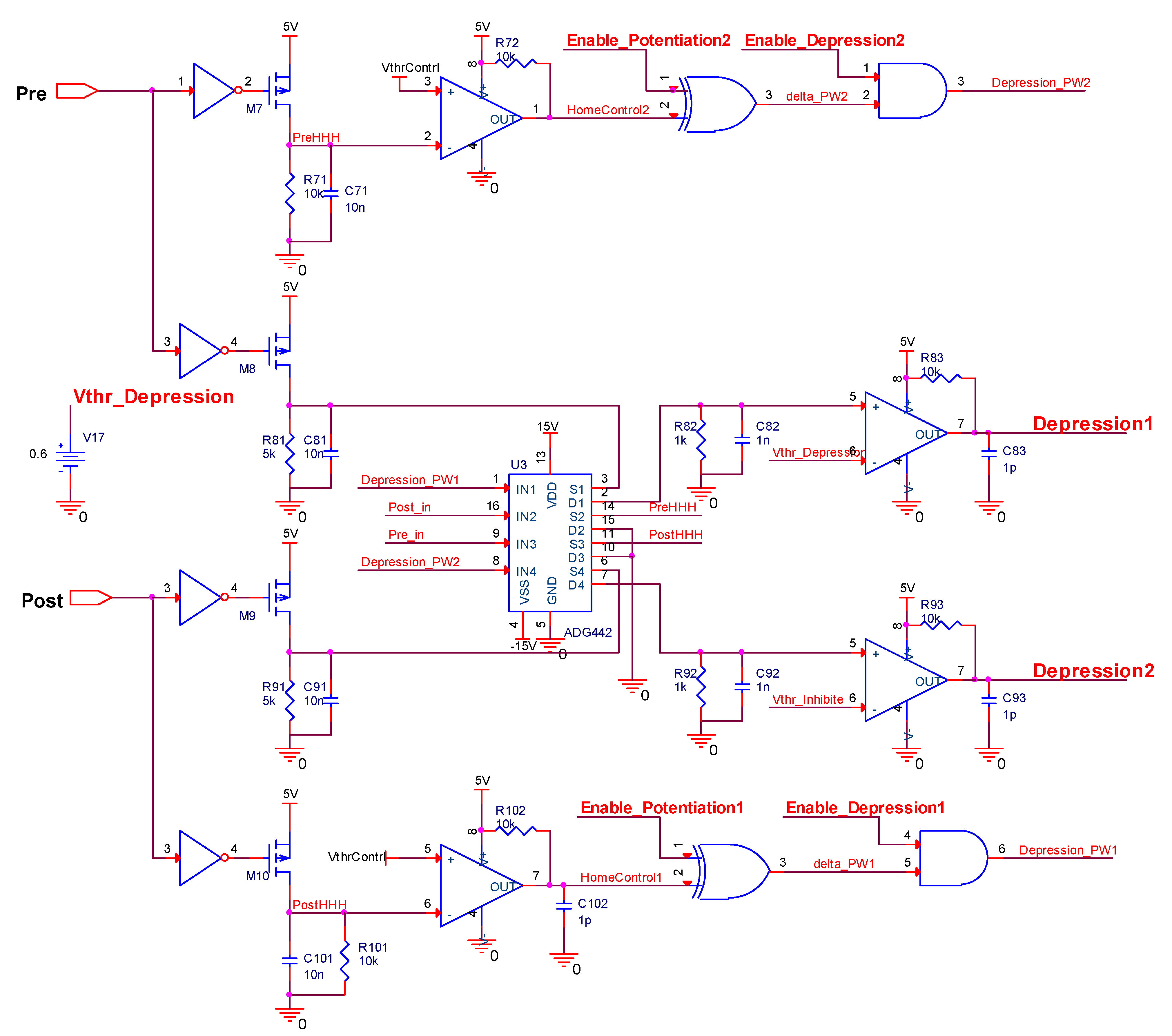
In this research, a homeostatic inhibitory plasticity rule circuit with a memristive synapse is built based on the second STDP implementation approach and the pulse width and amplitude modulation characteristics of memristive conductance, and its performance is verified in PSpice©. The remainder of this paper is organized as follows: The memristor model applied to the synaptic device is introduced in Section 2. Section 3 describes the implementation procedures for the homeostatic inhibitory plasticity circuit. Section 4 analyzes and discusses the PSpice© simulation results of the proposed system. The last Section 5 provides the conclusions.

2. The Memristor Model Used in Synaptic Device

The Knowm self-directed channel (SDC) memristor was the first commercially available memristor fabricated by Knowm Inc. [21,22]. Its material stack is a metal ion-conducting device, which relies on Ag+ movement into channels within the active layer to change the device’s resistance. Therefore, the electrical performance of the Knowm memristor is more stable than that of conventional metal oxide memristors [23]. As a result, it was selected as a potential candidate for the synaptic device. The mathematical model of the Knowm memristor can be represented by Equations (2)–(4).
d x d t = 1 τ ( 1 1 + e β ( v V O N ) ( 1 x ) ( 1 1 1 + e β ( v + V O F F ) ) x )
G m ( x ) = x R O N + 1 x R O F F
i = G m ( x ) v
where x is the state variable of the memristor; VON and VOFF are the thresholds of the memristor ON state and OFF state, respectively; β is the temperature parameter; τ is the time constant of the memristor; Gm is the conductance of the memristor; and i and v are the current and voltage through the memristor, respectively. According to our previous research [24], the i-v characteristics of the Knowm memristor can be better simulated when the parameters are set to the following values: RON = 5.88 kΩ, ROFF = 44.02 KΩ, VON = 0.37 V, VOFF = 0.17 V, and β = 38.46.
As illustrated in Figure 2, the PSpice© model is based on the mathematical model of the Knowm memristor. In Figure 2a, an extra floating XSV pin was added to the model symbol to facilitate its monitoring of the conductance change in the memristor. The voltage at the XSV pin represents the memristor state variable x.
The full listing of the PSpice© model of the Knowm memristor is shown in Appendix A.

3. The Homeostatic Inhibitory Plasticity Rule Circuit

The proposed homeostatic inhibitory plasticity rule circuit is composed of a homeostatic learning window control module, a potentiation module, a depression module, and a weight update module, as shown in the dashed box in Figure 3. Pre and Post represent the square wave pulses generated at the pre- and postsynaptic neuron firing moments, respectively. The homeostatic learning window control module is responsible for generating the enable signal that constrains the homeostatic learning window. The potentiation and depression modules create square wave signals with different pulses to increase and decrease memristive synaptic conductance. The weight update module provides stimulus signals with varying voltage amplitudes to both ends of the memristive synapse based on the pulse width of the potentiation and depression signals, hence modulating the conductance of the memristive synapse. In the following subsections, the detailed circuit implementation of each module will be introduced.

3.1. Homeostatic Learning Window Control Module

The homeostatic learning window control module circuit consists of two parts that represent, respectively, the situation after the arrival of Pre and Post. Figure 4 depicts only the homeostatic learning control circuit after the arrival of Pre, as both parts share the same implementation principle.
The circuit operates as follows when the homeostatic learning window is set to 20 µs and the overall learning window is set to 40 µs. When Pre arrives, transistors M3 and M4 turn on, and capacitors C31 and C41 begin charging. Next, when there is no Pre input, C31 and C41 begin discharging, and M3 and M4 turn off. The following comparator circuits generate a delta 40 µs signal with a 40 µs pulse width and an Enable_Potentiation1 signal with a 20 µs pulse width. Enable_Potentiation1 then conducts an XOR operation with delta 40 µs and outputs Enable_Depression1, allowing the depression module to function. Figure 5 displays the waveforms of Enable_Potentiation1 and Enable_Depression1. The two signals jointly constrain the homeostatic learning window. Using the Pre arrival time as a baseline, if the Post arrives within 20 µs, the potentiation module will start to work, and the synaptic conductance will increase; if the Post arrives after 20 µs, the synaptic depression module will begin to function, and the synaptic conductance will decrease. It is obvious that the homeostatic learning window can be changed by adjusting the voltage values of Vthr40 us and Vthr20 us.

3.2. Potentiation Module

Figure 6 depicts the circuit schematic of the potentiation module. This module circuit was inspired by [19], except that it comprises two identical potentiation signal-generating circuits. The module begins operating when the enable signals Enable_Potentiation1 and Enable_Potentiation2 are at a high level. Pre_enable and Post_enable are signals for starting the two potentiation branches, respectively, and their initial values are both 0 V. When Pre arrives earlier than Post, transistor M1 is activated, capacitor C1 is rapidly charged, Post_enable obtains a high value, and the depression module stops operation. When there is no Pre input, M1 is turned off, and capacitor C1 is discharged through R1. The first switch of the four-way analog switch U1 is activated when the Post arrives. Since C2 is smaller than C1, C1 will charge C2. When the voltage across C2 exceeds Vthr, Potentiation1 outputs a high level. The first switch of U1 is switched off until the Post function ends, and C2 is discharged through R2 until the voltage across it is less than Vthr, at which time Potentiation1 outputs a low level.
According to the working principle of the potentiation module, the pulse width (PW) of the potentiation signals can be controlled by the value of Vthr. Figure 7 depicts the curves of the PW of Potentiation1 and Potentiation2 changing with ∆t under different Vthr, where the range of ∆t is (−40,40) µs, and the simulation step is 1 µs. Since the two potentiation circuit branches are the same, all PW curves are symmetrical about the ∆t = 0 line, and the left and right parts correspond to the PW changes in Potentiation1 and Potentiation2, respectively. Within a particular time window, the PW of the potentiation signals Potentiation1 and Potentiation2 are inversely proportional to ∆t. When Vthr increases, the maximum PW will decrease and the minimum PW will go toward 0. When Vthr = 1.2 V, for instance, the highest PW is only 7.24 µs, and the minimum PW is 0.

3.3. Depression Module

Figure 8 illustrates the circuit schematic of the depression module. The circuit includes two depression signal (Depression1 and Depression2) generation circuits that work on the same principle, corresponding to the arrival of Pre and Post, respectively. Figure 9 shows the time-domain waveforms of several significant node voltages inside the Depression2 generating circuit. When Pre arrives first, transistor M7 turns on, and capacitor C71 begins to charge; once Pre ends, M7 is switched off and C71 begins to discharge slowly. When Post arrives, the second switch of analog switch U3 opens, which grounds the positive terminal of C71 and causes C71 to discharge rapidly, allowing PreHHH to generate a positive pulse. Then, the comparator circuit flips the PreHHH signal and outputs HomeControl2. HomeControl2 and Enable_Potentiation2 perform the XOR operation and then ANDed with Enable_Depression2, forming the control signal Depression_PW2, which regulates the pulse width of Depression2. When Depression_PW2 is at a high level, the fourth switch of U3 is turned on, and C91 rapidly charges C92. When the Post function ends, C92 starts to discharge, and Depression2 outputs a high level until the voltage of C92 is less than Vthr_Inhibite.
The operating principle of the depression module circuit reveals that Vthr regulates the PW of the signals Depression1 and Depression2. Figure 10 illustrates the PW of two depression signals under different Vthr_Depression. The left and right graphs of the dashed line at x = 0 represent the PW changes in Depression1 and Depression2, respectively. In Figure 10, the simulation results demonstrate that when | Δ t | > 20 μ s , the PW of depression pulses increases with | Δ t | and finally stabilizes to a specific value. Moreover, as Vthr_Depression increases, the maximum PW of the depression signals decreases.

3.4. Weight Update Module

Figure 11 illustrates the circuit schematic of the weight update module. The module contains two ADG442 analog switches, which control the pulse direction and amplitude input to the memristive synapse. Mem+ is connected to the top electrode TE of the memristor, and Mem− is connected to the bottom electrode BE of the memristor. When the potentiation signals Potentiation1 or Potentiation2 are inputted, the 2 V voltage stimulus is inputted to the memristor TE according to the width of the potentiation signal, and BE is grounded. When the depression signals Depression1 or Depression2 are inputted, the 0.13 V voltage stimulus is inputted to the memristor BE according to the width of the depression signal, and TE is grounded.

4. PSpice© Simulation Results and Discussion

This section presents the PSpice© simulation results of the homeostatic inhibitory plasticity rule circuit with a Knowm memristive synapse. First, the functionality of the proposed circuit is verified by traversing the Δt and applying continuous pre- and postsynaptic pulses. Second, the PSpice© simulation results are discussed.

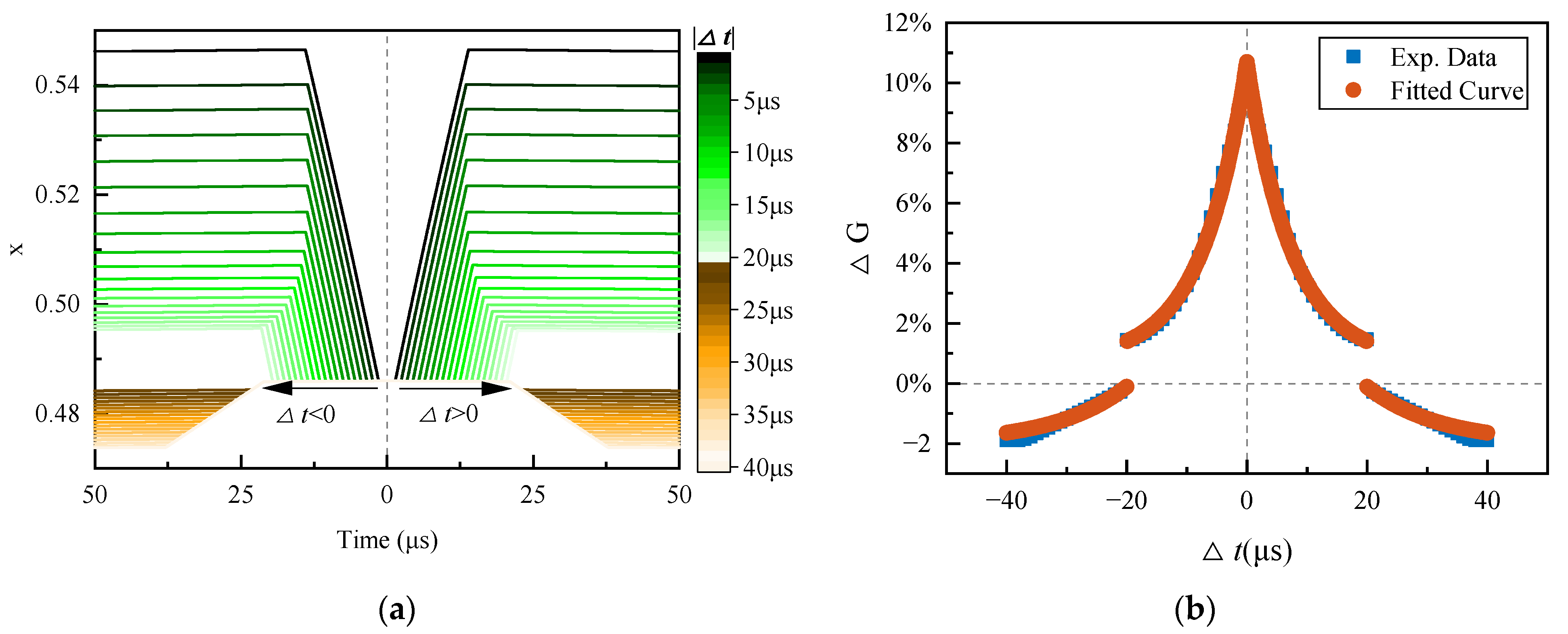
4.1. Traversing the Δt

Set Vthr = 0.5 V and Vthr_Depression = 0.6 V. The traversal range of ∆t is (−40, 40) µs, and the traversal step of ∆t is 1 µs. Since negative parameters cannot be simulated in PSpice©, the situations of ∆t < 0 and ∆t > 0 are simulated separately with a 50 µs simulation time. The waveform of the state variable x of the memristor is obtained, as illustrated in Figure 12a, by monitoring the voltage at the XSV pin of the memristor V(XSV), since V(XSV) represents the memristor state variable x. The plot to the left of the dotted line at Time = 0 is the change in x when ∆t > 0, while the plot to the right represents the change in x when ∆t <0. When |∆t| ≤ 20 µs, x increases, and as |∆t| decreases, x increases more; when |∆t| > 20 µs, x decreases, and as |∆t| increases, x decreases more, and then remains constant.
The conductance of the memristor at any time can be calculated from the relationship between the state variable and the conductance (Equation (3)). Assuming G0 is the initial conductance of the memristor, and G is the updated conductance, the change in the memristive synapse conductance (i.e., the change in synaptic weight) can be calculated as follows:
Δ G = G G 0 G 0 × 100 %
As shown in Figure 12b, the blue symbols represent the change in memristive synaptic conductance with ∆t. Using the biological homeostatic inhibition plasticity learning rule (Equation (1)) to fit the PSpice© experimental data, it is determined that when A+ = A = 0.1, τ + = 7.5 µs, τ - = 12 µs, w 0 = 0.007 , and α = 0.02, Equation (1) can fit the PSpice© experimental data well (shown in orange symbols in Figure 12b). It is indicated that the circuit achieves a homeostatic inhibitory plasticity learning rule similar to a biological one.

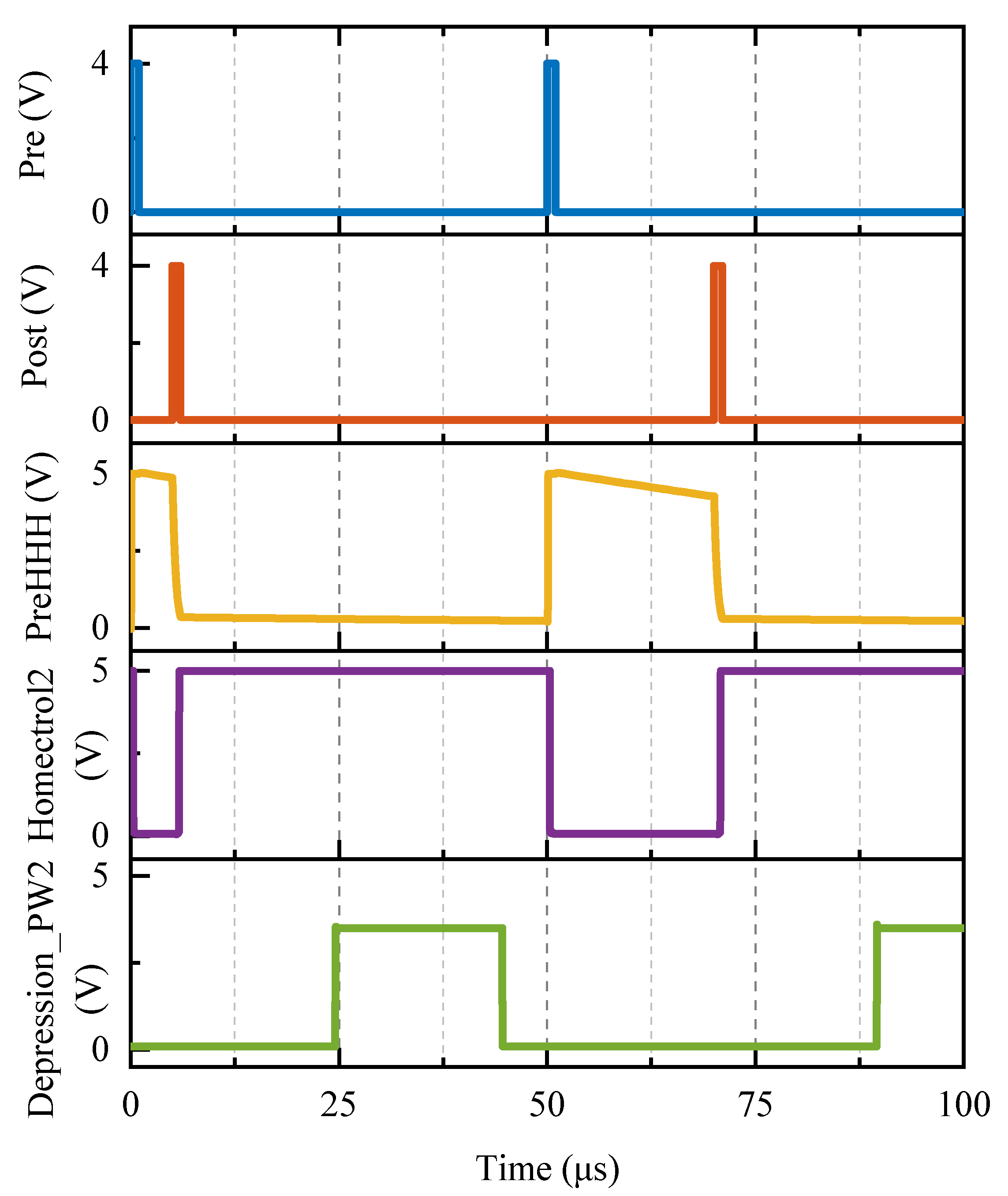
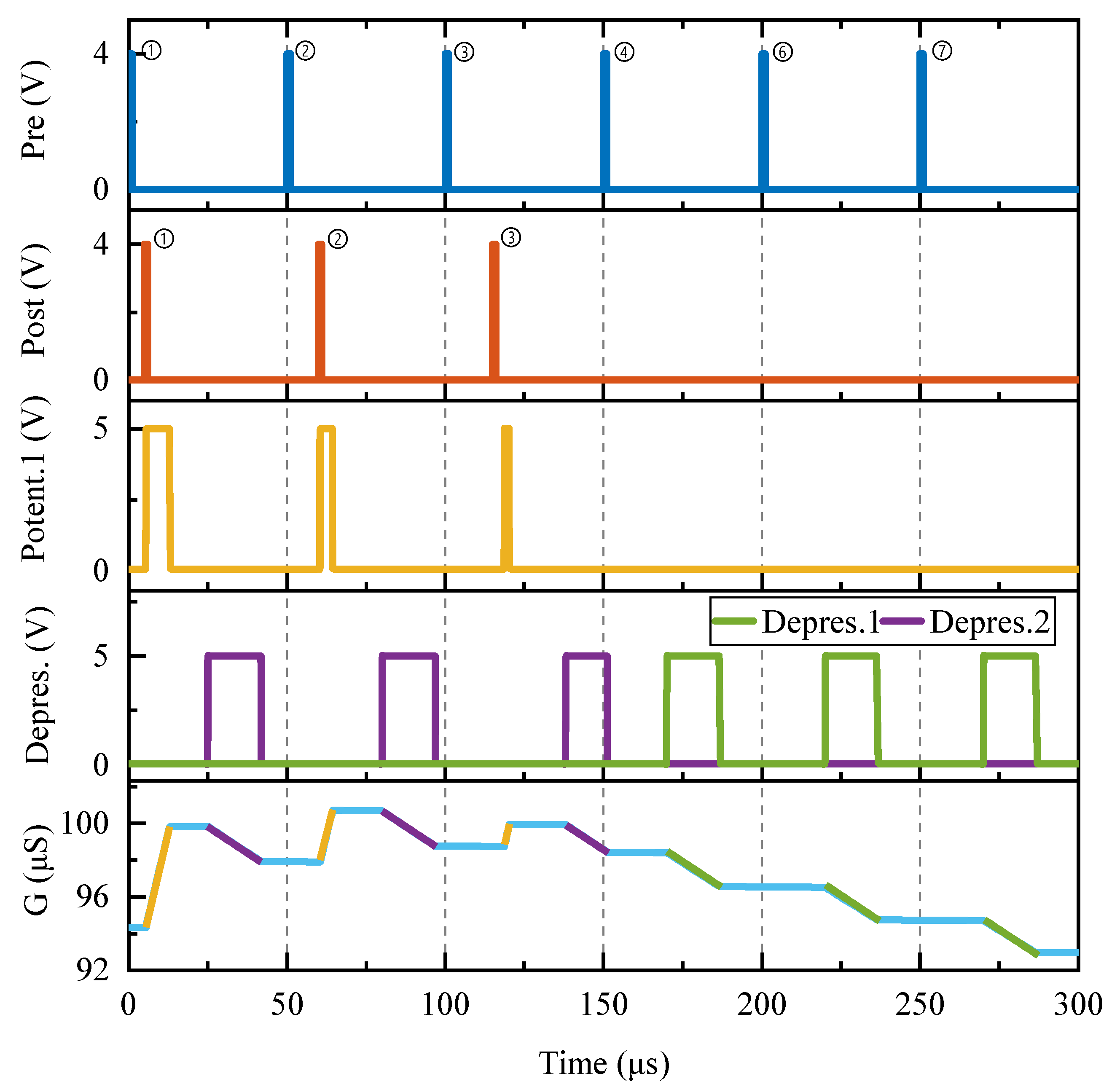
4.2. Applying Continuous Pre- and Postsynaptic Pulses

To further verify the function of the homeostatic inhibitory plasticity rule circuit, pre- and postsynaptic neuronal pulses were continuously applied to the proposed circuit at various time intervals. Figure 13 illustrates the responses of the proposed circuit to continuous pre- and postsynaptic pulses. The time-domain waveforms of Pre, Post, Potentiation1, Depression1, and Depression2, and memristive synaptic conductance are depicted from top to bottom. A Pre is applied every 50 µs, followed by a Post with a 5 µs, 10 µs, and 18 µs delay relative to the Nos. ➀–➂ Pre, respectively.
First, all Posts lag behind Pre by less than 20 µs, causing the enhancement module to output Potentiation1 and the memristive conductance to increase. The longer the Post lags behind the Pre, the narrower the PW of Potentiation1, reducing the rise in memristive conductance relative to its original value (shown in Figure 13 by the yellow line superimposed on the conductance change curve). This conclusion is supported by the ∆t > −20 µs condition depicted in Figure 12b. Second, Nos. ➁–➃ Pre follows behind Nos. ➀–➂ Post by 45 µs, 40 µs, and 32 µs, all of which are greater than 20 µs. As a result, the depression module generates the depression signal Depression2, and the memristive conductance falls, as illustrated by the purple line superimposed on the conductance change curve in Figure 13. It can be concluded that a shorter time PrePost delay results in a smaller reduction in synaptic conductance. Furthermore, the memristive conductance decreases by the same amount after Nos. ➁–➂ Pre because the PWs of the depression signals are the same when the time interval between Pre and Post is greater than or equal to 40 µs. Finally, there is no more Post after Nos. ➃–➆ Pre, which corresponds to a situation where the time interval between Post and Pre is larger than 40 µs; therefore, the memristive conductance will continue to fall by the same amount (as shown by the superimposed green line part on the conductance change curve in Figure 13). In conclusion, the aforementioned time-domain variation properties of the memristive conductance are totally consistent with the homeostatic inhibitory plasticity rule.

4.3. Discussion

In this research, a homeostatic inhibitory plasticity rule circuit with a commercial memristor synapse is demonstrated. The above simulation results also allow us to summarize the following points. First, as shown in Figure 12b, both the learning window and time constant of the proposed circuit are in a microsecond time scale. Thus, the information processing speed of the circuit is approximately one thousand times faster than that of the biological [10], meeting the urgent requirement for neuromorphic hardware with fast computing speed. Second, the Vthr40 us and Vthr20 us control the enable signals of the potentiation and depression modules, as well as the homeostatic learning window. Third, because the maximum pulse width of the potentiation and depression signals determines the maximum change in the memristive conductance, the maximum learning rate for synaptic weight enhancement and depression can be adjusted by modifying the respective values of Vthr and Vthr_Depression. In addition, the model fitting experiment revealed that the homeostatic factor α is determined by the minimum reduction in memristive synaptic conductance. Consequently, changing Vthr_Depression can influence the homeostatic factor α: the bigger the Vthr_Depression, the smaller α, and according to [10,11], the smaller the homeostatic firing rate of the postsynaptic neuron.
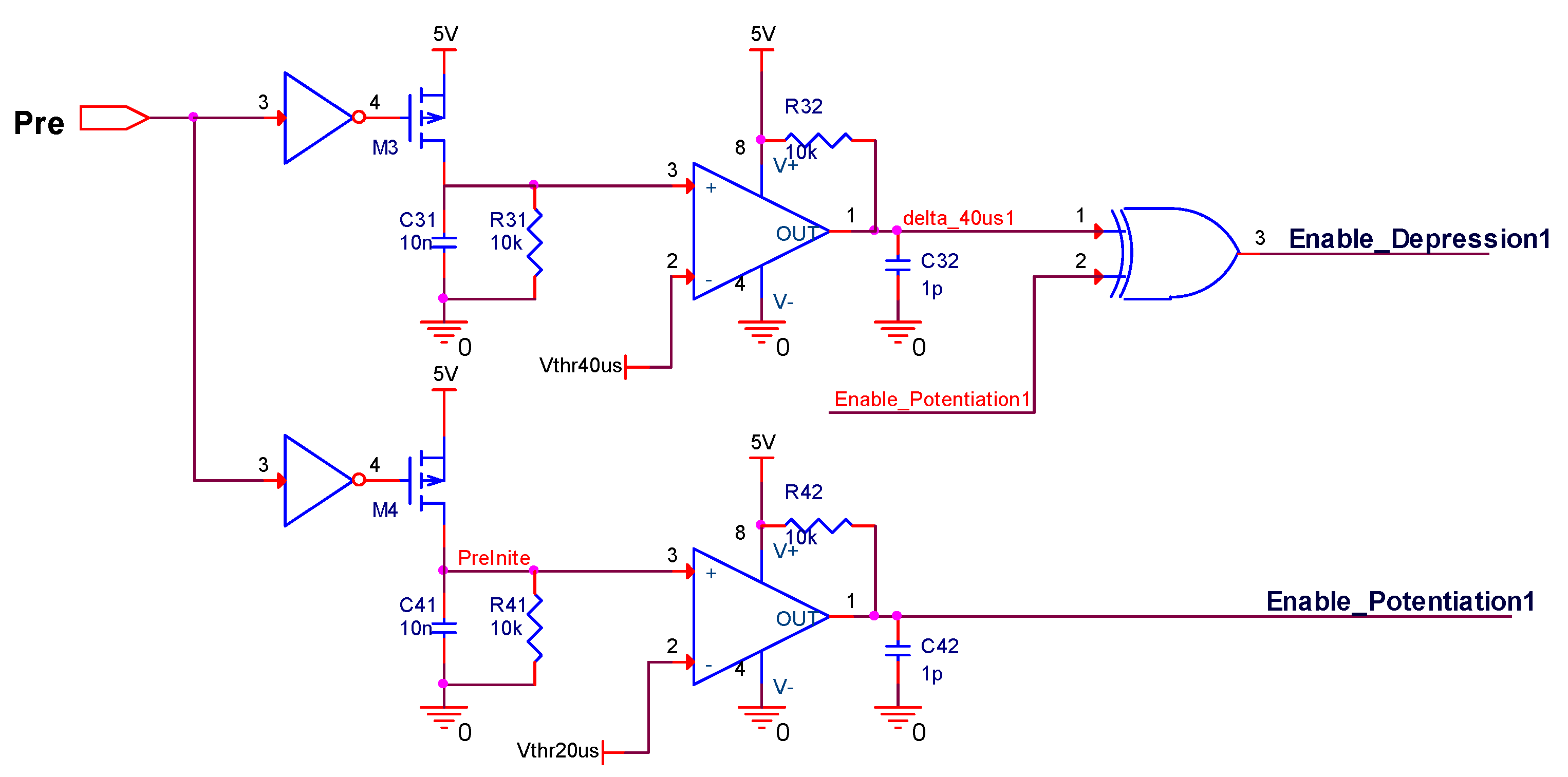
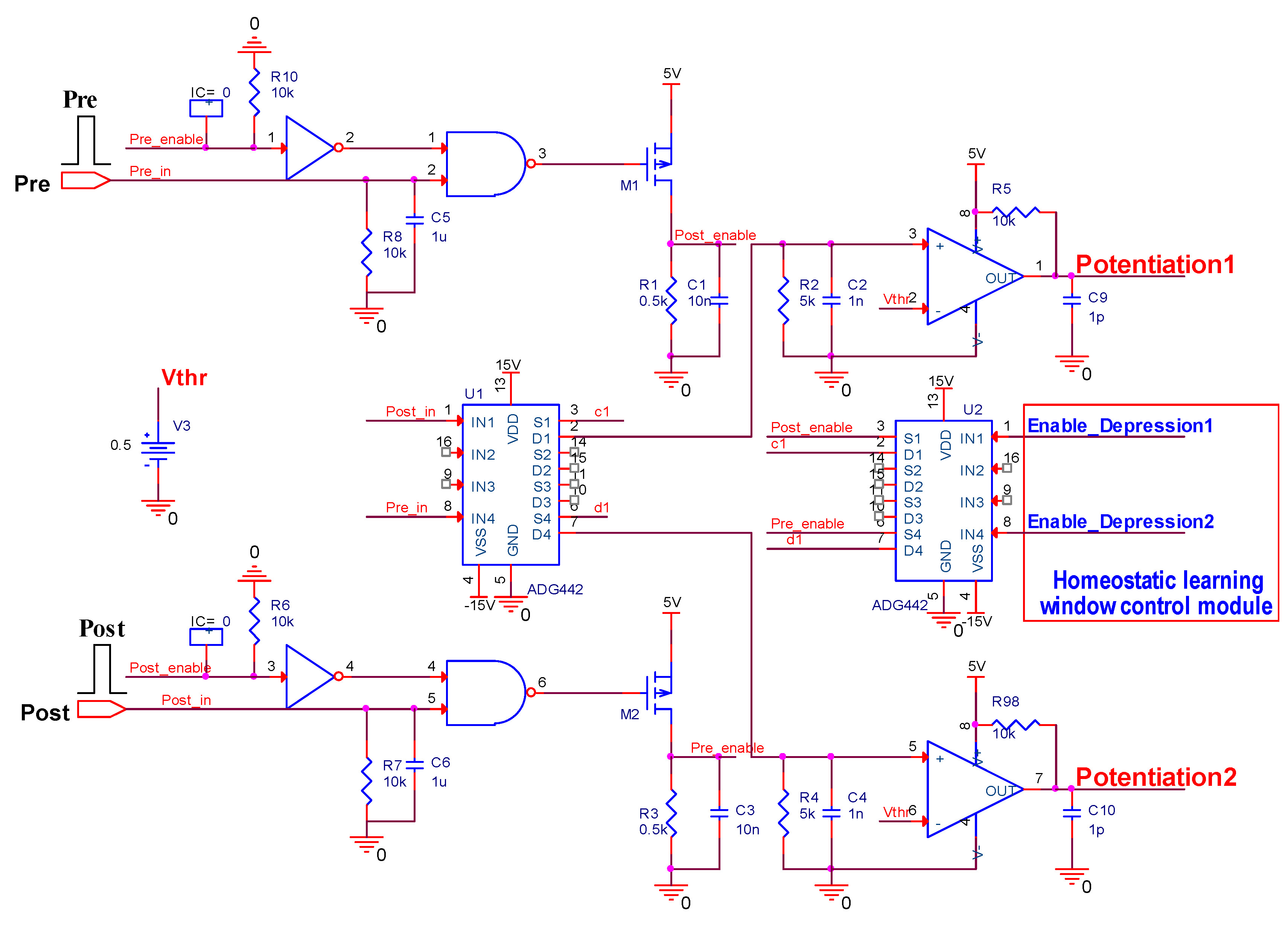
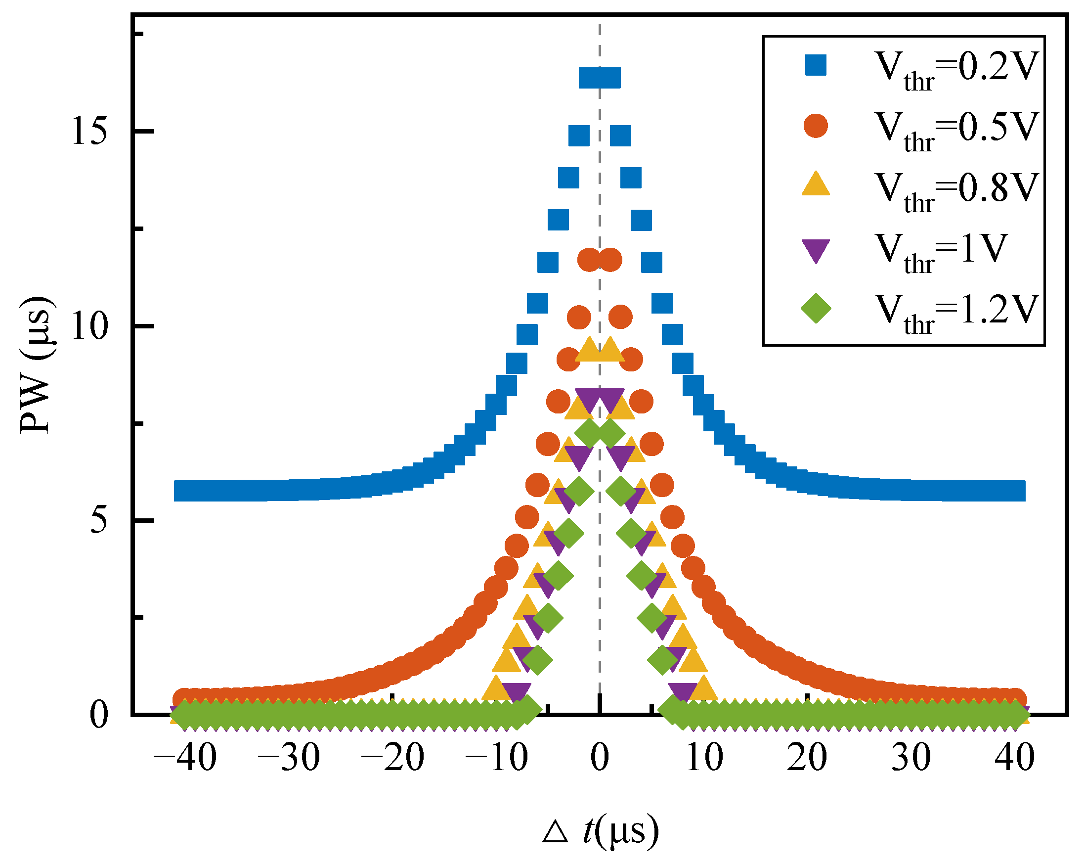
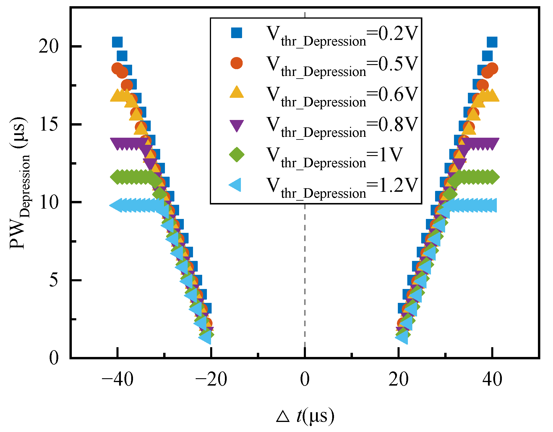
This paper focuses more on the design of a board-level homeostatic inhibitory plasticity rule demonstration circuit. The circuit contains ten MOSFETs, one Knowm memristor, thirty resistors, twenty-eight capacitors, ten inverters, four XOR gates, two AND gates, and ten comparators LM393. Since Pre and Post had high voltages, and comparators, inverters, and gate circuits required high stimulus; together with many large capacitors and resistors, the circuit consumed more power. The total power dissipation of the homeostatic inhibitory plasticity rule circuit estimated using PSpice© was 0.083 W at the displayed power supply. We must admit that this is not a small power dissipation. However, the board-level circuit design in this paper provides an idea for the integrated design of the homeostatic inhibitory plasticity rule circuit. In the nanoscale integrated circuit design field, the input pulse voltage could be appropriately reduced, and the comparator could become smaller and consume less power. Accordingly, the values of the capacitor and resistor used in the design would become smaller, which will be achievable in the near future.
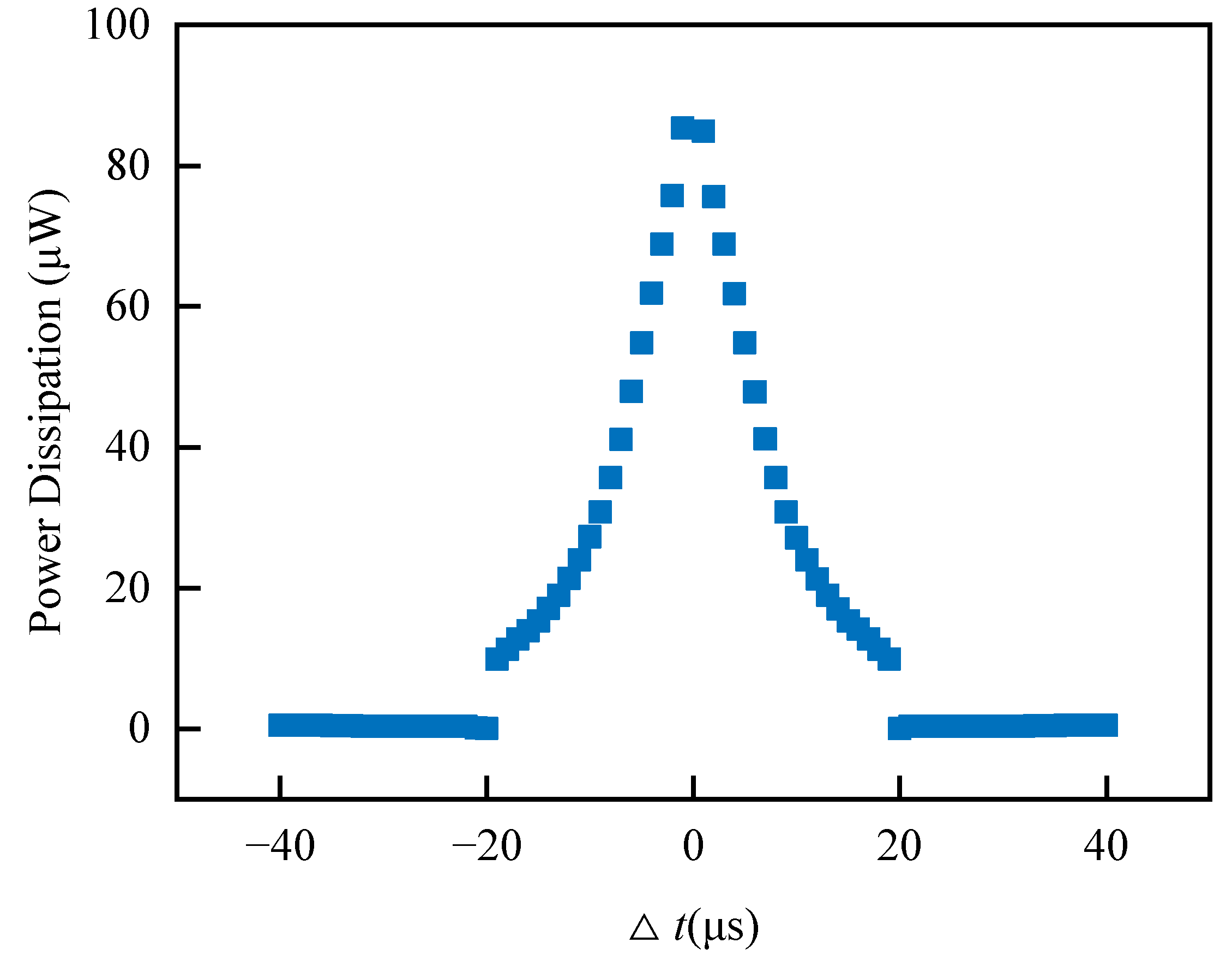
Regardless of the energy consumption of the peripheral control circuit of the memristive synapse, the power consumed by the memristive synapse depends upon the initial state of the memristive conductance, the magnitude of the memristive conductance change, and whether the memristive conductance is increasing or decreasing. Figure 14 depicts the energy consumed by the memristive synapse as a function of the temporal difference between pre- and postsynaptic spikes with the memristive conductance initialized to 94.32 μS. Each point represents the result of a simulation of a single pair of pre- and postsynaptic spikes. The average power consumption for increasing and decreasing synaptic weights is about 35 μW and 0.34 μW, respectively. The Knowm memristive synapse consumes an average of 17.2 μW of power and 0.86 μJ of energy per spike for a spike rate of 20 MHz. Although the energy consumption of this synapse is greater than that of synapses in [20,25], achieving the homeostatic inhibitory plasticity rule for the first time is very meaningful based on a commercial memristor. It also suggests that reducing its power consumption will be one of the following tasks we will implement.

5. Conclusions

In this study, a fast homeostatic inhibitory plasticity rule circuit with a commercial memristor synapse is proposed and verified in PSpice© for the first time. The simulation results indicate that the circuit successfully implements the homeostatic inhibitory plasticity rule, and its time scale is one thousand times quicker than biology. This meets the requirements of neuromorphic hardware for fast computing speed. Moreover, the proposed circuit is promising for a wide range of applications with an adjustable steady-state learning window, learning rate, and steady-state factor. This research offers the groundwork for developing neuromorphic technology with homeostatic firing rates, similar to those of the biological nervous system. In addition, we believe that implementing the homeostatic inhibitory plasticity rule in the design of neuromorphic hardware can improve its reliability. This hypothesis will be verified in our upcoming study.

Author Contributions

Conceptualization, G.M. and S.L.; data curation, Y.Z.; formal analysis, G.M.; funding acquisition, M.M.; investigation, G.M. and Y.Z.; methodology, G.M.; project administration, M.M. and S.L.; resources, G.M.; software, G.M. and M.M.; validation, G.M. and Y.Z.; writing—original draft, G.M.; writing—review and editing, G.M. and S.L. All authors have read and agreed to the published version of the manuscript.

Funding

This research was funded by the National Defense Basic Scientific Research Plan of China(Grant number: JCKY2020DC202) and the National Natural Science Foundation of China, (Grant number: 51407194).

Data Availability Statement

Not applicable.

Conflicts of Interest

The authors declare no conflict of interest.

Appendix A

.SUBCKT MEM_KNOWM TE BE XSV PARAMS:
+Ron = 5880 Roff = 44020 Voff = 0.17 Von = 0.37 TAU = 0.0001 VT = 26m x0 = 0.5
Cx XSV 0 {1}
.ic V(XSV) = {x0}
Gx 0 XSV value = {F(V(TE,BE),V(XSV,0))}
Gm TE BE value = {IVRel(V(TE,BE),V(XSV,0))}
Raux XSV 0 1T
* Memristor I–V Relationship
.func IVRel(V1,V2) = {V1*G(V2)}
* Circuit to determine state variable
* Function G(V(t))
.func G(V) = {V/Ron + (1−V)/Roff}
.func F(V1,V2) = {(1/TAU)*((1/(1 + exp(−1/(VT)*(V1−Von))))
+ *(1−V2) − (1− (1/(1 + exp(−1/(VT)*(V1 + Voff)))))*V2)}
.ENDS

References

  1. Mead, C. Neuromorphic electronic systems. Proc. IEEE 1990, 78, 1629–1636. [Google Scholar] [CrossRef] [Green Version]
  2. Young, A.R.; Dean, M.E.; Plank, J.S.; Rose, G.S. A review of spiking neuromorphic hardware communication systems. IEEE Access 2019, 7, 135606–135620. [Google Scholar] [CrossRef]
  3. Boybat, I.; Le Gallo, M.; Nandakumar, S.R.; Moraitis, T.; Parnell, T.; Tuma, T.; Rajendran, B.; Leblebici, Y.; Sebastian, A.; Eleftheriou, E. Neuromorphic computing with multi-memristive synapses. Nat. Commun. 2018, 9, 2514. [Google Scholar] [CrossRef] [Green Version]
  4. Schuman, C.D.; Potok, T.E.; Patton, R.M.; Birdwell, J.D.; Dean, M.E.; Rose, G.S.; Plank, J.S. A Survey of Neuromorphic Computing and Neural Networks in Hardware. arXiv 2017, arXiv:1705.06963. [Google Scholar]
  5. Gaol, D.; Zhang, G.L.; Yin, X.; Li, B.; Schlichtmann, U.; Zhuo, C. Reliable Memristor-based Neuromorphic Design Using Variation- and Defect-Aware Training. In Proceedings of the 2021 IEEE/ACM International Conference On Computer Aided Design, Munich, Germany, 1–4 November 2021. [Google Scholar]
  6. Zhao, M.; Gao, B.; Tang, J.; Qian, H.; Wu, H. Reliability of analog resistive switching memory for neuromorphic computing. Appl. Phys. Rev. 2020, 7, 11301. [Google Scholar] [CrossRef]
  7. Davis, G.W. Homeostatic control of neural activity: From Phenomenology to Molecular Design. Annu. Rev. Neurosci. 2006, 29, 307–323. [Google Scholar] [CrossRef] [Green Version]
  8. Voicu, H.; Mauk, M.D. No neuron is an island: Homeostatic plasticity and over-constraint in a neural circuit. Neurobiol. Learn. Mem. 2019, 170, 106982. [Google Scholar] [CrossRef] [PubMed]
  9. Turrigiano, G.G.; Nelson, S.B. Homeostatic plasticity in the developing nervous system. Nat. Rev. Neurosci. 2004, 5, 97–107. [Google Scholar] [CrossRef]
  10. Vogels, T.P.; Sprekeler, H.; Zenke, F.; Clopath, C.; Gerstner, W. Inhibitory plasticity balances excitation and inhibition in sensory pathways and memory networks. Science 2011, 334, 1569–1573. [Google Scholar] [CrossRef] [Green Version]
  11. Vogels, T.P.; Froemke, R.C.; Doyon, N.; Gilson, M.; Haas, J.S.; Liu, R.; Maffei, A.; Miller, P.; Wierenga, C.; Woodin, M.; et al. Inhibitory synaptic plasticity: Spike timing-dependence and putative network function. Front. Neural Circuit 2013, 7, 119. [Google Scholar] [CrossRef] [Green Version]
  12. Turrigiano, G. Homeostatic synaptic plasticity: Local and global mechanisms for stabilizing neuronal function. Cold Spring Harb. Perspect. Biol. 2012, 4, a005736. [Google Scholar] [CrossRef] [PubMed]
  13. Desai, N.S. Homeostatic plasticity in the CNS: Synaptic and intrinsic forms. J. Physiol. Paris 2003, 97, 391–402. [Google Scholar] [CrossRef] [PubMed]
  14. Hengen, K.B.; Lambo, M.E.; Van Hooser, S.D.; Katz, D.B.; Turrigiano, G.G. Firing Rate Homeostasis in Visual Cortex of Freely Behaving Rodents. Neuron 2013, 80, 335–342. [Google Scholar] [CrossRef] [PubMed] [Green Version]
  15. Li, Y.; Zhong, Y.; Xu, L.; Zhang, J.; Xu, X.; Sun, H.; Miao, X. Ultrafast synaptic events in a chalcogenide memristor. Sci. Rep. 2013, 3, 1619. [Google Scholar] [CrossRef] [PubMed] [Green Version]
  16. Yang, R.; Huang, H.M.; Guo, X. Memristive synapses and neurons for bioinspired computing. Adv. Electron. Mater. 2019, 5, 1900287. [Google Scholar] [CrossRef]
  17. Choi, S.; Yang, J.; Wang, G. Emerging Memristive Artificial Synapses and Neurons for Energy-Efficient Neuromorphic Computing. Adv. Mater. 2020, 32, 2004659. [Google Scholar] [CrossRef]
  18. Cruz-Albrecht, J.M.; Yung, M.W.; Srinivasa, N. Energy-efficient neuron, synapse and STDP integrated circuits. IEEE Trans. Biomed. Circuits Syst. 2012, 6, 246–256. [Google Scholar] [CrossRef]
  19. Zhang, X.; Xia, T.; Ye, C.; Liu, Y.X.; Liu, L.; Shen, L.P. Realizing diverse STDP learning rules in synaptic circuit based on memristor. Sci. Sin. Technol. 2021, 51, 89–98. [Google Scholar] [CrossRef]
  20. Zhou, W.; Wen, S.; Liu, Y.; Liu, L.; Liu, X.; Chen, L. Forgetting memristor based STDP learning circuit for neural networks. Neural Netw. 2022, 158, 293–304. [Google Scholar] [CrossRef]
  21. Campbell, K.A. Self-directed channel memristor for high temperature operation. Microelectron. J. 2017, 59, 10–14. [Google Scholar] [CrossRef]
  22. Self Directed Channel Memristors. Available online: https://Knowm.org/downloads/Knowm_Memristors.pdf (accessed on 20 December 2022).
  23. Zhu, L.; Wang, F. Design and analysis of new meminductor model based on KNOWM memristor. Acta Phys. Sin. 2019, 68, 275–281. [Google Scholar] [CrossRef]
  24. Ma, G.; Man, M.; Zhang, Y.; Liu, S. Electromagnetic Interference Effects of Continuous Waves on Memristors: A Simulation Study. Sensors 2022, 22, 5785. [Google Scholar] [CrossRef] [PubMed]
  25. Ivans, R.C.; Cantley, K.D.; Shumaker, J.L. A CMOS synapse design implementing tunable asymmetric spike timing-dependent plasticity. In Proceedings of the 2017 IEEE 60th International Midwest Symposium on Circuits and Systems (MWSCAS), Boston, MA, USA, 6–9 August 2017. [Google Scholar]
Figure 1. Schematic diagram of the homeostatic inhibitory plasticity rule curve.
Electronics 12 00490 g001
Figure 2. The Knowm memristor PSpice© model: (a) model symbol; (b) model structure.
Electronics 12 00490 g002
Figure 3. Block diagram of the homeostatic inhibition plasticity rule circuit.
Electronics 12 00490 g003
Figure 4. Circuit schematic of the homeostatic learning window control module.
Electronics 12 00490 g004
Figure 5. The enable signals output by the homeostatic learning window control module circuit.
Electronics 12 00490 g005
Figure 6. Circuit schematic of the potentiation module.
Electronics 12 00490 g006
Figure 7. PW of potentiation signals changing with ∆t at different Vthr.
Electronics 12 00490 g007
Figure 8. Circuit schematic of the depression module.
Electronics 12 00490 g008
Figure 9. The time-domain waveforms of several significant node voltages inside the Depression2 generating circuit.
Electronics 12 00490 g009
Figure 10. PW of depression signals changing with ∆t at different Vthr_Depression.
Electronics 12 00490 g010
Figure 11. Circuit schematic of the weight update module.
Electronics 12 00490 g011
Figure 12. PSpice© simulation results after traversing Δt. (a) Memristor’s state variable x; (b) the change in memristive synaptic conductance with ∆t.
Electronics 12 00490 g012
Figure 13. Responses of the proposed circuit to continuous pre- and postsynaptic pulses. The time-domain waveforms of Pre, Post, Potentiation1, Depression1 and Depression2, and memristive synaptic conductance are depicted from top to bottom.
Electronics 12 00490 g013
Figure 14. Power consumption by the synapse as a function of the temporal difference between pre- and postsynaptic spikes.
Electronics 12 00490 g014
Disclaimer/Publisher’s Note: The statements, opinions and data contained in all publications are solely those of the individual author(s) and contributor(s) and not of MDPI and/or the editor(s). MDPI and/or the editor(s) disclaim responsibility for any injury to people or property resulting from any ideas, methods, instructions or products referred to in the content.

