Communication

Ti/HfO2-Based RRAM with Superior Thermal Stability Based on Self-Limited TiOx

1
China Nanhu Academy of Electronics and Information Technology, Jiaxing 314001, China
2
Institute of Advanced Technology, University of Science and Technology of China, Hefei 230026, China
3
College of Information Science and Electronic Engineering, Zhejiang University, Hangzhou 310058, China
4
School of Integrated Circuits, East China Normal University, Shanghai 200241, China
*
Author to whom correspondence should be addressed.
Electronics 2023, 12(11), 2426; https://doi.org/10.3390/electronics12112426
Submission received: 18 April 2023 / Revised: 23 May 2023 / Accepted: 23 May 2023 / Published: 26 May 2023
(This article belongs to the Special Issue Advanced CMOS Devices and Applications)

Abstract

:
HfO2-based resistive random-access memory (RRAM) with a Ti buffer layer has been extensively studied as an emerging nonvolatile memory (eNVM) candidate because of its excellent resistive switching (RS) properties and CMOS process compatibility. However, a detailed understanding of the nature of Ti thickness-dependent RS and systematic thermal degradation research about the effect of post-metallization annealing (PMA) time on oxygen vacancy distribution and RS performance still needs to be included. Herein, the impact of Ti buffer layer thickness on the RS performance of the Al/Ti/HfO2/TiN devices is first addressed. Consequently, we have proposed a simple strategy to regulate the leakage current, forming voltage, memory window, and uniformity by varying the thickness of the Ti layer. Moreover, it is found that the device with 15 nm Ti shows the minimum cycle-to-cycle variability (CCV) and device-to-device variability (DDV), good retention (105 s at 85 °C), and superior endurance (104). In addition, thermal degradation of the Al/Ti(15 nm)/HfO2/TiN devices under different PMA times at 400 °C is carried out. It is found that the leakage current increases and the forming voltage and memory window decrease with the increase in PMA time due to the thermally activated oxidation of the Ti. However, when the PMA time increases to 30 min, the Ti can no longer capture oxygen from HfO2 due to the formation of self-limited TiOx. Therefore, the device shows superior thermal stability with a PMA time of 90 min at 400 °C and no degradation of the memory window, uniformity, endurance, or retention. This work demonstrates that the Ti/HfO2-based RRAM shows superior back-end-of-line compatibility with high thermal stability up to 400 °C for over an hour.

1. Introduction

Recently, RRAM based on transition metal oxides (TMOs) has attracted increasing attention as one of the most promising candidates for the next generation of eNVM because of its prominent advantages, including its low cost, high integration density, fast switching speed, high endurance, and good CMOS process compatibility [1,2,3,4,5,6,7,8,9]. In recent decades, RS characteristics have been observed and extensively investigated in various TMOs such as HfO2, TaOx, TiO2, AlOx, NiOx, and ZrOx [10,11,12,13,14,15]. Among these TMOs, HfO2 is one of the most representative candidates owing to its high endurance, fast switching speed, and excellent thermal stability [10,16,17].
However, HfO2 deposited by atomic layer deposition (ALD) tends to be a stoichiometric film with few defects or vacancies, resulting in high forming voltage and hard breakdown during the forming operation [10]. This forming process, which involves the application of a voltage typically higher than the operation voltage, induces worse RS performance, larger power consumption, and an additional burden on circuit design. Therefore, to increase the initial oxygen vacancy concentration in the HfO2 to reduce the forming voltage and improve the RS performance, reactive metals such as Ta, Ti, and Hf are generally introduced on the top of the HfO2 layer as oxygen-scavenging metals [18]. Up to now, excellent RS properties, including superior endurance (1010), good retention characteristics (10 years at room temperature), and low switching energy (0.1 pJ per bit operation), have been demonstrated in Ti/HfO2-based RRAM [19,20]. Although the importance of the Ti buffer layer is well understood, the detailed interpretation of Ti thickness-dependent RS has not been fully understood, which significantly limits its applications. Recently, other researchers have found that the leakage current increases and the forming voltage decreases as the Ti thickness increases, and the RS properties can be regulated by changing the Ti thickness [21,22,23]. However, due to the insufficient thickness of the Ti layer, the saturation of the leakage current and the forming voltage with increasing Ti thickness was not observed, resulting in some interesting phenomena being missed. In addition, the effect of the Ti thickness on the RS uniformity has yet to be investigated. Therefore, it is urgent to comprehensively reveal the relationship between Ti thickness and oxygen vacancy concentration in the HfO2 layer and regulate the RS behavior by changing Ti thickness.
Notably, both the fabrication process of the RRAM device and the post-RRAM process need to be carried out at 400 °C. Furthermore, since HfO2-based devices operate based on the formation/fracture of conductive filaments originating from the migration of oxygen vacancies, they are vulnerable to structural defects caused by the heat applied during the annealing process. Therefore, to enable the mass production of RRAM, it is critical to meet the thermal budget requirements of the CMOS process. However, most research on HfO2-based RRAM has focused on improving the RS characteristics of the device. In contrast, there are few reports on the impact of the PMA process on RS performance [24]. Additionally, the cumulative duration of the post-RRAM thermal process, including chemical vapor deposition, rapid thermal annealing, ALD, furnace annealing, and UV curing, usually exceeds one hour. However, up to now, most of the reported thermal stability tests have lasted less than or equal to one hour [25,26,27,28,29]. More importantly, there is no systematic research about the effect of PMA time on oxygen vacancy distribution and RS properties.
In this work, the HfO2-based RRAM devices with different thicknesses of Ti buffer layer are fabricated. It is found that the leakage current, forming voltage, memory window, and uniformity can be regulated by varying the thickness of the Ti buffer layer. Owing to the low forming voltage, the device with 15 nm Ti presents superior uniformity, good retention, and excellent endurance. In addition, the Al/Ti(15 nm)/HfO2/TiN devices with different PMA times at 400 °C are compared and analyzed. It is found that the leakage current (the forming voltage and ON/OFF ratio) increases (decrease) with the increase of the PMA time and remains unchanged when the PMA time increases to 30 min due to the formation of self-limited TiOx. More importantly, the memory window, uniformity, endurance, and retention show no obvious degradation with a PMA time of 90 min at 400 °C, indicating superior thermal stability of the present devices.

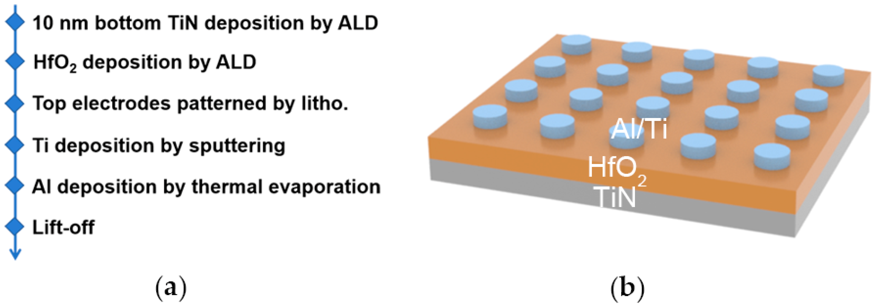
2. Materials and Methods

The fabrication process of the Al/Ti/HfO2/TiN devices is described in Figure 1a. To fabricate the Al/Ti/HfO2/TiN devices, 15 nm TiN was first deposited on the heavily doped Si as the bottom electrode by ALD. The precursors used for TiN deposition are ammonia and titanium tetrachloride. Subsequently, pure HfO2 with a thickness of 8 nm was deposited by ALD using tetrakis(dimethylamino)hafnium (TDMAHf) and H2O as precursors. The chamber temperature was set at 250 °C. After the HfO2 deposition, five different thicknesses of the Ti buffer layer (0, 5, 10, 15, and 20 nm) on top of the HfO2 layer were deposited by the sputtering system. Al capping layer with a thickness of 80 nm to protect Ti from oxidation was then deposited by thermal evaporation using the same sputtering system without breaking the vacuum. The TE layer (Al/Ti) was patterned via the lift-off process. Finally, PMA was performed for 0, 10, 15, 30, 60, and 90 min at 400 °C in the N2 atmosphere. The schematic of the prepared Al/Ti/HfO2/TiN devices is shown in Figure 1b.
X-ray photoelectron spectroscopy (XPS) characterizations were performed using a Kratos Axis Ultra system to analyze the chemical states of the samples with a monochromated Al anode. The source operated at a voltage of 14 kV and an emission of 8 mA. The vacuum of the analysis chamber was higher than 5 × 10⁻⁹ Torr before measurements. The binding energies were calibrated for the sample charging effect by referencing the C 1s peak at 284.8 eV. Before XPS characterization, the TiOx on the surface was first removed by Ar sputtering in the load lock chamber. To ensure consistency between different samples, special attention needs to be paid to keeping the etching time constant (5 s). The etching rate was roughly 0.7 nm/s.
An Agilent B1500A semiconductor parameter analyzer conducted electrical measurements in the atmospheric ambient. The voltage bias was applied to the top electrode while the bottom electrode was grounded.

3. Results

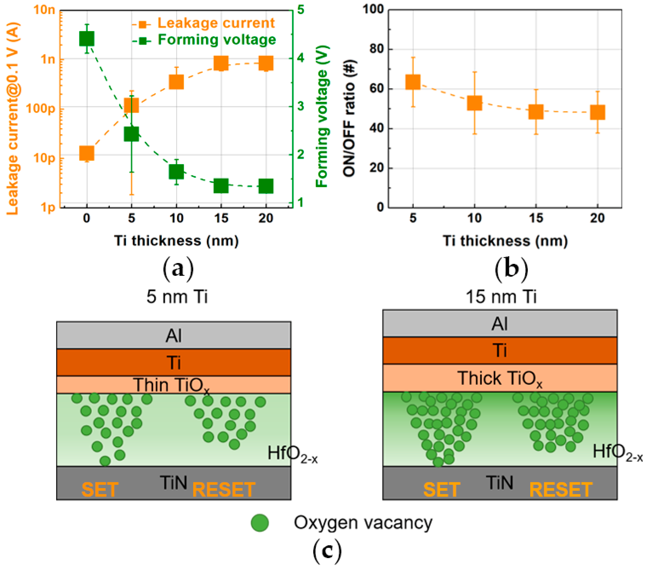
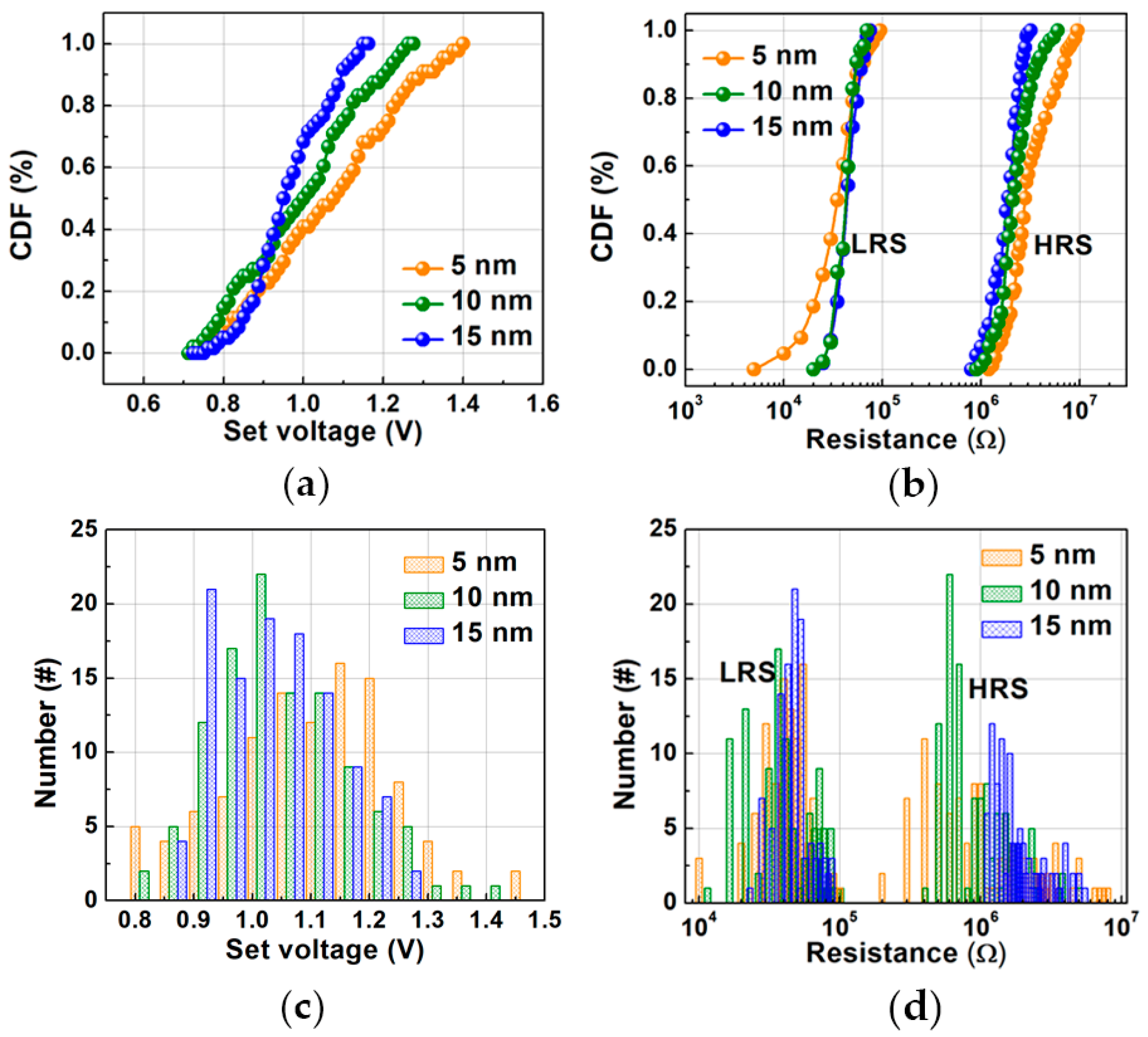
3.1. Ti Thickness-Dependent RS

In order to reveal the effect of Ti buffer layer thickness on the RS performance, electrical properties, including leakage current (Jg), forming voltage (Vf), and ON/OFF ratio of the Al/Ti/HfO2/TiN devices with different Ti thicknesses, are displayed in Figure 2. The Jg represents the current measured at the initial resistance with a read voltage of 0.1 V. Notably, over 20 devices were tested for each structure to compare. As shown in Figure 2a, the mean values of Jg of the Al/Ti/HfO2/TiN devices with five different Ti thicknesses (0, 5, 10, 15, and 20 nm) are 1.27 × 10⁻¹¹, 1.18 × 10⁻¹⁰, 3.52 × 10⁻¹⁰, 8.48 ×10⁻¹⁰, and 8.45 ×10⁻¹⁰ A, respectively. Correspondingly, the Vf values are 4.4, 2.4, 1.6, 1.35, and 1.35 V, respectively. It is found that Jg increases and Vf decreases as the Ti thickness increases due to the high oxygen-gettering ability of the Ti. When the Ti thickness increases from 0 to 15 nm, more oxygen vacancies in the HfO2 are introduced, resulting in a higher Jg and a lower Vf. However, Jg and Vf remain almost unchanged when the Ti thickness increases from 15 to 20 nm. It can probably be explained that the oxidation of Ti is self-limiting and that the oxygen vacancy concentration in HfO2 reaches a constant value. Yang et al. demonstrated that self-limiting oxidation comes from the residual compressive stress in TiO2 [30]. When the potential barrier resulting from compressive deformation is higher than the activation energy of oxygen diffusion and reaction, self-limiting oxidation occurs.
After the forming process, bipolar RS behaviors were obtained, where the device could be SET (the switching from high resistance state (HRS) to low resistance state (LRS)) after the positive voltage sweeping and RESET (the switching from LRS to HRS) after the negative voltage sweeping. Figure 2b shows the ON/OFF ratio distribution of the Al/Ti/HfO2/TiN devices with different Ti thicknesses. Notably, the ON/OFF ratio cannot be obtained in the device without the Ti buffer layer, since no RS was observed after the forming process. It is found that the ON/OFF ratio shows a slight decrease when the Ti thickness increases from 5 to 15 nm, which suggests that the initially created oxygen vacancies also play a vital role in switching cycles. Moreover, the ON/OFF ratio remains almost unchanged when the Ti thickness exceeds 15 nm due to the formation of self-limited TiOx.
Based on the above experimental results, schematic diagrams of the generalized model to understand the role of Ti thickness in the RS performance of the present devices are shown in Figure 2c. When a thin Ti layer is inserted on top of the HfO2, the RS behavior is generally unstable due to the higher Vf originating from pre-existing oxygen vacancies. Note that more oxygen vacancies are introduced in the HfO2 layer, and a lower Vf can be obtained by selecting a thick Ti layer (15 nm). However, the ON/OFF ratio decreases (see Figure 2b), which may result from the shorter oxygen vacancy gap region during switching cycles compared to the sample with a thin Ti layer.
Additionally, to further investigate the effect of Ti buffer layer thickness on the RS uniformity, the CCV and DDV of the Al/Ti/HfO2/TiN devices with different thicknesses of the Ti buffer layer (5, 10, and 15 nm) are displayed in Figure 3. It is worth noting that the data for the devices with 20 nm Ti is not displayed in Figure 3, since the devices with 20 nm Ti exhibited a similar RS behavior to those with 15 nm Ti. Regarding the extraction of SET voltage (VSET), we employ a numerical technique that identifies the voltage at which a sudden change occurs in the current. This abrupt transition signifies the initiation of the SET process. In contrast, the LRS and HRS are determined by measuring the resistance values at 0.1 V after the completion of the SET and RESET processes, respectively. Figure 3a,b present the statistical distribution of VSET, LRS, and HRS obtained by 100 dc sweep cycles. It can be clearly observed that the sample with a thicker Ti buffer layer shows improved control of tail bits in the distribution of VSET, HRS, and LRS, indicating that the device with a 15 nm Ti buffer layer exhibits a minimum CCV. In addition, we statistically analyze 200 I-V curves collected in 10 devices for each device with different Ti thicknesses (5, 10, and 15 nm) and quantify the DDV of the VSET, HRS, and LRS by calculating the coefficient of variation (CV) as the standard deviation (σ) divided by the mean value (μ). As displayed in Figure 3c,d, both VSET, HRS, and LRS follow a Gaussian distribution:
y = y 0 + A × e x p ( x μ 2 2 σ 2 ) ,
where y0 and A are constants, μ is the expectation, representing the mean value of the voltage, and σ is the standard deviation, representing the concentration of the voltage distribution. CV is the ratio of σ and μ, reflecting the concentration of the distribution. Furthermore, the VSET, HRS, and LRS of the device with 15 nm Ti show the narrowest distribution, and the DDV of the VSET, HRS, and LRS is 12.85%, 17.07%, and 17.16%, respectively. The above results demonstrate that the device with a 15 nm Ti shows the best RS uniformity, which may originate from the initial high oxygen vacancy concentration, reduced forming voltage, and TiOx formation [26,31].
Since the HfO2-based RRAM device with a 15 nm Ti buffer layer shows the best uniformity, the RS behaviors of the present devices are systematically investigated, as displayed in Figure 4. After the application of a forming voltage (~1.3 V), the present device exhibited stable bipolar RS behavior when the voltage was swept between −1.5 V and 1.5 V, as displayed in Figure 4a. While a continuous voltage swept from 0 V to 1.5 V→−1.5 V→0 V, an obvious hysteresis loop was obtained, where SET occurred at about 1 V and RESET happened at about −1 V. It is worth noting that a compliance current of 50 μA was applied during the forming and SET processes to prevent irreversible breakdown, while no compliance current was applied during the RESET process. This hysteresis behavior is reproducible in the consecutive 100 voltage sweeps, demonstrating stable RS characteristics in the Al/Ti/HfO2/TiN devices. The retention characteristics were measured at 85 °C, as shown in Figure 4b. The ON/OFF ratio is larger than 50, and the current values of the HRS and LRS show no degradation within 105 s, indicating superior retention characteristics.
In addition to stable bipolar RS behavior and good retention characteristics, the present device exhibits superior endurance. When one sequence of SET (1.2 V, 1 μs), read (0.1 V, 30 ms), RESET (−1.5 V, 10 μs), and read (0.1 V, 50 ms) pulses was applied, it was observed that the current value after the SET pulse is several tens of times that of the current value after the RESET pulse (see Figure 4c), demonstrating the presence of the RS behavior. To obtain the endurance for one cycle, one can record one current data point in each read pulse. By repeatedly applying the above pulse sequence, an endurance plot showcasing the current levels of HRS and LRS for 104 cycles was achieved (see Figure 4d), indicating the superior endurance of the present device.

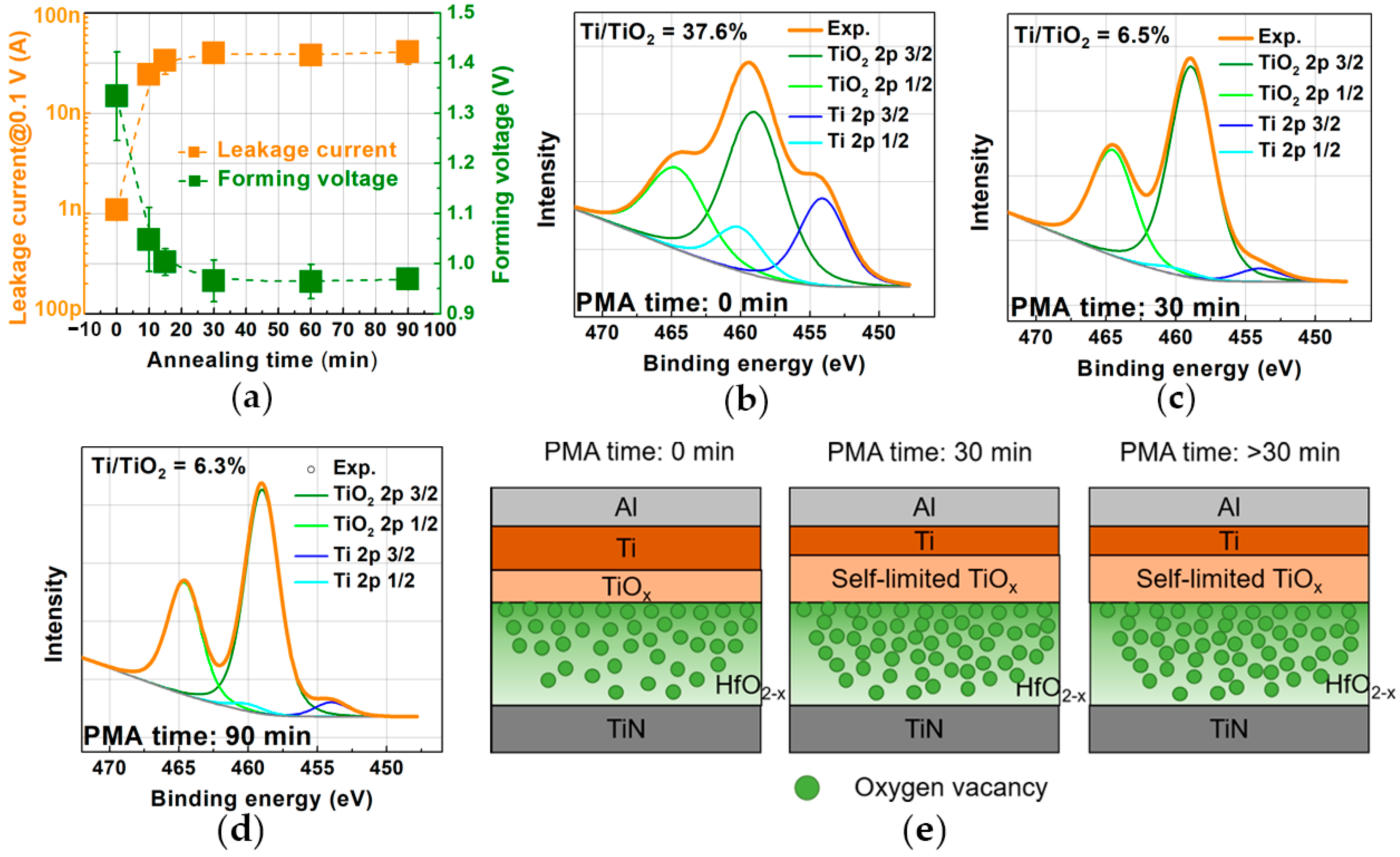
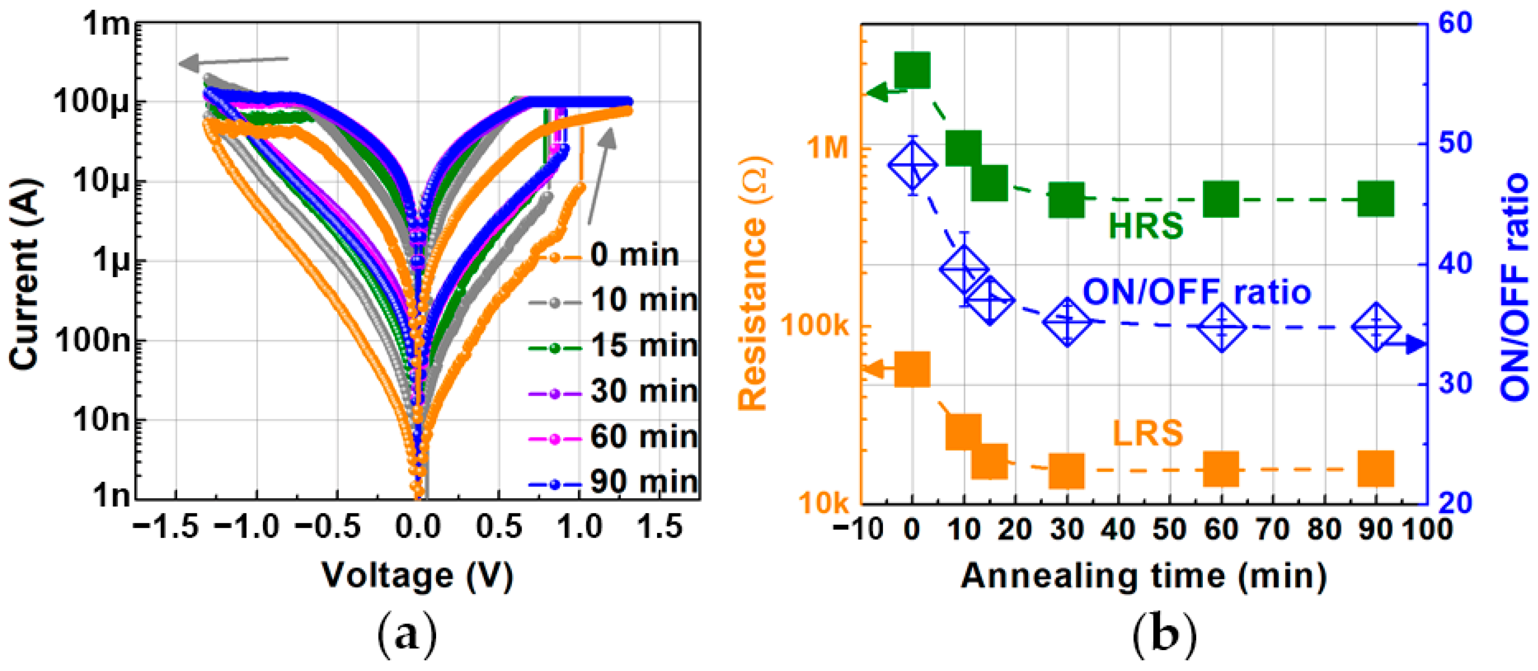
3.2. Systematic Thermal Degradation Research about the Effect of PMA Time on Oxygen Vacancy Distribution and RS Performance

The electrical properties of the Al/Ti(15 nm)/HfO2 /TiN devices with different PMA times were compared and analyzed to investigate the thermal budget effects on the RS characteristics. Figure 5a presents the distribution of Jg and Vf of the Al/Ti(15 nm)/HfO2 /TiN devices with increasing PMA time from 0 to 90 min. The mean values of Vf in the present devices with increasing PMA times (0, 10, 15, 30, 60, and 90 min) are 1.35, 1.05, 1.00, 0.96, 0.96, and 0.96 V, respectively. Correspondingly, the Jg values are 1.1 × 10⁻⁹, 2.44 × 10⁻⁸, 3.36 × 10⁻⁸, 4.00 ×10⁻⁸, 3.77 ×10⁻⁸, and 4.09 ×10⁻⁸ A, respectively. Notably, for the devices with PMA for over 30 min, the Vf (0.96 V) is close to the VSET (0.9–1.0 V), indicating that the devices show forming-free characteristics. It is obvious that Jg increases and Vf decreases with the increase of the PMA time from 0 to 30 min due to thermally activated oxidation of the Ti buffer layer. However, Jg and Vf remain almost unchanged when the PMA time is over 30 min, which indicates that self-limiting oxidation has occurred.
Furthermore, to demonstrate the occurrence of self-limiting oxidation, XPS characterizations were employed to reveal the atomic composition changes of Ti on the surface of three samples with the structure of Ti/HfO2/TiN using PMA times of 0, 30, and 90 min. Notably, the TiOx on the surface is first removed by Ar sputtering in the load lock chamber of the XPS system. Figure 5b–d show the normalized Ti 2p core-level spectra of three samples with increased PMA time. Quantitative peak analysis was performed by fitting spin-orbit splitting components with Doniach Sunjic (Ti) and Gaussian-Lorentzian (TiO2) line shapes to the spectrum. Each Ti 2p orbital doublet peak was fitted with an area ratio of 1:2, and the spin orbit splitting of Ti and TiO2 was 6.1 eV and 5.60 eV, respectively, consistent with the values in the literature [32]. To highlight the changes in the Ti oxidation among these three samples, the ratio between the Ti and the TiO2 intensity was calculated and further expressed as Ti/TiO2. When the PMA time increases from 0 to 30 min, the Ti/TiO2 ratio decreases from 37.6% to 6.5%, demonstrating enhanced Ti oxidation at the Ti/HfO2 interface because of the thermally activated oxidation of the Ti. More importantly, the Ti/TiO2 ratio is nearly unchanged when the PMA time further increases to 90 min, suggesting that the oxidation of Ti has stopped due to the formation of self-limited TiOx.
In order to better understand the role of the self-limited TiOx in the thermal stability of the Al/Ti/HfO2/TiN device, schematic diagrams of the model with increasing PMA time are depicted in Figure 5e. For the device without PMA, due to the high oxygen-gettering ability of the Ti, the Ti captures oxygen from the HfO2 layer and is spontaneously oxidized to TiOx. Meanwhile, a large number of oxygen vacancies are introduced in the HfO2 layer. When the PMA time increases to 30 min, the TiOx layer becomes thicker because of the thermally activated oxidation of the Ti. Therefore, more oxygen vacancies are introduced in the HfO2 layer, resulting in higher Jg and lower Vf. When the PMA time further increases, the TiOx layer is thick enough that the remote Ti cannot capture oxygen from HfO2, leading to the occurrence of self-limiting oxidation. Once the self-limited TiOx is formed, the Jg and Vf become saturated (see Figure 5a).
Furthermore, the I-V curves of the Al/Ti(15 nm)/HfO2/TiN devices with increasing PMA time from 0 to 90 min are compared in Figure 6a. To confirm the fair comparison of the devices with different PMA times, a consistent compliance current of 100 μA was applied during the SET process. It is observed that all the devices show similar bipolar RS behavior. However, the HRS and LRS degraded clearly with the increase in PMA time. To further verify the relationship between PMA time and RS performance, the distribution of HRS/LRS and ON/OFF ratio with increasing PMA time from 0 to 90 min is summarized in Figure 6b. When the PMA time increases from 0 to 30 min, the HRS (LRS) degrades from 2.75 MΩ to 519 KΩ (from 57 KΩ to 16 KΩ), and the ON/OFF ratio exhibits a slight decrease from 48.2 to 34.8. This trend can be explained by the formation of permanent vacancies in the film due to the thermally activated oxidation of the Ti buffer layer. Notably, the HRS/LRS and ON/OFF ratios remain nearly constant when the PMA time is over 30 min, similar to the trend of the Jg and Vf caused by the formation of self-limited TiOx.
Additionally, to further verify the thermal stability of the Al/Ti(15 nm)/HfO2/TiN devices, the switching properties of the devices with PMA times of 0 and 90 min are compared in Figure 7. Although the device with a PMA time of 90 min shows lower VSET and HRS/LRS, both devices have similar distributions of VSET and HRS/LRS, indicating that the uniformity of the Al/Ti(15 nm)/HfO2/TiN device shows no degradation after PMA (see Figure 7a,b). In addition, after PMA for 90 min, the device still exhibits superior retention characteristics (104 s) and good endurance (103), as shown in Figure 7c,d. These results demonstrate that the Ti/HfO2-based device shows high thermal stability up to 400 °C for over an hour.
Table 1 summarizes the performance comparison with previous works using PMA. Most of the reported HfO2-based or TaOx-based RRAM with PMA [25,26,27,28] generally used Pt as the bottom electrode or the capping layer, leading to poor compatibility with the CMOS process. In addition, the duration of most reported thermal stability tests was less than or equal to one hour [25,26,27,28,29]. In our work, the devices show forming-free characteristics with good CMOS compatibility. More importantly, the duration of PMA was more than 1 h in this work, and the effect of PMA time on oxygen vacancy distribution and RS performance was systematically studied.

4. Conclusions

In this work, the effect of the Ti buffer layer thickness on the RS performance has been systematically investigated. It was found that the device with a thick Ti shows improved uniformity and RS properties compared with the device with a thin Ti. The Ti buffer layer plays a vital role in the engineering of the interfacial oxidation reaction, which acts as an oxygen-scavenging layer to enhance RS uniformity. In addition, systematic thermal degradation research about the effect of PMA time on oxygen vacancy distribution and RS performance was employed based on the Al/Ti(15 nm)/HfO2/TiN devices. It was found that the leakage current increases and the forming voltage and memory window decrease with the increase in PMA time due to the thermally activated oxidation of the Ti buffer layer. However, when the PMA time is over 30 min, the forming voltage and memory window remain unchanged because of self-limiting oxidation. Therefore, the device shows superior thermal stability with a PMA time of 90 min at 400 °C and no degradation of the memory window, CCV, endurance, or retention.

Author Contributions

Conceptualization, H.H.; methodology, H.H.; software, H.H.; validation, H.H.; formal analysis, H.H. and Y.T.; investigation, H.H.; resources, H.H.; data curation, H.H.; writing—original draft preparation, H.H.; writing—review and editing, H.H. and Y.T.; visualization, H.H.; supervision, C.L. and Y.Z.; project administration, H.H. All authors have read and agreed to the published version of the manuscript.

Funding

This research was supported in part by the Zhejiang Province Natural Science Foundation of China under Grant LZ19F040001, the National Key Research and Development Program of China under Grant 2020AAA0109001, the Key Research and Development Program of Zhejiang Province under Grant 2021C01039, and the “Ling Yan” Program for Tackling Key Problems of Zhejiang Province, “Research on Sensing and Computing-in-Memory Integrated Chip for Image Applications” under Grant 2022C01098.

Data Availability Statement

Not applicable.

Conflicts of Interest

The authors declare no conflict of interest.

References

  1. CHUA, L.O. Memristor-the missing circuit element. IEEE Trans. Circuit Theory 1971, 18, 507–519. [Google Scholar] [CrossRef]
  2. Strukov, D.B.; Snider, G.S.; Stewart, D.R.; Williams, R.S. The missing memristor found. Nature 2009, 459, 1154. [Google Scholar] [CrossRef]
  3. Yang, R.; Huang, H.M.; Guo, X. Memristive synapses and neurons for bio-inspired computing. Adv. Electron. Mater. 2019, 5, 1900287. [Google Scholar] [CrossRef]
  4. Pan, F.; Gao, S.; Chen, C.; Song, C.; Zeng, F. Recent Progress in Resistive Random Access Memories: Materials, Switching Mechanisms, and Performance. Mater. Sci. Eng. R Rep. 2014, 83, 1–59. [Google Scholar] [CrossRef]
  5. Wong, H.S.P.; Lee, H.Y.; Yu, S.; Chen, Y.S.; Wu, Y.; Chen, P.S.; Lee, B.; Chen, F.T.; Tsai, M.J. Metal-Oxide RRAM. Proc. IEEE 2012, 100, 1951–1970. [Google Scholar] [CrossRef]
  6. Ielmini, D. Resistive Switching Memories Based on Metal Oxides: Mechanisms, Reliability and Scaling. Semicond. Sci. Technol. 2016, 31, 063002. [Google Scholar] [CrossRef]
  7. Lanza, M.; Waser, R.; Ielmini, D.; Yang, J.J.; Goux, L.; Suñe, J.; Kenyon, A.J.; Mehonic, A.; Spiga, S.; Rana, V.; et al. Standards for the Characterization of Endurance in Resistive Switching Devices. ACS Nano 2021, 15, 17214–17231. [Google Scholar] [CrossRef] [PubMed]
  8. Sebastian, A.; Gallo, M.L.; Khaddam-Aljameh, R.; Eleftheriou, E. Memory devices and applications for in-memory computing. Nat. Nanotechnol. 2020, 15, 529–544. [Google Scholar] [CrossRef]
  9. Lanza, M.; Wong, H.-S.P.; Pop, E.; Ielmini, D.; Strukov, D.; Regan, B.C.; Larcher, L.; Villena, M.A.; Yang, J.J.; Goux, L.; et al. Recommended methods to study resistive switching devices. Adv. Electron. Mater. 2019, 5, 1800143. [Google Scholar] [CrossRef]
  10. Lee, H.Y.; Chen, P.S.; Wu, T.Y.; Chen, Y.S.; Wang, C.C.; Tzeng, P.J.; Lin, C.H.; Chen, F.; Lien, C.H.; Tsai, M.J. Low Power and High Speed Bipolar Switching with a Thin Reactive Ti Buffer Layer in Robust HfO2 Based RRAM. In Proceedings of the 2008 IEEE International Electron Devices Meeting (IEDM), San Francisco, CA, USA, 14–17 December 2008; pp. 297–300. [Google Scholar]
  11. Kwon, D.H.; Kim, K.M.; Jang, J.H.; Jeon, J.M.; Lee, M.H.; Kim, G.H.; Li, X.S.; Park, G.S.; Lee, B.; Han, S.; et al. Atomic Structure of Conducting Nanofilaments in TiO2 Resistive Switching Memory. Nat. Nanotechnol. 2010, 5, 148–153. [Google Scholar] [CrossRef]
  12. Torrezan, A.C.; Strachan, J.P.; Medeiros-Ribeiro, G.; Williams, R.S. Sub-Nanosecond Switching of a Tantalum Oxide Memristor. Nanotechnology 2011, 22, 485203. [Google Scholar] [CrossRef] [PubMed]
  13. Wu, Y.; Lee, B.; Wong, H.S.P. Al2O3-Based RRAM Using Atomic Layer Deposition (ALD) with 1-μA RESET Current. IEEE Electron. Device Lett. 2010, 31, 1449–1451. [Google Scholar] [CrossRef]
  14. Kim, D.C.; Seo, S.; Ahn, S.E.; Suh, D.S.; Lee, M.J.; Park, B.H.; Yoo, I.K.; Baek, I.G.; Kim, H.J.; Yim, E.K.; et al. Electrical Observations of Filamentary Conductions for the Resistive Memory Switching in NiO Films. Appl. Phys. Lett. 2006, 88, 202102. [Google Scholar] [CrossRef]
  15. Lin, C.Y.; Wu, C.Y.; Wu, C.Y.; Lee, T.C.; Yang, F.L.; Hu, C.; Tseng, T.Y. Effect of Top Electrode Material on Resistive Switching Properties of ZrO2 Film Memory Devices. IEEE Electron. Device Lett. 2007, 28, 366–368. [Google Scholar] [CrossRef]
  16. Yang, J.J.; Zhang, M.X.; Strachan, J.P.; Feng, F.M.; Pickett, M.D.; Kelley, R.D.; Ribeiro, G.M.; Williams, R.S. High switching endurance in TaOx memristive devices. Appl. Phys. Lett. 2010, 97, 232102. [Google Scholar] [CrossRef]
  17. Zhuo, V.Y.Q.; Jiang, Y.; Zhao, R.; Shi, L.P.; Yang, Y.; Chong, T.C.; Robertson, J. Improved Switching Uniformity and Low-Voltage Operation in -Based RRAM Using Ge Reactive Layer. IEEE Electron. Device Lett. 2013, 34, 1130. [Google Scholar] [CrossRef]
  18. Chen, Y.Y.; Goux, L.; Clima, S.; Govoreanu, B.; Degraeve, R.; Kar, G.S.; Fantini, A.; Groeseneken, G.; Wouters, D.J.; Jurczak, M. Endurance/retention trade-off on HfO2/metal cap 1T1R bipolar RRAM. IEEE Trans. Electron. Devices 2013, 60, 1114–1121. [Google Scholar] [CrossRef]
  19. Chen, Y.Y.; Govoreanu, B.; Goux, L.; Degraeve, R.; Fantini, A.; Kar, G.S.; Wouters, D.J.; Groeseneken, G.; Kittl, J.A.; Jurczak, M.; et al. Balancing SET/RESET pulse for >1010 endurance in HfO2/Hf 1T1R bipolar RRAM. IEEE Trans. Electron. Devices 2012, 59, 3243–3249. [Google Scholar] [CrossRef]
  20. Govoreanu, B.; Kar, G.S.; Chen, Y.; Paraschiv, V.; Kubicek, S.; Fantini, A.; Radu, I.P.; Goux, L.; Clima, S.; Degraeve, R.; et al. 10 × 10 nm2 Hf/HfOx crossbar resistive RAM with excellent performance, reliability and low-energy operation. In Proceedings of the 2011 International Electron Devices Meeting (IEDM), Washington, DC, USA, 5–7 December 2011; pp. 31.6.1–31.6.4. [Google Scholar]
  21. Rahaman, S.Z.; Lin, Y.D.; Lee, H.Y.; Chen, Y.S.; Chen, P.S.; Chen, W.S.; Hsu, C.H.; Tsai, K.H.; Tsai, M.J.; Wang, P.H. The Role of Ti Buffer Layer Thickness on the Resistive Switching Properties of Hafnium Oxide-Based Resistive Switching Memories. Langmuir 2017, 33, 4654–4665. [Google Scholar] [CrossRef]
  22. Fang, Z.; Wang, X.P.; Sohn, J.; Weng, B.B.; Zhang, Z.P.; Chen, Z.X.; Tang, Y.Z.; Lo, G.-Q.; Provine, J.; Wong, S.S.; et al. The Role of Ti Capping Layer in HfOx-Based RRAM Devices. IEEE Electron. Device Lett. 2014, 35, 912–914. [Google Scholar] [CrossRef]
  23. Young-Fisher, K.G.; Bersuker, G.; Butcher, B.; Padovani, A.; Larcher, L.; Veksler, D.; Gilmer, D.C. Leakage Current–Forming Voltage Relation and Oxygen Gettering in HfOx RRAM Devices. IEEE Electron. Device Lett. 2013, 34, 750–752. [Google Scholar] [CrossRef]
  24. Tsai, T.; Chang, H.; Jiang, F.; Tseng, T. Impact of Post-Oxide Deposition Annealing on Resistive Switching in HfO2-Based Oxide RRAM and Conductive-Bridge RAM Devices. IEEE Electron. Device Lett. 2015, 36, 1146–1148. [Google Scholar] [CrossRef]
  25. Jiang, Y.; Tan, C.C.; Li, M.H.; Fang, Z.; Weng, B.B.; He, W.; Zhuo, V.Y.Q. Forming-Free TaOx Based RRAM Device with Low Operating Voltage and High On/Off Characteristics. ECS J. Solid State Sci. Technol. 2015, 4, 137–140. [Google Scholar] [CrossRef]
  26. Wu, L.; Liu, H.; Lin, J.; Wang, S. Self-compliance and high performance Pt/HfOx/Ti RRAM achieved through annealing. Nanomaterials 2020, 10, 457. [Google Scholar] [CrossRef]
  27. Park, J.; Park, E.; Kim, S.G.; Jin, D.G.; Yu, H.Y. Analysis of the thermal degradation effect on a HfO2-based memristor synapse caused by oxygen affinity of a top electrode metal and on a neuromorphic system. ACS Appl. Electron. Mater. 2021, 3, 5584. [Google Scholar] [CrossRef]
  28. Chen, H.; Li, L.; Wang, J.; Zhao, G.; Li, Y.; Lan, J.; Tay, B.K.; Zhong, G.; Li, J.; Huang, M. Performance Optimization of Atomic Layer Deposited HfOx Memristor by Annealing With Back-End-of-Line Compatibility. IEEE Electron. Device Lett. 2022, 43, 1141–1144. [Google Scholar] [CrossRef]
  29. Chuang, K.C.; Lin, K.Y.; Luo, J.D.; Li, W.S.; Li, Y.S.; Chu, C.Y.; Cheng, H.C. Effects of Post-Metal Annealing on the Electrical Characteristics of HfOx-Based Resistive Switching Memory Devices. Jpn. J. Appl. Phys. 2017, 56, 06GF10. [Google Scholar] [CrossRef]
  30. Yang, L.; Wang, C.Z.; Lin, S.; Cao, Y.; Liu, X. Early stage of oxidation on titanium surface by reactive molecular dynamics simulation computers. Comput. Mater. Contin. 2018, 55, 177–188. [Google Scholar]
  31. Sun, J.; Tan, J.B.; Chen, T. HfOx-Based RRAM Device With Sandwich-Like Electrode for Thermal Budget Requirement. IEEE Trans. Electron. Devices 2020, 67, 4193–4200. [Google Scholar] [CrossRef]
  32. Yang, J.J.; Strachan, J.P.; Xia, Q.; Ohlberg, D.A.A.; Kuekes, P.; D.Kelley, J.R.; Stickle, W.F.; Stewart, D.R.; Medeiros-Ribeiro, G.; Williams, R.S. In-operando and non-destructive analysis of the resistive switching in the Ti/HfO2/TiN-based system by hard X-ray photoelectron spectroscopy. Adv. Mater. 2010, 22, 4036. [Google Scholar]
Figure 1. (a) Process flow and (b) schematic of the Al/Ti/HfO2/TiN RRAM devices with a Ti buffer layer.
Electronics 12 02426 g001
Figure 2. (a) The Jg and Vf of the Al/Ti/HfO2/TiN devices with different Ti thicknesses. (b) ON/OFF ratio distribution of the Al/Ti/HfO2/TiN devices with different Ti thicknesses. (c) Schematics of the role of Ti thickness in the RS performance of the HfO2-based RRAM devices during SET and RESET operations. Green circle represents oxygen vacancies.
Electronics 12 02426 g002
Figure 3. The statistical distribution of (a) VSET and (b) LRS/HRS obtained by 100 dc sweep cycles. Cumulative distribution of (c) VSET and (d) LRS/HRS collected from 200 DC cycles of 10 randomly selected devices.
Electronics 12 02426 g003
Figure 4. (a) The forming process, the first RESET process, and subsequent 100 cycles of I-V curve of the Al/Ti(15 nm)/HfO2/TiN device. The arrow represents the sweeping direction. (b) Current values of the HRS and the LRS with a read voltage of 0.1 V at 85 °C. (c) The measured current when one sequence of SET, read, RESET, and read pulses is applied. (d) Endurance of the Al/Ti(15 nm)/HfO2/TiN device.
Electronics 12 02426 g004
Figure 5. (a) The distribution of Jg and Vf of the Al/Ti(15 nm)/HfO2/TiN devices with increasing PMA time from 0 to 90 min. Ti 2p spectra of three samples with the structure of Ti/HfO2/TiN using PMA times of (b) 0 min, (c) 30 min, and (d) 90 min, respectively. All spectra are normalized and fitted with Ti 2p and TiO2 2p peaks. (e) Schematic diagrams of the model to understand the role of the self-limited TiOx in thermal stability of the Al/Ti/HfO2/TiN device with increasing PMA time.
Electronics 12 02426 g005
Figure 6. (a) IV curves of the Al/Ti(15 nm)/HfO2/TiN devices with increasing PMA time from 0 to 90 min. The PMA temperature is fixed at 400 °C. The arrow represents the sweeping direction. (b) The distribution of HRS/LRS and ON/OFF ratio of the Al/Ti(15 nm)/HfO2/TiN devices with increasing PMA time from 0 to 90 min. The PMA temperature is fixed at 400 °C.
Electronics 12 02426 g006
Figure 7. The statistical distribution of (a) VSET and (b) LRS/HRS obtained by 100 dc sweep cycles of the Al/Ti(15 nm)/HfO2/TiN devices with PMA time of 0 and 90 min. The temperature is fixed at 400 °C. (c) Endurance and (d) retention characteristics of the Al/Ti(15 nm)/HfO2/TiN devices with PMA times of 0 and 90 min. The temperature is fixed at 400 °C.
Electronics 12 02426 g007
Table 1. Performance comparison with previous works using PMA.
StructureForming Voltage Temp.TimeRef.
Ta/TaOx/PtForming free400 °C30 s[25]
Pt/Ti/HfO2/PtForming free500 °C10 min[26]
Al/Ta/HfO2/Pt8.79 V400 °C60 min[27]
Pt/Ti/HfO2/PtForming free300 °C60 s[28]
TiN/Ti/HfO2/TiN3.8 V400 °C60 min[29]
TiN/Ti/TiN/
HfO2/TiN
1.2 V400 °C180 min[31]
Al/Ti/HfO2/TiNForming free400 °C90 minThis work
Disclaimer/Publisher’s Note: The statements, opinions and data contained in all publications are solely those of the individual author(s) and contributor(s) and not of MDPI and/or the editor(s). MDPI and/or the editor(s) disclaim responsibility for any injury to people or property resulting from any ideas, methods, instructions or products referred to in the content.

