1. Introduction
Wireless communications demand light and compact antennas of inexpensive and biofriendly manufacturing, with good gain values, high efficiency, and, in some cases, operating in multi-bands or on a wideband [
1]. The use of printed circuit board (PCB) antennas can satisfy almost all the requirements and reduce the design costs [
2]. However, PCB antennas have the disadvantage of producing considerable pollution due to the needed lithographic process. Moreover, design flexibility is hampered by the properties of most commercial substrates [
3].
On the other hand, 3D printing technology is a method of prototyping, which has been growing in importance over the last few years due to the ability to manufacture complicated 3D structures in an easy and quick way, at a low cost, and being environmentally friendly [
4,
5,
6].
Furthermore, 3D printing allows more design flexibility since some of the printing parameters can be adjusted to manufacture ingenious microwave circuits. Some of these parameters are filament selection, percent fill, print patterns, and the combination of some different filaments in only one block or device [
7,
8,
9]. When the plastic blocks have been manufactured, the metallization process can be done using conductive thermoplastic filaments, conductive paint, or even using copper adhesive tape [
10,
11,
12].
Many researchers have been employing the emergent 3D printing technology for prototyping antennas for the microwave range, from a few GHz up to THz [
13], since this technology is suitable to obtain antenna designs with optimal gain, reduced size, multilayer geometries, beam steering, multibeam, low cross-polarization, wideband operation, and even multifunctional antennas with the ability to achieve frequency tuning, dual band, and polarization reconfiguration in only one device [
14,
15,
16,
17,
18,
19,
20].
In this work, we propose a dual-band antenna on a PLA (Polylactic Acid) 3D-printed substrate. Its geometry consists of a three-layer structure; two layers contain resonant elements (Split Ring Resonators and rectangular slots and the third layer is a reflector plane (RP) with three complementary split rings (CSR), which act like a degenerate ground structure (DGS), improving the reflection coefficient and radiation pattern shape. This work is based on the design published in [
21], where the parametric design process is fully detailed.
2. Materials and Methods
The proposed antenna was designed to be fabricated using a PLA 3D-printed substrate and copper adhesive tape for the metallic layers. The proposed design is environmentally friendly since the biodegradable PLA filament used eliminates the need of the lithographic process that is normally used to define PCB antennas, using instead adhesive tape, which only requires cutting and pasting the metal parts.
The PLA printed substrate has a permittivity close to 2 and a loss tangent (
) close to 0.0012; the copper adhesive tape has a thickness of 25 µm with a conductive glue of 35 µm. The design process was carried out using a full-wave simulator, ANSY’s High Frequency Structure Simulator (Ansys HFSS), and an extensive parametric study was performed to determine the dimensions of each parameter of our design [
21].
2.1. Design Process
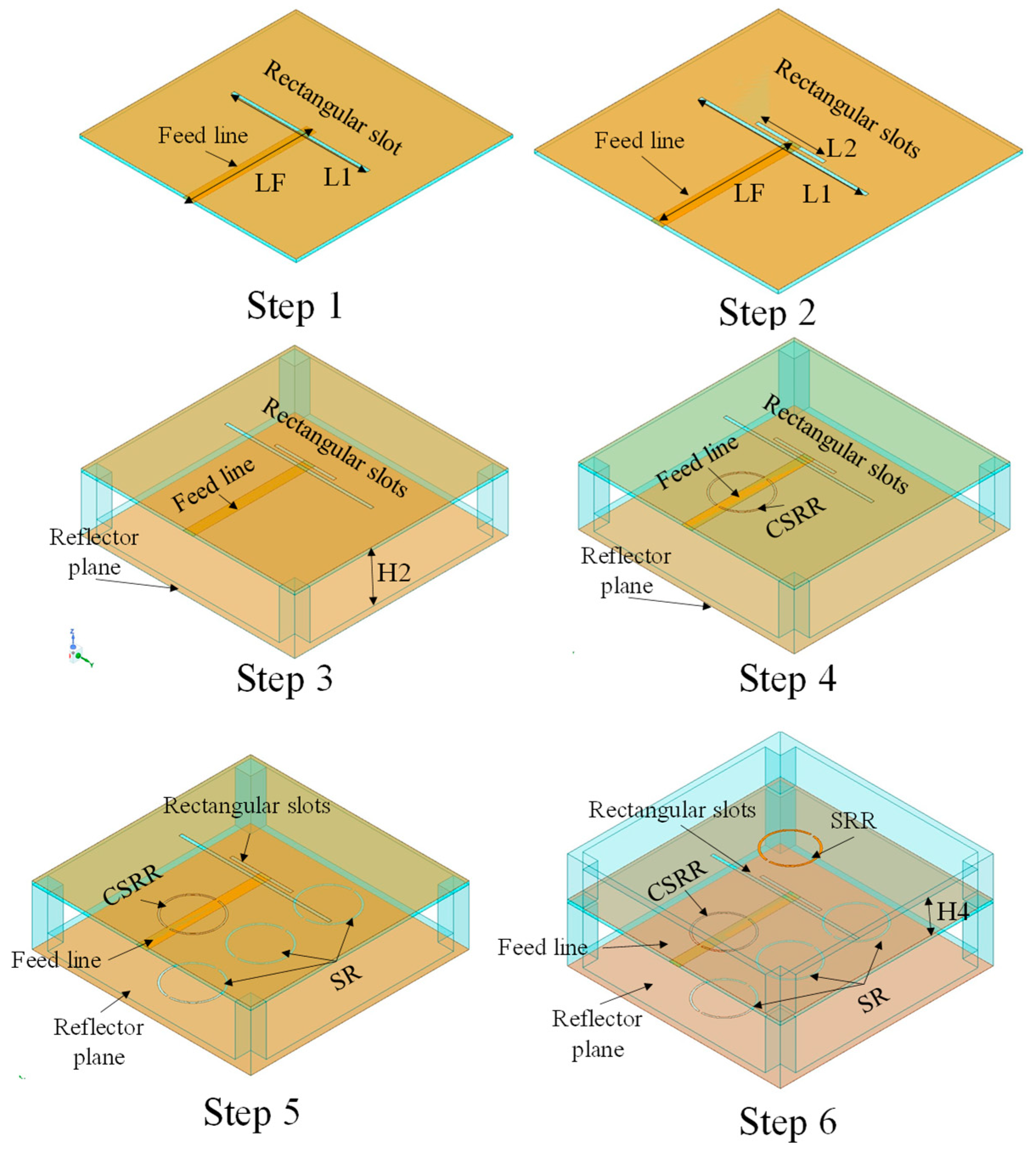
The design evolution process is depicted in
Figure 1. During the first step, the overall effect of the variation of the feed length (LF) and the length of the rectangular slot (L1) were analyzed. Then, the length of the second slot (L2) and the distance of the reflector plane position were varied, which gave rise to an unavoidable resonant frequency shift.
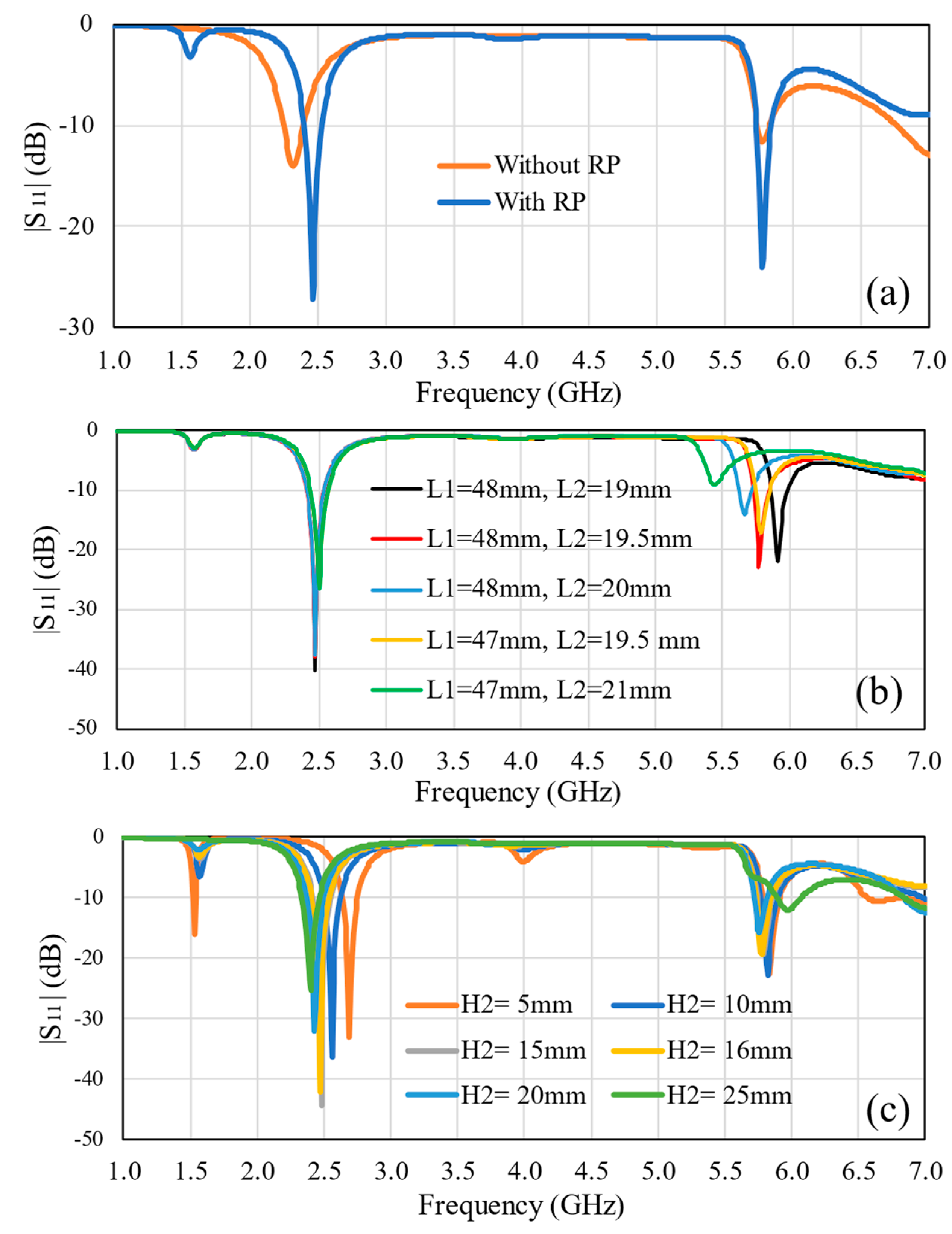
This shift is shown in
Figure 2a, without the RP and with the RP. The variation of LF does not introduce a significant difference, however a smaller reflection coefficient when the RP is used. Additionally,
Figure 2b depicts the reflection coefficient obtained from the variation of slots lengths with a reflector plane (RP) with H2 = 16 mm, and
Figure 2c shows the results from the variation of H2 with L1 = 40 mm and L2 = 19.5 mm.
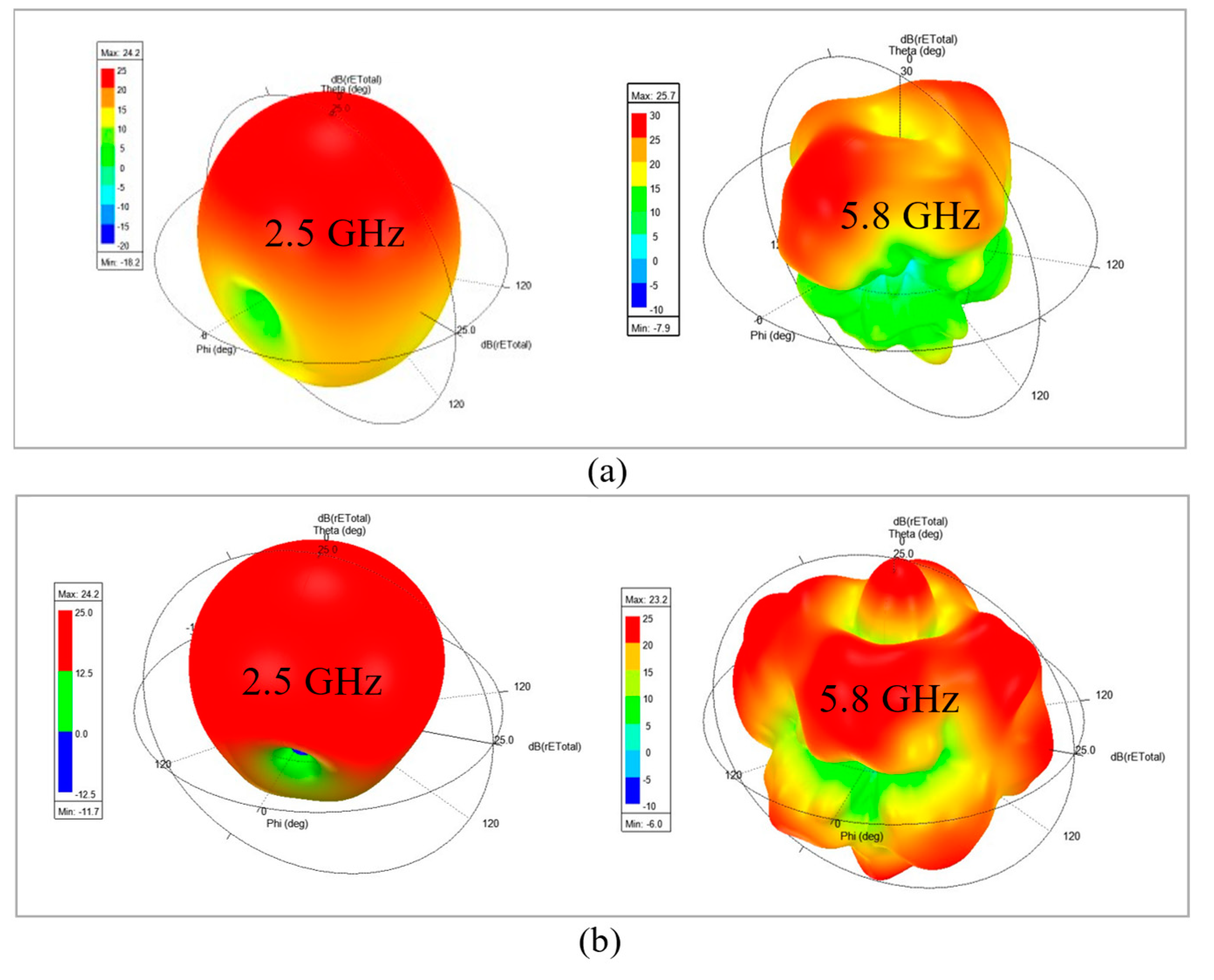
The effect of the reflector plane enhances the reflection coefficient and modifies the radiation pattern shape, increasing the gain values around θ = 0°, such as is shown in
Figure 3a,b. To choose H2, the return losses at the input port and the shape of radiation pattern should be taken into account.
Figure 4 depicts the 3D-radiation pattern at 2.4 GHz and 5.8 GHz. When H2 is 5 mm, this presents a null at θ = 0° in the second band of operation, and when H2 is increased, the null is almost eliminated. However, when H2 is larger, the reflection coefficient is increased, reducing the coupling in the input port. Therefore, H2 is chosen to be 16 mm due to the good values of reflection coefficient, gain, and pattern shape.
The upper SRR in step 6 is mainly used to change the shape of the radiation pattern and enhance the gain values in the second band of operation.
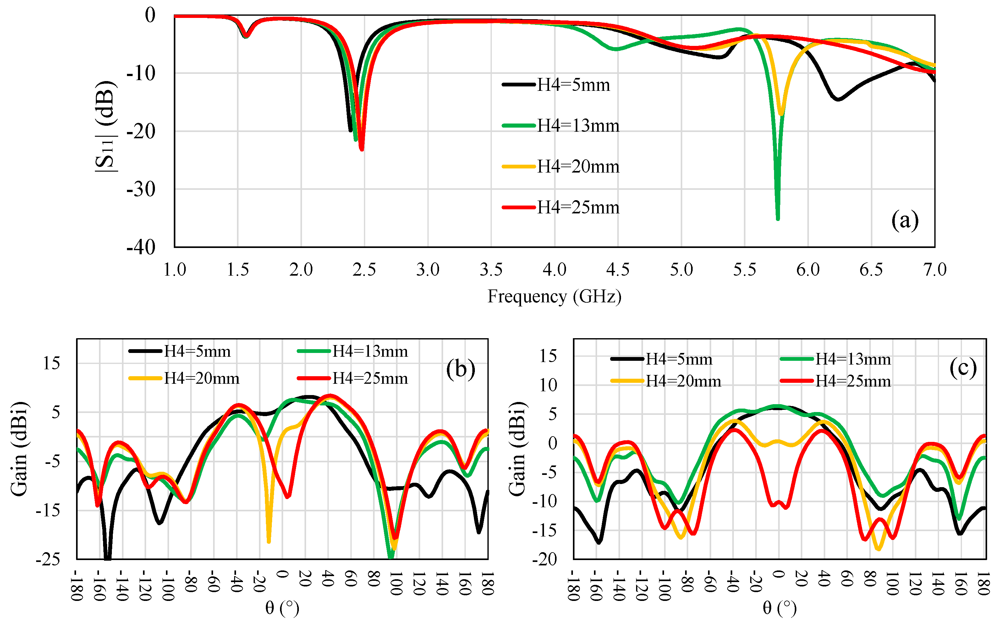
The SRR is excited by proximity to the radiating rectangular slots; then, if H4 changes, the interaction between the slots and SRR change, then the reflection coefficient also changes.
Regarding the radiation pattern, if H4 is large, the SRR is decoupled, and the null is presented around θ = 0°. Otherwise, when H4 is from 5 mm to 15 mm, the null around θ = 0° is eliminated. However, if this height is between 10 and 20 mm, one null appears around θ = 18°, as shown in
Figure 5b,c. H4 is chosen to be 13 mm due to the best values of the reflection coefficient and the elimination of the null at θ = 0° in the second band of operation.
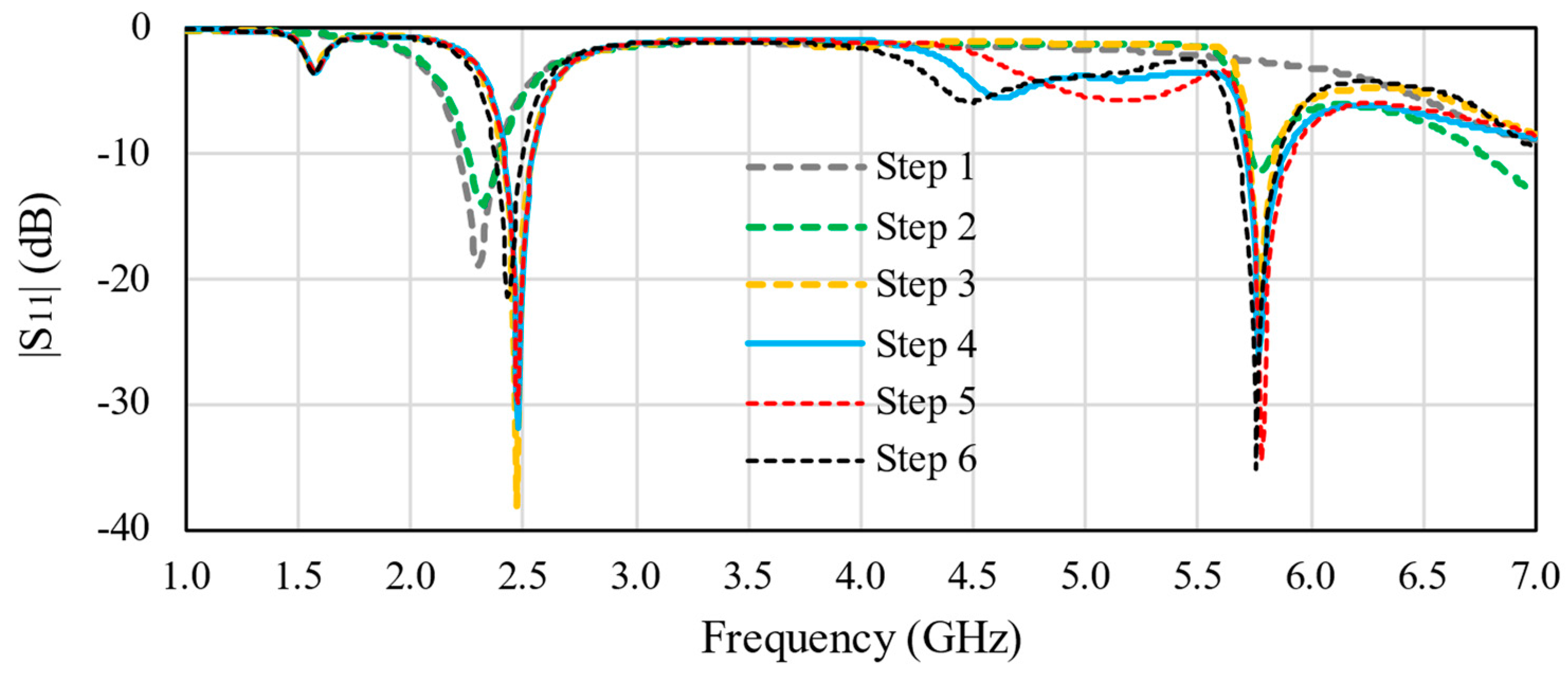
The reflection coefficient from step 1 to step 6 is displayed in
Figure 6; this shows that the Complementary Split Ring Resonator (step 4) and the three-complementary Split Rings (step 5) positioned at the reflector plane contribute to enhance the reflection coefficient in the second band of operation without affecting the first one.
Figure 7 depicts the proposed dual-band antenna in different views, and
Table 1 lists its design parameters.
2.2. Antenna Configuration and Operation Mechanism
The proposed dual-band antenna is based on two rectangular slots positioned over a microstrip line, a complementary split ring resonator (CSRR) atop the feed line, three non-resonant split rings (SR) on the reflector plane, and one split ring resonator (SRR) on top.
The rectangular slots are the principal radiating mechanism in the proposed antenna; the reflector plane is used to increase the gain and modify the radiation pattern; the SRs and CSRR are used to enhance the reflection coefficient in the second band of operation; and the upper SRR is used to change the shape of the radiation pattern around 5.8 GHz, that is, the null at θ = 0° is eliminated when the upper SRR is positioned above the rectangular slots.
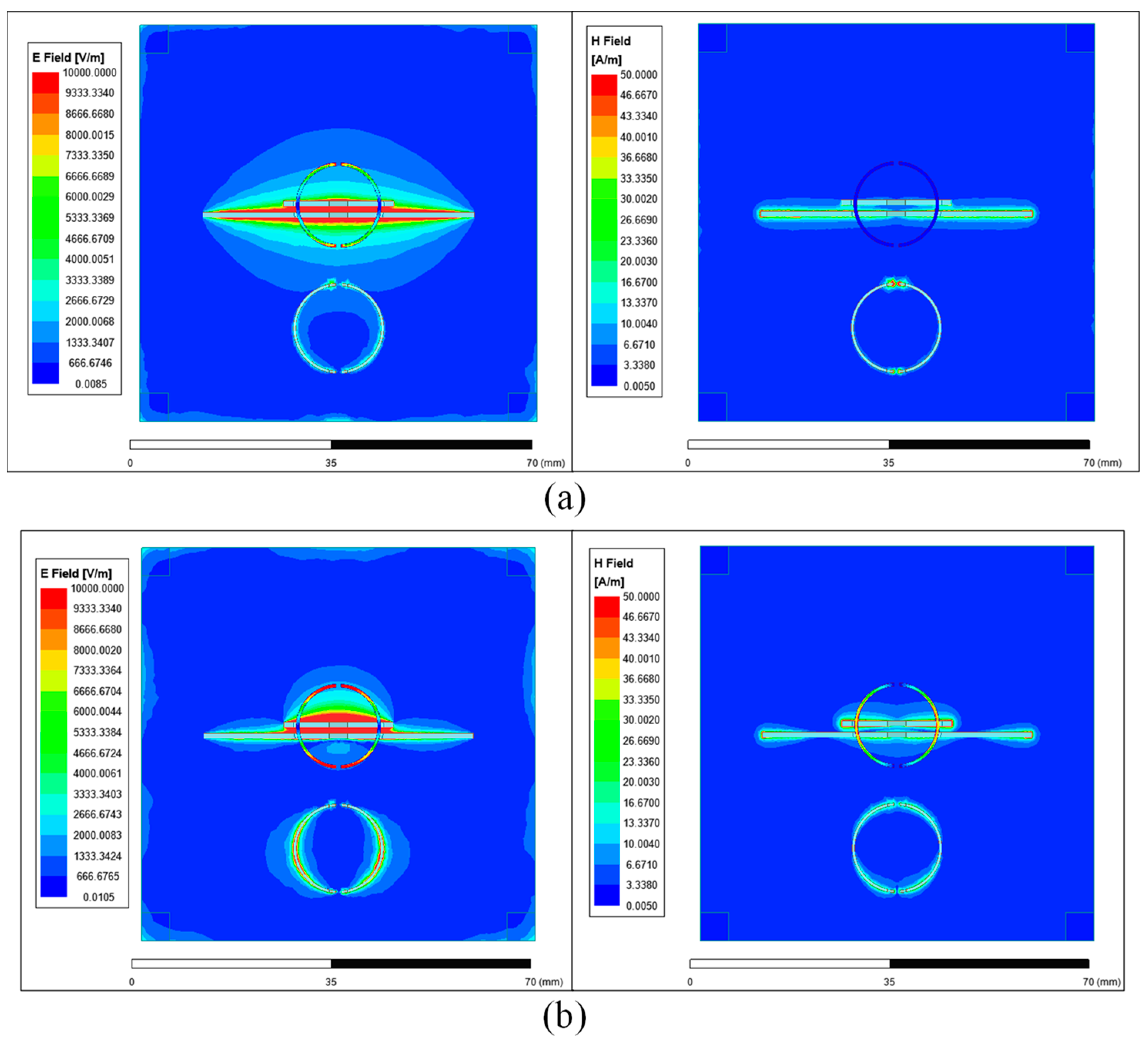
The magnitude of the electric and magnetic fields evaluated in the middle copper layer and in the upper SRR at 2.5 and 5.8 GHz are plotted in
Figure 8, which allow the verification of the resonant mechanism described for the structure, i.e., the rectangular slots are the principal radiating source, and the CSRR is excited by the lower feed line, which acts as a parasitic LC resonator improving the reflection coefficient.
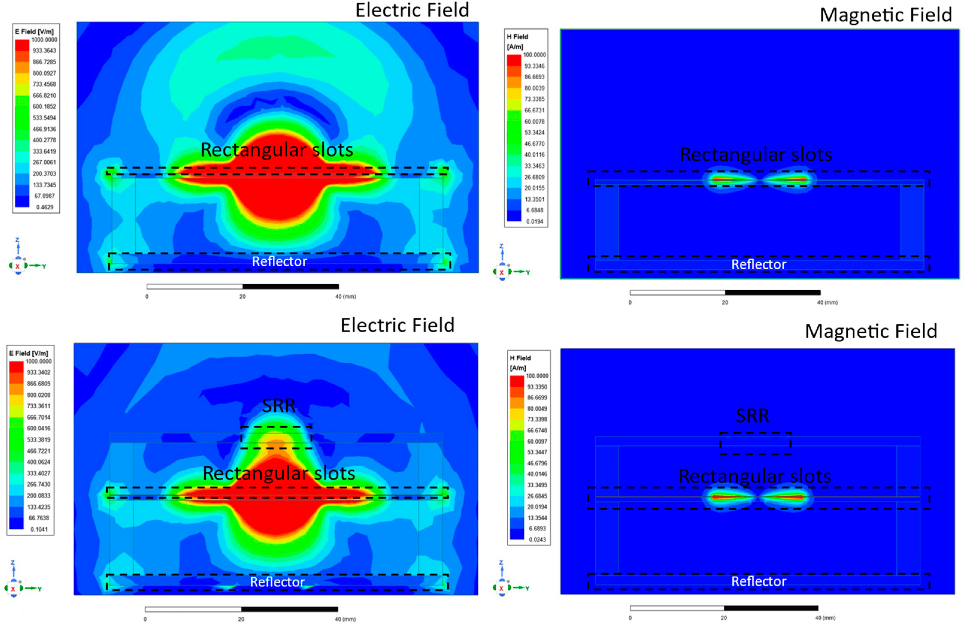
The upper SRR is excited by proximity through the rectangular slots, causing its resonance in the two bands, but the resonance at 5.8 GHz is stronger than in the first one due to the dimensions. The null in θ = 0° is eliminated (for certain values of H4) since the upper SRR “catches” the field lines during their resonance before they reach the RP, acting as a director.
Figure 9 shows the comparison of the electromagnetic fields plotted in the cross-section of the proposed antenna at 5.8 GHz for two cases: when the upper SRR is not used and when it is used. This figure shows that the SRR acts as a director structure, modifying the electric field distribution radiated by the rectangular slot antenna.
Using the analysis of the proposed geometry, a relationship between the elements of the geometry and the resonant length of the principal sources of radiation, that is, the rectangular slots, has been established and is shown in Equations (1) and (2):
where
is the wavelength at the operation frequency,
is the microstrip feed line termination,
the reflector plane effect,
accounts for the influence of the neighboring rectangular slot, and
is the SRR effect. The reflector plane does not have a considerable impact on
because it is relatively far away from it.
Other elements, such as the CSRR and the 3-SRs on the reflector plane, do not have an important impact in the resonant length but have an appreciable one on the return loss.
3. Results
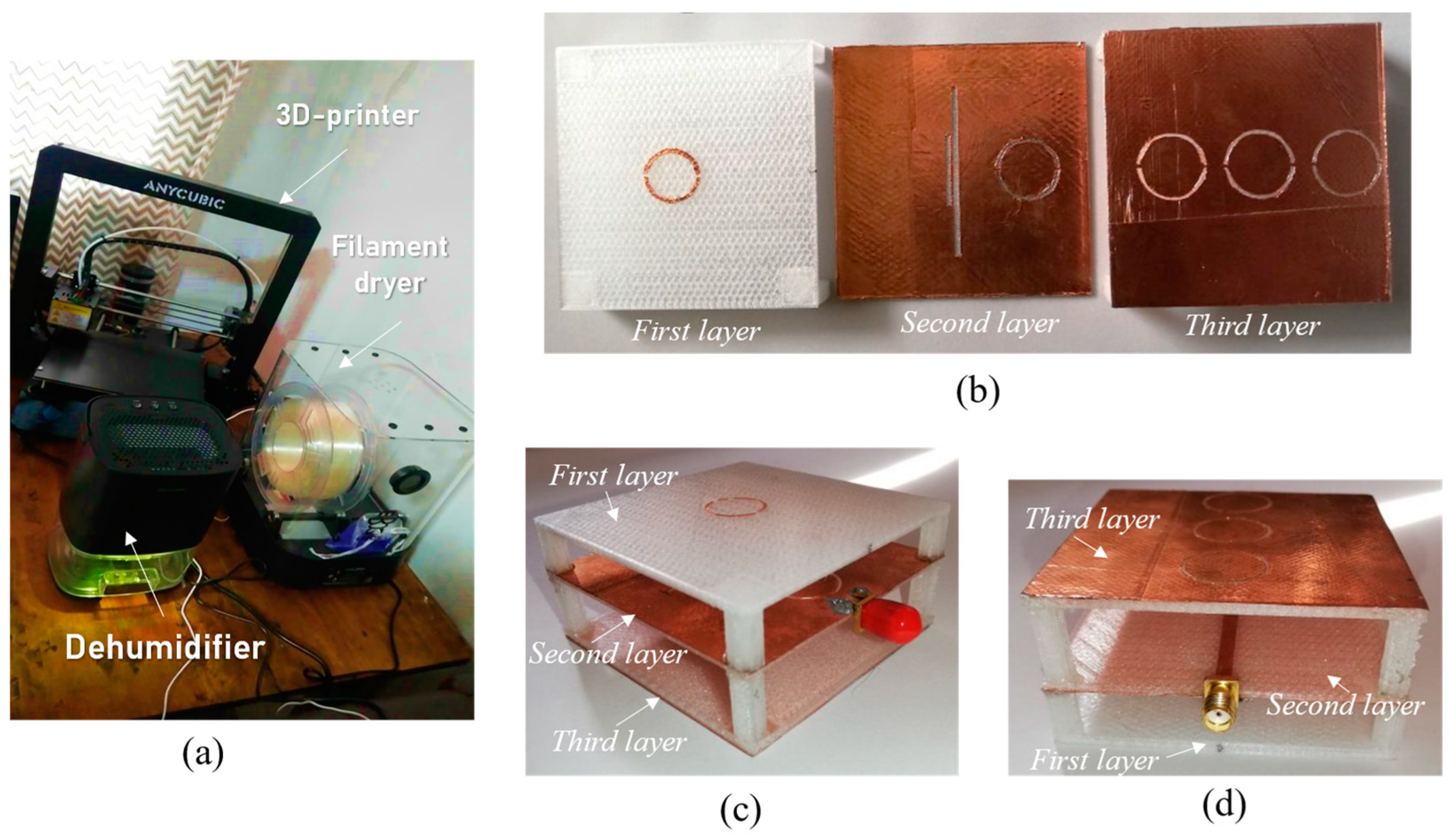
This section demonstrates that the proposed design has significant potential for 2.4/5.8 GHz ISM band applications. The antenna was manufactured using an Any Cubic I3 Mega Pro3D printer, an H2102 dehumidifier, an EIBOS filament, copper adhesive tape, scissors, a precision cutter, and glue, shown in
Figure 10a.
Figure 10b–d shows a fabricated prototype in three different views.
The experiments were conducted using a Vector Network Analyzer (VNA) and a SOLT calibration Kit in an anechoic chamber, and two dual-band antennas to measure the gain using the method proposed in [
22]. In this method, the two antennas are considered identical, and the transmission scattering parameters are measured (S
21) with a separation (S) between antennas higher than the far-field (Ff) condition at the lower frequency of interest. The far-field can be determined using the Equation (3) from [
22].
where
is the is the longest dimension of the antenna and
is the wavelength.
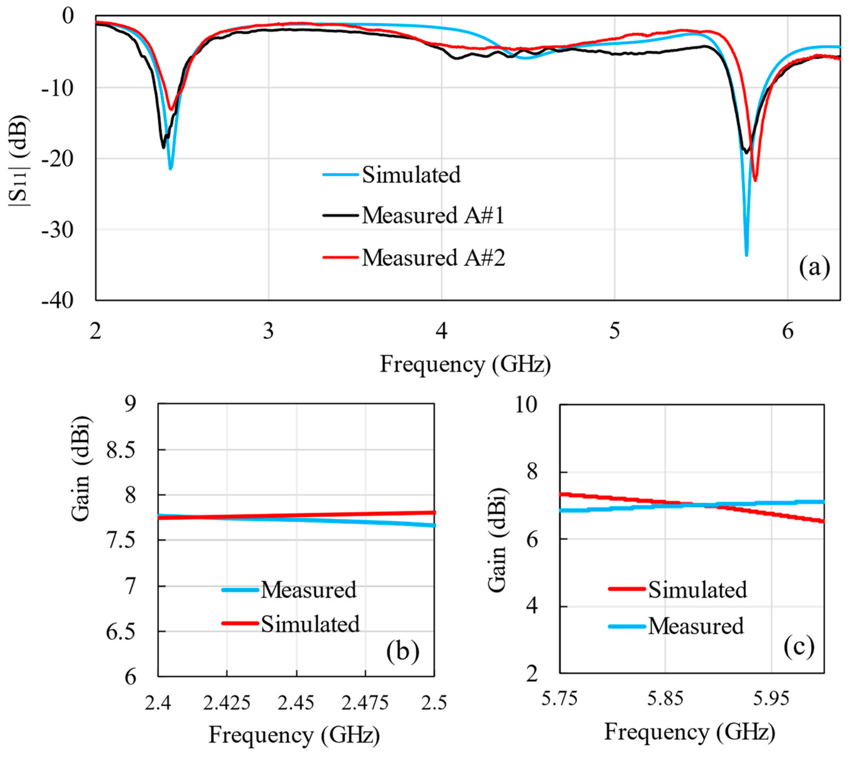
Figure 11a shows the return loss of the proposed dual-band antenna from simulation and measurement considering a reference impedance of 50 Ω covering the 2.4 GHz and 5.8 GHz ISM bands. The figure displays the measured return losses of two prototypes, named A#1 and A#2, showing good correlation with the simulated results.
The measured gain at θ = 0° from 2.4 to 2.5 GHz and from 5.75 to 6 GHz is shown in
Figure 11b,c; it is noteworthy that the simulation and measurement values are almost the same in the whole range. The small differences can be associated either to discrepancies between the electric properties considered in the simulation and real properties of the materials or manufacturing details, such as are the electric conductivity of the glue or even the variations in humidity and temperature.
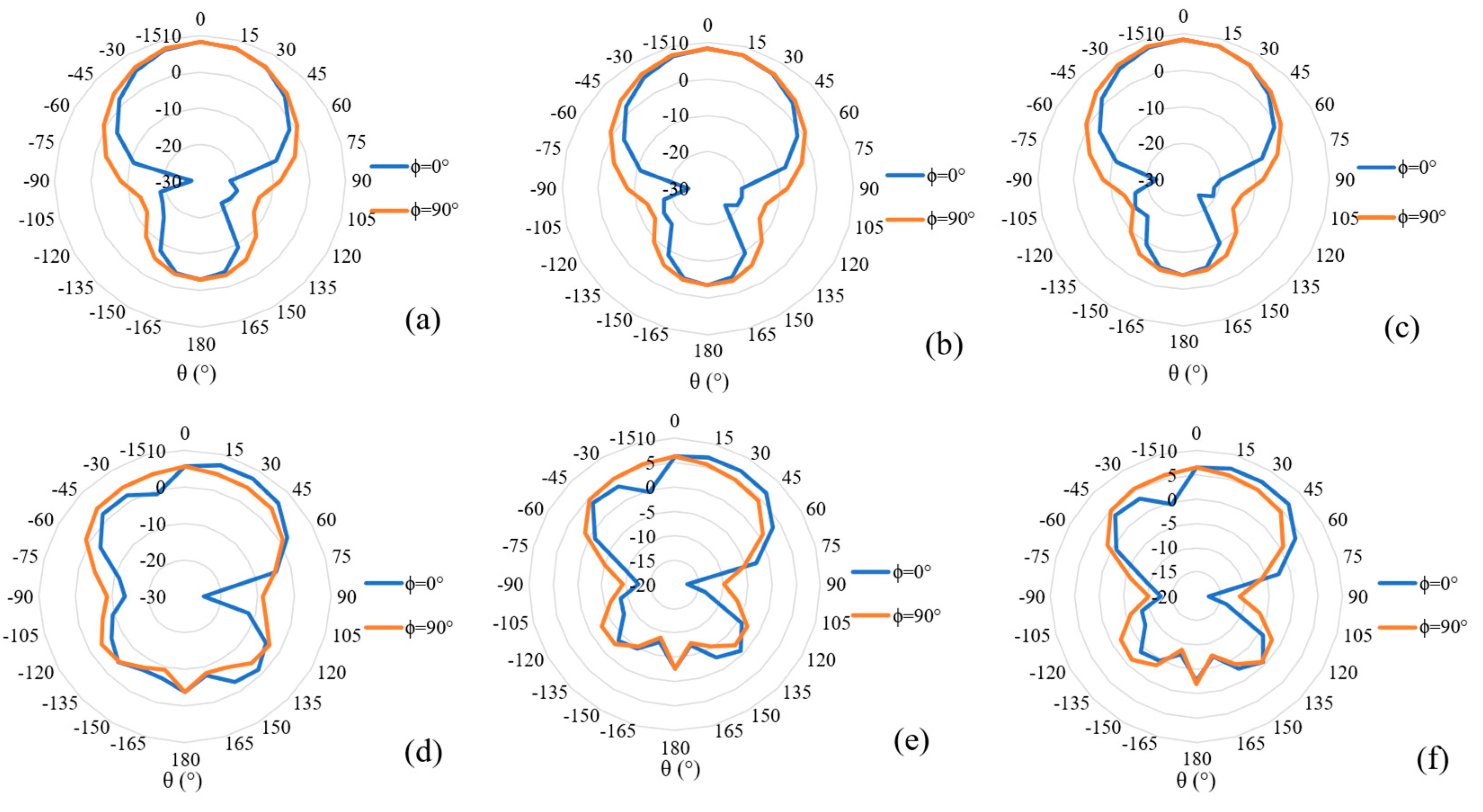
The 2D-radiation patterns from the simulation of three points of the first and second operation bands are shown in
Figure 12a–f. These show a directional and stable behavior across the two impedance bandwidths of operation and with only one principal beam.
The radiation efficiencies obtained from the full-wave simulator are above 90% and 80%, in the first and second band of operation, respectively, considering the loss tangent of the substrate and the finite conductivity of copper.
4. Discussion
Herein, we have presented a dual-band antenna built over a 3D-printed substrate and copper adhesive tape for the metallic layers. The proposed design is based on stacked resonant elements; the main resonant elements are two rectangular slot antennas excited by proximity from a microstrip line, which was designed to be fed by an SMA connector. The second important resonant element is the upper SRR. It has the goal of enhancing the shape of the radiation pattern in the second band of operation.
The reflector plane has three non-resonant split rings acting as a degenerate ground structure (DGS), improving the gain and reflection coefficient.
The proposed design shows good performance, low cost, ease of manufacturing, and it is environmentally friendly since it is built with a biodegradable Polylactic Acid (PLA) substrate.
A comparison between the proposed antenna design and recent published works is provided in
Table 2. The performance of the proposed antenna is remarkably good, with a very inexpensive substrate, a simple and environmentally friendly manufacturing process that uses a biodegradable substrate (PLA-printed substrate) [
23], and with no need for a lithographic process due to the use of copper adhesive tape.
In contrast with [
24,
26,
29,
31], the dual-band antenna proposed in this paper does not require additional substrates for its fabrication, making it of low cost and simple manufacture. The designs from [
25,
27,
28] do not require additional substrates since they are built on PCB, but the gain values are lower than the values obtained with the structure presented here.
The performance of the antenna of [
30] is remarkably good, but it is five times larger than the one we have designed, implying a trade-off between size and performance.
Regarding the total size of the proposed design, this can be considered a moderate size considering that the wavelength at 2.4 GHz is close to 12 cm.
The proposed dual band antenna has a good performance and can be used in devices without size limitations.
5. Conclusions
A dual-band antenna based on two radiating rectangular slots working at 2.45 GHz and 5.8 GHz, respectively, and one upper SRR to enhance the radiation pattern at 5.8 GHz is proposed in this work. The CSSR and SSR are used to enhance the input reflection coefficient. The antenna is designed to be manufactured with a very low-cost PLA-printed substrate and copper adhesive tape, eliminating the lithographic process used for PCB. The dual-band antenna performs well from 2.39 GHz to 2.52 GHz, and from 5.76 GHz to 5.95 GHz, covering the 2.45 GHz and 5.8 GHz ISM bands. The gain is higher than 7.5 dBi and 6.5 dBi, and the simulated radiation efficiency is close to 90% and 80% in the first and second bands, respectively. The theorical values were computed using a full-wave simulator considering finite conductivity of each metal layer and the loss coefficient of PLA substrate. The proposed antenna was fabricated, and the experimental results show a very good correlation with the simulated ones. The total size is 70 × 70 × 31 mm3. The performance of the proposed antenna is good and suitable for devices where the size is not a severe limitation, such as sensors, LPWAN/WLA modules, health care devices, base stations, and control applications and the like.
Author Contributions
K.N.O.-N. conceived the idea, designed the structure, and wrote the principal ideas; R.S.M.-A. revised and edited the manuscript, contributed some ideas, and supervised the work. All authors have read and agreed to the published version of the manuscript.
Funding
This research was funded by Mexican National Council for Science and Technology (CONACyT) under the grants 852217 and 285199.
Data Availability Statement
The datasets used and/or analyzed during the current study are available from the corresponding author on reasonable request.
Acknowledgments
The authors would like to express their gratitude towards Instituto Nacional de Astrofísica, Óptica y Electrónica (INAOE) and CONACyT.
Conflicts of Interest
The authors declare no conflict of interest.
References
- Li, Y.; Luk, M. A Low-Cost 3-D Printed THz Open Resonator Antenna. IEEE Antennas Wirel. Propag. Lett. 2023, 22, 84–88. [Google Scholar] [CrossRef]
- Zhu, J.; Yang, Y.; Hou, Z.; Liao, S.; Xue, Q. Aperture-Shared All-Metal End-Fire High Gain Parabolic Antenna for Millimeter-Wave Multi-Beam and Sub-6 GHz Communication Applications. IEEE Trans. Antennas Propag. 2023, 71, 2784–2789. [Google Scholar] [CrossRef]
- Wang, J.; Xu, J. Environmental implications of PCB manufacturing in China. In Proceedings of the IEEE International Symposium on Electronics and the Environment, Scottsdale, AZ, USA, 10–13 May 2004; pp. 156–158. [Google Scholar] [CrossRef]
- Uzer, D.; Cubuk, S. Three-Dimensional Printed Helical Antenna Compatible with Rotary Wing Unmanned Aerial Vehicles. In Proceedings of the 2022 IEEE Conference on Antenna Measurements and Applications (CAMA), Guangzhou, China, 14–17 December 2022; pp. 1–3. [Google Scholar] [CrossRef]
- Helena, D.; Ramos, A.; Varum, T.; Matos, J. Antenna Design Using Modern Additive Manufacturing Technology: A Review. IEEE Access 2020, 8, 177064–177083. [Google Scholar] [CrossRef]
- Khosravani, M.; Reinicke, T. On the environmental impacts of 3D printing technology. Appl. Mater. Today 2020, 20, 100689. [Google Scholar] [CrossRef]
- Sun, F.; Li, Y.; Wang, J.; Ma, Y.; Ge, L.; Ai, B.; He, R. A Millimeter-Wave Wideband Dual-Polarized Antenna Array With 3-D-Printed Air-Filled Differential Feeding Cavities. IEEE Trans. Antennas Propag. 2022, 70, 1020–1032. [Google Scholar] [CrossRef]
- Shahrubudin, N.; Lee, T.; Ramlan, R. An Overview on 3D Printing Technology: Technological, Materials, and Applications. Procedia Manuf. 2019, 35, 1286–1296. [Google Scholar] [CrossRef]
- Morales, H.; Olvera, J.; Corona, A.; Kataria, T. Dielectric Characterization of Anisotropic 3D-Printed Biodegradable Substrates Based on Polylactic Acid. IEEE Microw. Mag. 2021, 22, 18–100. [Google Scholar] [CrossRef]
- Khan, Z.; He, H.; Chen, X.; Virkki, J. Dipole Antennas 3D-printed from Conductive Thermoplastic Filament. In Proceedings of the 2020 IEEE 8th Electronics System-Integration Technology Conference (ESTC), Tønsberg, Norway, 15–18 September 2020; pp. 1–4. [Google Scholar] [CrossRef]
- Dhaliwal, B.; Singla, K.; Saini, G. Analysis of the Effect of Infill Density of 3D Printed Substrate on Rectangular Microstrip Antenna Performance. In Proceedings of the 2021 IEEE Indian Conference on Antennas and Propagation (InCAP), Jaipur, India, 13–16 December 2021; pp. 984–987. [Google Scholar] [CrossRef]
- Karki, S.; Ala-Laurinaho, J.; Viikari, V. Dual-Polarized Probe for Planar Near-Field Measurement. IEEE Antennas Wirel. Propag. Lett. 2022, 22, 576–580. [Google Scholar] [CrossRef]
- Li, M.; Yang, Y. Single- and Multiple-Material Additively Manufactured Electronics: A Further Step from the Microwave-to-Terahertz Regimes. IEEE Microw. Mag. 2023, 24, 30–45. [Google Scholar] [CrossRef]
- He, X.; Tentzeris, M. A 3D Printed Dish Antenna with Integrated Feeding Structure. In Proceedings of the 2020 IEEE International Symposium on Antennas and Propagation and North American Radio Science Meeting, Montreal, QC, Canada, 5–10 July 2020; pp. 1603–1604. [Google Scholar] [CrossRef]
- Czelen, M.; Rzymowski, M.; Nyka, K.; Kulas, L. Miniaturization of ESPAR Antenna Using Low-Cost 3D Printing Process. In Proceedings of the 2020 14th European Conference on Antennas and Propagation (EuCAP), Copenhagen, Denmark, 15–20 March 2020; pp. 1–4. [Google Scholar] [CrossRef]
- Qu, Z.; Zhou, Y.; Alkaraki, S.; Kelly, J.; Gao, Y. Continuous Beam Steering Realized by Tunable Ground in a Patch Antenna. IEEE Access 2023, 11, 4095–4104. [Google Scholar] [CrossRef]
- Yuan, Y.; Chen, S.; Fumeaux, C. A 3D-Printed Hybrid Dielectric Resonator Antenna with Low Cross-Polarization. In Proceedings of the 2022 International Symposium on Antennas and Propagation (ISAP), Sydney, Australia, 31 October–3 November 2022; pp. 79–80. [Google Scholar] [CrossRef]
- Shrestha, S.; Abbas, S.; Asadnia, M.; Esselle, K. Realization of Three-Dimensional Printed Multi-Layer Wide Band Prototype. IEEE Access 2022, 10, 130944–130954. [Google Scholar] [CrossRef]
- Trzebiatowski, K.; Kalista, W.; Rzymowski, M.; Kulas, Ł.; Nyka, K. Multibeam Antenna for Ka-Band CubeSat Connectivity Using 3-D Printed Lens and Antenna Array. IEEE Antennas Wirel. Propag. Lett. 2022, 21, 2244–2248. [Google Scholar] [CrossRef]
- Bharambe, V.; Ma, J.; Dickey, M.; Adams, J. Planar, Multifunctional 3D Printed Antennas Using Liquid Metal Parasitics. IEEE Access 2019, 7, 134245–134255. [Google Scholar] [CrossRef]
- Olan, K.; Murphy, R.; Alibakhshikenari, M. Dual-band Slot-SSR Antenna on PLA-printed Substrate for 2.4/5.8 GHz ISM-Band Internet of Things (IoT) Applications. In Proceedings of the IEEE 8th World Forum on Internet of Things, Yokohama, Japan, 26 October–11 November 2022. [Google Scholar]
- Medina, J.; Diaz, E.; Olvera, J.; Chavez, R.; Velázquez, A. Análisis y Comparación de Metodologías Para Determinar Experimentalmente la Ganancia de Antenas de RF y Microondas. In Proceedings of the Simposio de Metrología 2008, Santiago de Querétaro, Mexico, 22–24 October 2008; Available online: https://www.cenam.mx/simposio2008/sm_2008/memorias/m1/sm2008-m127-1150.pdf (accessed on 3 April 2023).
- Singhvi, M.; Zinjarde, S.; Gokhale, D. Polylactic acid: Synthesis and biomedical applications. J. Appl. Microbiol. 2019, 127, 1612–1626. [Google Scholar] [CrossRef] [PubMed]
- Dalal, P.; Rafique, U.; Abbas, S.; Pradhan, N.; Kathikeyan, S. Dual-band wearable antenna for wireless body area networks on a flexible substrate. In Proceedings of the 2022 IEEE Wireless Antenna and Microwave Symposium (WAMS), Rourkela, India, 5–8 June 2022; pp. 1–5. [Google Scholar] [CrossRef]
- Wang, C.; Cao, X.; Cai, Q.; Zhu, Y. Design of a Dual-Band Slot Loop Antenna for Wi-Fi Application Based on Characteristic Mode Analysis. In Proceedings of the 2022 IEEE International Symposium on Antennas and Propagation and USNC-URSI Radio Science Meeting (AP-S/URSI), Denver, CO, USA, 10–15 July 2022; pp. 187–188. [Google Scholar] [CrossRef]
- Gao, G.; Dou, Z.; Yu, Z.; Zhang, B.; Dong, J.; Hu, B. Dual-Mode Patch Antenna with Capacitive Coupling Structure for On-/Off-Body Applications. IEEE Antennas Wirel. Propag. Lett. 2022, 21, 1512–1516. [Google Scholar] [CrossRef]
- Iqbal, A.; Mabrouk, I.; Hasan, M.; Nedil, M.; Denidni, T. Wideband Substrate Integrated Waveguide Antenna for Full-Duplex Systems. IEEE Antennas Wirel. Propag. Lett. 2022, 21, 212–216. [Google Scholar] [CrossRef]
- Fan, J.; Lin, J.; Cai, J.; Qin, F. Ultra-wideband circularly polarized cavity-backed crossed-dipole antenna. Sci. Rep. 2022, 12, 4569. [Google Scholar] [CrossRef] [PubMed]
- Montisci, G.; Mura, G.; Muntoni, G.; Casula, G.; Chietera, F.; Aburish, M. A Curved Microstrip Patch Antenna Designed from Transparent Conductive Films. IEEE Access 2023, 11, 839–848. [Google Scholar] [CrossRef]
- Hijazi, H.; Le, M.; Lababidi, R.; Le, D.; Pérennec, A. 3D-Printed Ultra-Wideband In-Band Full-Duplex Antenna System with Grating Lobes Reduction. In Proceedings of the 2022 International Conference on Microelectronics (ICM), Casablanca, Morocco, 4–7 December 2022; pp. 86–89. [Google Scholar] [CrossRef]
- Kalista, W.; Leszkowska, L.; Rzymowski, M.; Nyka, K.; Kulas, L. Low-Cost 3D Printed Dielectric Lens Antennas for 5.9 GHz Frequency Band V2X Applications. In Proceedings of the 2022 24th International Microwave and Radar Conference (MIKON), Gdansk, Poland, 12–14 September 2022; pp. 1–4. [Google Scholar] [CrossRef]
Figure 1.
Design evolution process.
Figure 1.
Design evolution process.
Figure 2.
Reflection coefficient at the input port for (a) two slots with and without RP, (b) variation of L1 and L2, and (c) H2 variation.
Figure 2.
Reflection coefficient at the input port for (a) two slots with and without RP, (b) variation of L1 and L2, and (c) H2 variation.
Figure 3.
Two-dimensional-gain pattern between step 2 and step 3 at (a) 2.5 GHz and (b) 5.8 GHz.
Figure 3.
Two-dimensional-gain pattern between step 2 and step 3 at (a) 2.5 GHz and (b) 5.8 GHz.
Figure 4.
Three-dimensional-radiation patterns when (a) H2 = 5 mm and (b) H2 = 25 mm.
Figure 4.
Three-dimensional-radiation patterns when (a) H2 = 5 mm and (b) H2 = 25 mm.
Figure 5.
Evaluation of distance between SRR and rectangular slots (H4) in (a) return losses and gain pattern at 5.8 GHz at (b) φ = 0° and (c) φ = 90°.
Figure 5.
Evaluation of distance between SRR and rectangular slots (H4) in (a) return losses and gain pattern at 5.8 GHz at (b) φ = 0° and (c) φ = 90°.
Figure 6.
Reflection coefficient at the input port from the design process evolution from
Figure 1.
Figure 6.
Reflection coefficient at the input port from the design process evolution from
Figure 1.
Figure 7.
Proposed dual-band antenna on 3D-printed substrate.
Figure 7.
Proposed dual-band antenna on 3D-printed substrate.
Figure 8.
Electric and magnetic fields in magnitude (a) at 2.5 GHz and (b) at 5.8 GHz.
Figure 8.
Electric and magnetic fields in magnitude (a) at 2.5 GHz and (b) at 5.8 GHz.
Figure 9.
Electric and magnetic fields in magnitude plotted on the cross-section (YZ plane) of the proposed antenna at 5.8 GHz: without SRR (above) and with SRR (below).
Figure 9.
Electric and magnetic fields in magnitude plotted on the cross-section (YZ plane) of the proposed antenna at 5.8 GHz: without SRR (above) and with SRR (below).
Figure 10.
(a) Manufacturing equipment and fabricated antenna using PLA 3D-printed substrate and copper adhesive tape, (b) top view of separated layers, (c) bird’s eye view (top), and (d) side view showing the bottom layer.
Figure 10.
(a) Manufacturing equipment and fabricated antenna using PLA 3D-printed substrate and copper adhesive tape, (b) top view of separated layers, (c) bird’s eye view (top), and (d) side view showing the bottom layer.
Figure 11.
Results from simulation and measurement of the (a) reflection coefficient, and gain (θ = 0°) at the (b) 2.4 GHz band and (c) 5.8 GHz band.
Figure 11.
Results from simulation and measurement of the (a) reflection coefficient, and gain (θ = 0°) at the (b) 2.4 GHz band and (c) 5.8 GHz band.
Figure 12.
Two-dimensional-radiation patterns at (a) 2.4 GHz, (b) 2.45 GHz, (c) 2.5 GHz, (d) 5.75 GHz, (e) 5.8 GHz, and (f) 5.85 GHz from a full-wave simulator.
Figure 12.
Two-dimensional-radiation patterns at (a) 2.4 GHz, (b) 2.45 GHz, (c) 2.5 GHz, (d) 5.75 GHz, (e) 5.8 GHz, and (f) 5.85 GHz from a full-wave simulator.
Table 1.
Design parameters for the proposed antenna.
Table 1.
Design parameters for the proposed antenna.
| Parameter | Value (mm) | Parameter | Value (mm) | Parameter | Value (mm) |
|---|
| X | 70 | L1 | 48 | LF | 40 |
| H1 | 1 | H3 | 2 | GAP | 1 |
| R1 | 8 | Z | 32 | L2 | 19.5 |
| WF | 3.27 | H2 | 16 | H4 | 13 |
| WR | 1 | R2 | 7.5 | t | 0.025 |
| dx | 0 | Y | 70 | - | - |
Table 2.
Comparison with recent and related works.
Table 2.
Comparison with recent and related works.
| | Work | [24] | [25] | [26] | [27] | [28] | [29] | [30] | [31] | This Work |
|---|
| Parameter | |
|---|
Bands of operation
(GHz) | 2.4
5.8 | 2.4
5.8 | 2.4
5.8 | 4.9
5.8 | 1.67–7.26 | 2.15 | 2–20 | 5.9 | 2.45
5.8 |
| Impedance bandwidth | 1.9 GHz
523 MHz | 840 MHz
1.32 GHz | 90 MHz
330 MHz | 420 MHz
460 MHz | 5.59 GHz | 493/518 MHz | 18 GHz | 250–300 MHz | 130 MHz
190 MHz |
| Gain | N.A. | 4.62 dBi
5.21 dBi | −2.38 dBi
6.67 dBi | 5.24 dBi
5.37 dBi | ≥7.3 dBic | 2.57 dBi | 12.8 dBi (avg) | 14.5 dBi | 7.8 dBi
6.8 dBi |
| Substrate | Flexible polycarbonate &
Rohacell foam | FR4 | Polydimen-
thylsiloxane | RO4003 C | Duroid 5880 | Transparent PETG
(3D-printed) | 3D-printed | RO3003
3D-printed PLA | 3D-printed PLA |
Total size
(mm3) | 225 | 4237 | 4246 | 557 | 11,332 | >112,500 | 765,000 | 458,990 | 151,900 |
| Cost-Complexity | U–Low | Low–Low | U–Moderate | Moderate–Moderate | Moderate–Moderate | U–Moderate | Very low–Low | Low cost–Moderate | Very low–Moderate |
| Disclaimer/Publisher’s Note: The statements, opinions and data contained in all publications are solely those of the individual author(s) and contributor(s) and not of MDPI and/or the editor(s). MDPI and/or the editor(s) disclaim responsibility for any injury to people or property resulting from any ideas, methods, instructions or products referred to in the content. |
© 2023 by the authors. Licensee MDPI, Basel, Switzerland. This article is an open access article distributed under the terms and conditions of the Creative Commons Attribution (CC BY) license (https://creativecommons.org/licenses/by/4.0/).
