Article

GPR-Based Framework for Statistical Analysis of Gate Delay under NBTI and Process Variation Effects

National ASIC System Engineering Research Center, School of Electronic Science and Engineering, Southeast University, Nanjing 210023, China
*
Author to whom correspondence should be addressed.
Electronics 2022, 11(9), 1336; https://doi.org/10.3390/electronics11091336
Submission received: 16 March 2022 / Revised: 17 April 2022 / Accepted: 20 April 2022 / Published: 22 April 2022
(This article belongs to the Section Circuit and Signal Processing)

Abstract

:
With the aggressive scaling of feature size, Negative Bias Temperature Instability (NBTI) and Process Variation (PV) have become major issues for circuit reliability and yield. In this paper, we analyze the variation of gate delay by jointly considering NBTI and PV effects. Using Gaussian Process Regression (GPR) learning interface, a Statistical Gate Delay Extraction (SGDE) framework is proposed. Typical types of logic gates are simulated with commercial 28 nm technology for verifying the performance of SGDE in the experiment. Compared to the golden data, the results show that our proposed approach achieves minimal loss of accuracy with significant runtime speed-up.

1. Introduction

The rapid scaling of CMOS technology has resulted in new reliability concerns, such as Electro Migration (EM), Stress Migration (SM), Negative Bias Temperature Instability (NBTI), Time-Dependent Dielectric Breakdown (TDDB), and Hot Carrier Injection (HCI), etc. [1]. The state-of-the-art research shows that among different aging mechanisms of technologies below 90 nm, NBTI is the most dominant factor, threatening reliability, and degrading performance (down to 80%) [2]. In this paper, we mainly focus on NBTI aging and investigate the effects on the reliability.
NBTI occurs in pMOS and it can be viewed in two stages (i.e., stress and recovery). When the gate of pMOS is under negative bias ( V g s < 0 ), the threshold voltage of the transistor increases, leading to the decrease of drive current ( I D ). Then, the reduction of I D in turn, results in the performance degradation of a circuit, and may eventually cause the breakdown of the whole electrical system. During the recovery phase, when the gate bias is OFF ( V g s = 0 ), | V t h | will decrease and partially recover to its initial value. NBTI degradation increases gradually with the above two phases back and forth [3].
Moreover, the impact of NBTI is exacerbated by Process Variation (PV), which results in a complex analysis of circuit reliability [4]. PV occurs in the processing steps during semiconductor production, causing differences between the intended device parameters in the design stage and the actual device parameters. Most of the prior works treated NBTI and PV as two independent issues and addressed the impact of each effect on IC reliability and performance separately. However, with the scaling of the technology node, considering both effects is an urgent need for tape-out flow [5]. PV, such as oxide thickness ( T o x ) and initial threshold voltage ( V t h 0 ), will affect NBTI potentially.
In this paper, NBTI and PV have become the most prominent effects able to affect the circuit reliability, making greater challenges against the traditional gate delay characterization. Fortunately, Machine Learning (ML) algorithms can capture the underlying correlations between predictor variables. Among many features offered by ML, we are particularly interested in accelerating applications by replacing computationally expensive tasks with fast predictions.
In this article, we present an ML based framework (i.e., SGDE) to evaluate the variation of gate delay by considering the combined effect of NBTI and process variation. The main contributions of this work are as follows:
  • Derive an abstract expression related to gate delay. From the expression, the main factors affecting the variation of gate delay are explicit, and the predictor variables and targets of ML can be determined easily. Using the ML model, we can eliminate the time-consuming SPICE simulations by the traditional process.
  • Apply the ML model to a fast Monte–Carlo simulation. Our goal is not only to predict the individual outcome for a specified set of input features but also to evaluate the distribution of gate delay from numerous outputs. With the ML model, a predicting process can be completed with fast runtime, which enables the designers to evaluate the statistical characteristics of gate delay in a Monte-Carlo fashion.
The sections below will be expanded in this order: Section 2 introduces the background and previous research concerning NBTI degradation and PV. Section 3 illustrates the main idea and main contributions of our research. Section 4 reports the detailed experimental results and comparison with previous work. A summary and outlook are provided in Section 5.

2. Background and Related Work

2.1. NBTI Degradation

Nowadays, the reaction–diffusion (R–D) model is widely used to interpret the NBTI mechanisms [6]. According to the numerical solution of the standard reaction diffusion (R–D) model, The NBTI aging model equations were formed, which built the basic foundation for reliability research.
When a pMOS transistor is suffering a continuous stress period from t 0 to t , the threshold voltage will increase eventually, which can be expressed by Equation (1) [7].
Δ V t h = K v 2 . ( t t o ) 1 / 2 + Δ V t h 1 2 + δ v ,
where
K v = A N B T I × T o x × C o x ( V d d V t h 0 ) × e ( V d d V t h 0 T o x × E 0 E a k × T )
For a detailed parameter description, please refer to reference [7].
In a real situation, the gate voltage of pMOS cannot be constant. However, it will change simultaneously with different workloads. When V g s = 0, the threshold voltage of pMOS will partially recover. Equation about the Δ V t h of a pMOS transistor assuming the recovery happens at t 0 , i.e., dynamic NBTI, is shown below [7].
Δ V t h = ( Δ V t h 1 δ v ) ( 1 η ( t t 0 ) / t )
In order to save computing resources during the long-term NBTI dynamic effect, a closed form of the transient aging model was proposed [8], which includes the recovery effect and is useful for the estimation of degradation by years. In this model, the total V t h degradation after time t has passed ( Δ V t h , t ) is expressed as Equation (4).
Δ V t h , t = ( K v 2 . T c l k . α 1 β t 1 / 2 n ) 2 n
where T c l k and α refers to clock cycle and stress probability, respectively. Here, α is defined as the time ratio of the stress phase in the whole working time, i.e., ( t s t r e s s t s t r e s s + t r e c o v e r y ). β t is a parameter that has a relation with temperature, T c l k , α , and t . When the clock frequency is higher than 10 kHz, there is little relation between Δ V t h , t and T c l k [8]. In this case, the relationship between Δ V t h , t and α can be formulated as Equation (5).
Δ V t h , t ( 0.001 n 2 K v 2 α C t 0.81 T o x 2 ( 1 α ) ) n
To simulate the degradation of NBTI, an accurate aging model card and efficient simulation analysis are urgently needed. In the industry, there are three mainstream aging APIs, namely, MOSRA, RelXpert, and Eldo, which are the products of Synopsys, Cadence, and Mentor Graphics respectively. In this work, we will use MOSRA, which is fully compatible with HSPICE, to model the gate-level degradation behavior if not particularly indicated.

2.2. Process Variations

In general, process variation (PV) is caused by the minor fluctuations of dopant atoms during fabrication, resulting in the variation of the device’s electrical parameters, which can be seen as a stochastic deviation from the device’s nominal behavior [9]. The PVs can be divided into the global and the local ones. Global variations affect all devices and interconnect on a die equally. Local variations have different effects on devices or interconnect inside a die, leading to the deviation between device parameters inside a chip after manufacturing.
In the past, these PVs did not greatly affect circuit performance. As the nodes of technology are scaling down, these variations, however, do not follow the scaling linearly but lag behind the pace. Consequently, the ratio of process variations to the nominal dimensions of devices becomes larger, which will affect the delays of logic gates significantly [10]. In this case, traditional corner-based circuit analysis methods present many limitations in considering the effects of process variations, and the delays of logic gates need to be modeled as random variables instead of fixed values in nanometer manufacturing nodes [10].
In these PVs, T o x together with V t h 0 has become an integral part of the degradation of reliability, specifically while catering to the NBTI mechanism [11]. In many cases, these critical process variations are assumed to satisfy the Gaussian distribution, which will determine the statistical characteristics of gate delay.

2.3. Explicit Analytical Model

With the increase in reliability challenges, researchers have focused on analyzing the variations of gate delay. Several works have been available in the literature to consider the NBTI and PV issues jointly, which can be classified into the following categories.

2.3.1. Explicit Analytical Model

Yinghai Lu et al. in [5] proposed a nonlinear scalable statistical gate delay model, which considers both run-time gate working conditions and fabrication-induced process variation. In this paper, a set of process parameters, such as V t h 0 , T o x , the channel width ( W e f f ) and the channel length ( L e f f ) are considered as random variables conformed with Gaussian normal distribution. They use the polynomial chaos expansion on the set of random variables to characterize the variation of gate delay degradation. The aging effects of each gate, including the means and the variances, are compared against the results of the corresponding 5000-point Monte-Carlo simulation.
In [12], the effects of the variation of the major process parameters ( T o x and V t h 0 ) on NBTI were analyzed. By the means of strict derivation, the probability density functions (PDFs) of the electric field generated on the gate oxidized layer ( E o x ) and Δ V t h were obtained. Then, an analytical model of the degraded gate delay was proposed, from which the corresponding mean and the standard deviation can also be deduced. In the experiment, the compact gate delay model was verified by a 10,000-point Monte-Carlo simulation.
In [5,12], the relative gate delay change is approximated as a linear function of Δ V t h , where the analytical model only involves one Δ V t h , ignoring the possible Δ V t h occurring on other pMOS transistors. For a multi-input cell, such as a 2-input NOR gate, whether the designated input port has a rising or falling arc, the other port may maintain a low voltage level, which will affect the degradation of gate delay potentially. Ignoring this consideration, an optimistic analysis will be obtained.

2.3.2. Implicit Analytical Model

To capture the dependence of the gate output delay on the Δ V t h and other PV effects, [4] also proposed a gate delay model. Different from the literature [5,12], the gate delay model in [4] does not explicitly express the relationship with PVs, but is implicitly expressed by two fitting parameters. The fitting parameters can be extracted by intensive SPICE simulations of individual gates under various PV parameters ( L e f f , W e f f   V t h 0 , T o x , and μ 0 ).
In [4], all pMOS transistors are assumed to be degraded at the same rate. Obviously, it will lead to a pessimistic result because some transistors may not produce Δ V t h .
Obviously, previous research works mainly focused on the analytical model. Nevertheless, an approach that can evaluate the statistical characteristics of gate delay by a low-runtime and high-accuracy method has not yet evolved. Our main work is to suggest a GPR-based framework to obtain the statistical result of gate delay by jointly considering the NBTI and PV effects. In addition to PVs, the predictor variables of the ML model include all the Δ V t h occurring on any pMOS transistor in a gate, which can avoid the pessimistic or optimistic analysis.

3. SGDE: GPR-Based Framework for Statistical Analysis of Gate Delay under NBTI and Process Variation Effects

3.1. The Effect of PV on NBTI

NBTI actually depends on several process parameters including V t h 0 , T o x , etc., so that process variations actually interfere with the aging statistical impact [13]. In [4,5,12], several process parameters are included for estimating the gate aging effects. These works claim that circuit aging by NBTI could severely be affected by the magnitude of the process variations.
The main purpose of this chapter is to analyze the effect of PV on NBTI. Taking the INV gate as an example, it is to study the influence of PV on the Δ V t h of pMOS transistor in the gate. The INV gate is modeled using commercial 28 nm technology, where V t h 0 , T o x , channel length offset due to mask/etch effect (XL) and channel width offset due to mask/etch effect (XW) are characterized as Gaussian random variables. The variance of each random parameter is set as 5% of its mean. Table 1 lists their nominal and standard deviation values. The supply voltage, working temperature, and stress time are set as 0.9 V, 100 °C and 10 years, respectively. To maximize the NBTI effect, continuous low voltage stress is supplied to INV.
Firstly, we analyze the distribution of V t h during two different conditions, one only considering the V t h 0 variation, and the other taking both the V t h 0 variation and NBTI effect into account. By means of the Monte-Carlo simulation, we can obtain the probability density of V t h . The experimental results are shown in Figure 1. It is true that, when considering the combined effects, in addition to increasing the mean of V t h , the distribution of V t h will become narrower to some degree.
Secondly, we consider the variation of Δ V t h affected by four different process parameters separately. The experimental results are shown in Table 2. As for different PV sources, the mean of Δ V t h remains constant. On the other hand, the standard deviation of Δ V t h is dominated by the variation of V t h 0 and T o x , whose values are larger than that of XL and XW by about three orders of magnitude.
Thirdly, we consider the pairwise combinations. The specific combination and corresponding results are shown in Table 3, from which it can be concluded that:
  • Compared with the result of single T o x variation (shown in Table 2), the combination of ( T o x + X L ) or ( T o x +   X W ) has the same effect on the variation of T o x .
  • Compared with the result of single T o x variation, when the combination of ( T o x +   V t h 0 ) is considered, the standard deviation of ∆ V t h will increase by nearly 8%. In this context, NBTI and the combined PV of ( T o x + V t h 0 ) have become the most prominent effects able to affect the statistical characteristics of Δ V t h .
Table 3. The statistical characteristics of Δ V t h by pairwise combined PV sources.
PV Sourcesμ (mV)σ (mV)
Tox + Vth059.12.4921
Tox + XL59.12.3026
Tox + XW59.12.3013

3.2. Problem Formulation of Gate Delay

Just as explained above, variations of V t h 0 and T o x have the greatest impact on NBTI. Therefore, here we only consider the combined effects of ( T o x + V t h 0 ). Moreover, for simplicity, the supply voltage, working temperature, and stress time are assumed to be constant, and the pMOS is suffering from a static NBTI stress.
The degradation of V t h caused by the NBTI effect, denoted as Δ V t h N B T I , can be expressed as a function of V t h 0 and T o x . Based on Equation (1), Δ V t h N B T I can be expressed as Equation (6).
Δ V t h N B T I = f ( V t h 0 , T o x ) = K × t o x × C o x ( V d d V t h 0 ) × e ( V d d V t h 0 t o x × E 0 E a k × T ) × t 0.25
Using the first-order Taylor expansion, Δ V t h N B T I can be expressed as Equation (7).
Δ V t h N B T I = f ( u 0 , u 1 ) + f V t h 0 ( u 0 , u 1 ) × Δ V t h 0 + f T o x ( u 0 , u 1 ) × Δ T o x
where u 0 and u 1 stand for the nominal value of V t h 0 and T o x in the fresh state, respectively, f ( u 0 , u 1 ) corresponding to the normal NBTI effect value without PV consideration. f V t h ( u 0 , u 1 ) represents the value at u 0 and u 1 after f ( V t h 0 , T o x ) takes the first-order derivation of V t h 0 . Similarly,   f T o x ( u 0 , u 1 ) corresponds to the derivation of T o x . Moreover, Δ V t h 0 , Δ T o x means the variation of V t h 0 , T o x is caused by PV, respectively.
Supposing f ( u 0 , u 1 ) = Δ V t h N B T I 0 , f V t h ( u 0 , u 1 ) = k 1 , f T o x ( u 0 , u 1 ) = k 2 , Equation (7) can be simplified to:
Δ V t h N B T I = Δ V t h N B T I 0 + k 1 · Δ V t h p v + k 2 · Δ T o x
The total V t h variation for a pMOS transistor p in the given gate, denoted as Δ V t h s u m , p , is the summation of the contributions due to NBTI and PV effects, as given by Equation (9):
Δ V t h s u m , p = Δ V t h N B T I , p + Δ V t h 0 , p
Substituting Δ V t h N B T I , p with Equation (8), Δ V t h s u m , p can be expressed as:
Δ V t h s u m , p = Δ V t h N B T I 0 , p + ( 1 + k 1 ) . Δ V t h 0 , p + k 2 . Δ T o x , p ,
The first term of Equation (10) gives the normal value of the V t h 0 shift due to NBTI, and the left reflects the joint impact of NBTI and PV on the variability of V t h 0 .
Following the alpha-power law, the relative gate delay change, i.e., Δ D , can be approximated as a linear function of Δ V t h .
Δ D D 0 = h Δ V t h ,
where D 0 is the nominal gate delay at fresh state.
Equation (11) is applicable to a gate with only one pMOS transistor. In this paper, the above equation is expanded as Equation (12), where m is the total number of transistors in a gate.
Δ D D 0 = f ( Δ V t h s u m , 1 , Δ V t h s u m , 2 , Δ V t h s u m , m )
The final aged gate delay D with NBTI and PV effects jointly is described as follows.
D = D 0 + Δ D = D 0 × { 1 + f ( Δ V t h s u m , 1 , Δ V t h s u m , 2 , Δ V t h s u m , m ) }
Assuming the PVs of each pMOS in a gate follow the same distribution and are independent, we can construct a function g to map a set of constants and random variables to D . Based on Equation (10), g is demonstrated in Equation (14).
D = g ( D 0 ,   Δ V t h N B T I 0 , 1 , Δ V t h N B T I 0 , 2 , , Δ V t h N B T I 0 , m , Δ V t h 0 , Δ T o x )
Equation (14) implicitly expresses the main factors which will affect the variation of gate delay. In the next step, what we focus on is exploring an ML method to learn the best g based on smaller samples, instead of manually adjusting or fitting the functions and parameters laboriously.

3.3. GPR: An Efficiency Predictive Model

Here, a predictive model can be defined as a regression problem via supervised learning. GPR is among the state-of-the-art ML algorithms for performing nonlinear regression [14], which has been widely applied in many cases, such as high interconnect design [15,16], signal integrity and microwave circuit applications [17], speech synthesis [18], soil moisture and temperature sensing [19], fault detection of chemical processes [20], etc.

3.3.1. Introduction of GPR

For supervised learning, GP regression is a non-parametric and kernel-based method, which has the excellent potential of predicting results only with a small number of datasets, which is helpful in our case, as the generation of training data (i.e., the characterization process of gate delay) is time-consuming and expensive. GPR fit the data according to the specified kernel and dataset. Besides, we can compute the empirical confidence intervals over the predictions to assess the quality of GPR fits, due to its probabilistic properties. A brief mathematical introduction of GPR is given below.
Given an assumption that the computational model y = M ( x ) follows a Gaussian Process (GP) prior, which can be written as [21]:
y M ( x ) = G P ( m ( x ) , k ( x , x ) ) ,
where m ( x ) and k ( x , x ) are the trend function and the covariance function.
The function m ( x ) provides the mean function among one of them drawn from the GP prior. In the input parameter space, the covariance provides the correlation between the values of f( x ) at different points (i.e., the distance of x and x ’). The prior mean m ( x ) can be a deterministic function (e.g., a metamodel obtained through any deterministic regression method).
The covariance function, K can be modeled using a kernel same as the SVM kernel, such as radial basis function (RBF), rational quadratic (RQ), Matern, cosine kernel, or a combination of many other kernels.
Concisely, the final predictive equations for the mean and covariance function about posterior GP are shown below [21].
μ x = m ( x ) + k T ( K + σ n 2 I ) 1 y ,
σ x 2 = k k ( K + σ n 2 I ) 1 k T ,
where y = [ y 1 , , y N ] T , K R N × N is the correlation matrix evaluated on the input samples, such as the entries K i j = k ( x i , x j ) ,   and   K = [ k ( x , x 1 ) , k ( x , x N ) ] R 𝟙 × N is a vector. k = k ( x , x ) is a scalar and σ n 2 is a hyperparameter representing the variance of a possible additive Gaussian noise corrupting the training set.

3.3.2. Use of GPR in NBTI and Process Variation-Aware Gate Delay Estimation

As explained in Equation (14), the input features of the GPR model include three parts: (i) the fresh gate delay D 0 , (ii) all the Δ V t h occurred in a gate caused by the NBTI effect, i.e., Δ V t h N B T I 0 , i   ( 1 i m ) , and (iii) the change value of V t h 0 and T o x   by   PV , i.e.,   Δ V t h 0 ,   Δ T o x . The output is the comprehensive gate delay D . Supposing there are j training samples altogether, the training data can be constructed as Equation (15), where T R i n , T R o u t present the input and output features. Although the training samples are generated based on intensive Hspice simulation, it is a one-time process and the count is limited, which has little overhead as a whole.
T R i n = [ D 0 Δ V t h N B T I 0 , 1 Δ V t h N B T I 0 , m Δ V t h p v 1 Δ T o x 1 D 0 Δ V t h N B T I 0 , 1 Δ V t h N B T I 0 , m Δ V t h p v 2 Δ T o x 2     ....         ....     D 0 Δ V t h N B T I 0 , 1 Δ V t h N B T I 0 , m Δ V t h p v j Δ T o x j ]   T R o u t = [ D 1 D 2 D j ]
When performing predicting operations, the data formats are similar to Equation (18), which are omitted here for limited space. The overall training and predicting processes are shown in Figure 2. In the dashed box, the left block is the prior GPR model, with the input of training data referring to Equation (18), then it transforms into the fit GPR, i.e., GP model with fit hyperparameter. The fit GPR is used for predicting eventually.
It is worth noting that a given foundry library, consists of hundreds of estimators, i.e., the fit GPR instances. The number of estimators depends on the number of cells in the library, the number of input terminals in each cell, and the input signal arc (rising or falling), just equaling the total number of LUTs (Look-up Table) in an STA (Static Timing Analysis) library.

3.4. SGDE: A Framework for Statistical Analysis of Gate Delay

With the GPR based learning interface, a predicting process can be completed with low runtime. This enables the designers to evaluate the statistical characteristics of gate delay in a Monte-Carlo fashion, the whole framework as shown in Figure 3.
As a whole, SGED can transfer both the NBTI and PV effects to the gate delay. The leftmost image in Figure 2 is the normalized probability density of a joint Gaussian distribution by Δ V t h 0   and   Δ T o x , and the rightmost image is the probability density of gate delay. One predicting flow in the Monto-Carlo fashion comprises three major steps which can be interleaved iteratively: (i) sample selection, constructing the complete input features together with other information listed in Equation (18), (ii) GPR inference, and (iii) outputting the predicted result.
By generating a sufficiently large number of PV samples, the variability distribution of gate delay is appropriately manifested in the collection of results, from which the statistical characteristics of gate delay, i.e., mean and standard deviation value, can be calculated.

4. Numerical Experiment

4.1. Experiment Setup

We use Google’s Tensorflow integrated with GPflow [22] package machine learning framework to build our proposed GPR model for statistical analysis of gate delay. It is implemented in Python and runs on a desktop machine with an Intel Core i7(2.9 GHz) processor and 16 GB of DRAM. SciPy module is used in our framework to optimize the hyperparameters of kernel functions.
Several typical logic gates, such as INV, 2-input NAND (NAND2), and 2-input NOR (NOR2), are simulated in the experiment with commercial 28 nm technology. For each type of gate, T o x and V t h 0 are considered as the PV sources. The mean and standard deviation values of the two PVs, and other settings are consistent with Section 3.1.
As for the GPR model, the prediction accuracy can be measured by two types of errors, i.e., the relative root mean-squared error (rRMSE) and the maximum absolute error (MAE), which can be obtained by Equations (19) and (20), respectively.
r R M S E = 1 N i = 1 N ( D i ^ D i D i ) 2 × 100 % ,
M A E = 1 N i = 1 N | D i ^ D i | ,
where D i ^ ,   D i are the predicted and golden result of gate delay for a given sample.
Different from the GPR model, the output of SGED is a statistical result, whose accuracy is measured by absolute error (Abs.E) with the following equation:
Abs . E = | S t a i ^ S t a i | S t a i × 100 % ,
where S t a i ^ is the experimental statistical result calculated through 10,000-point GPR predicted result, and S t a i is the golden statistical result corresponding to the 10,000-point HSPICE simulation.
Considering GPR’s excellent predictive abilities over smaller datasets, only 100 samples are used as training data for the balance of training time and prediction accuracy.

4.2. Experiment Result

4.2.1. Kernel Selection of GPR Model

GPR has a diversity of kernel functions that have unique properties, describing different types of data structures. In the experiment, RBF, RQ and linear kernel are combined as a composite kernel (e.g., a sum of two product kernels: RBF*Lin + RBF*RQ), which can attain the best result. In terms of prediction accuracy, several individual kernels, such as RQ, RBF, Matern32, and Matern52, are compared with our proposed composite kernel. For a fair comparison, the GPR model with different kernel configurations has been trained under the same 100-point training data and evaluated under the same 10,000-point testing data. As for INV, NAND2, NOR2, the rRMSE and MAE of each case are shown in Figure 4a,b, respectively, which indicates the proposed composite kernel shows the best fitness and the lowest error. The number of input features for INV, NAND2 and NOR2 are 4, 5, and 5, respectively. In the next experiment, GPR will use the composite kernel by default.

4.2.2. Accuracy Comparation with SVM and LR Model

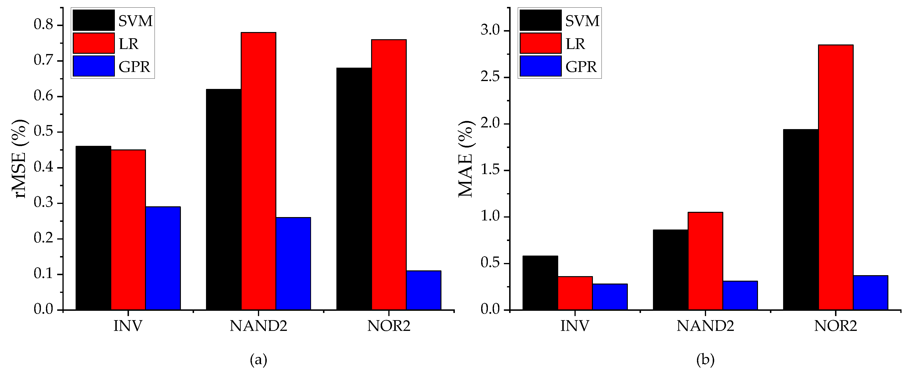
In this section, the accuracy of the GPR model is compared with the linear regression and support vector machine (SVM) obtained from Scikit-Learn framework [23]. For LR, we use the Ordinary least squares Linear Regression model. For SVM, 𝜖-SVR model is selected with the RBF kernel, where C was tuned within [1 × 10⁻⁵, 1 × 10⁵] and gamma was tuned within [1 × 10⁻², 1]. Epsilon in SVR was tuned within [0.001, 0.1]. For GP, the GPR model with a composite kernel, including RBF, RQ and linear kernel, for modeling the covariance matrix to improve the generalization of the model. The RBF kernel’s length scale was allowed to vary between 1 × 10⁻¹⁰ and 1 × 10³ during the training process and the overall model noise variance was set to 1.0 by default. The rRMSE and MAE of different ML methods are shown in Figure 5a,b, respectively, where the proposed GPR model exhibits the best predictive performance.

4.2.3. Verification of the SGED Framework

This section evaluates the proposed SGED framework as shown in Figure 3. As mentioned before, the statistical characteristics of gate delay, i.e., mean and standard deviation value, can be calculated based on a collection of data composed of 10,000-point GPR predicting results.
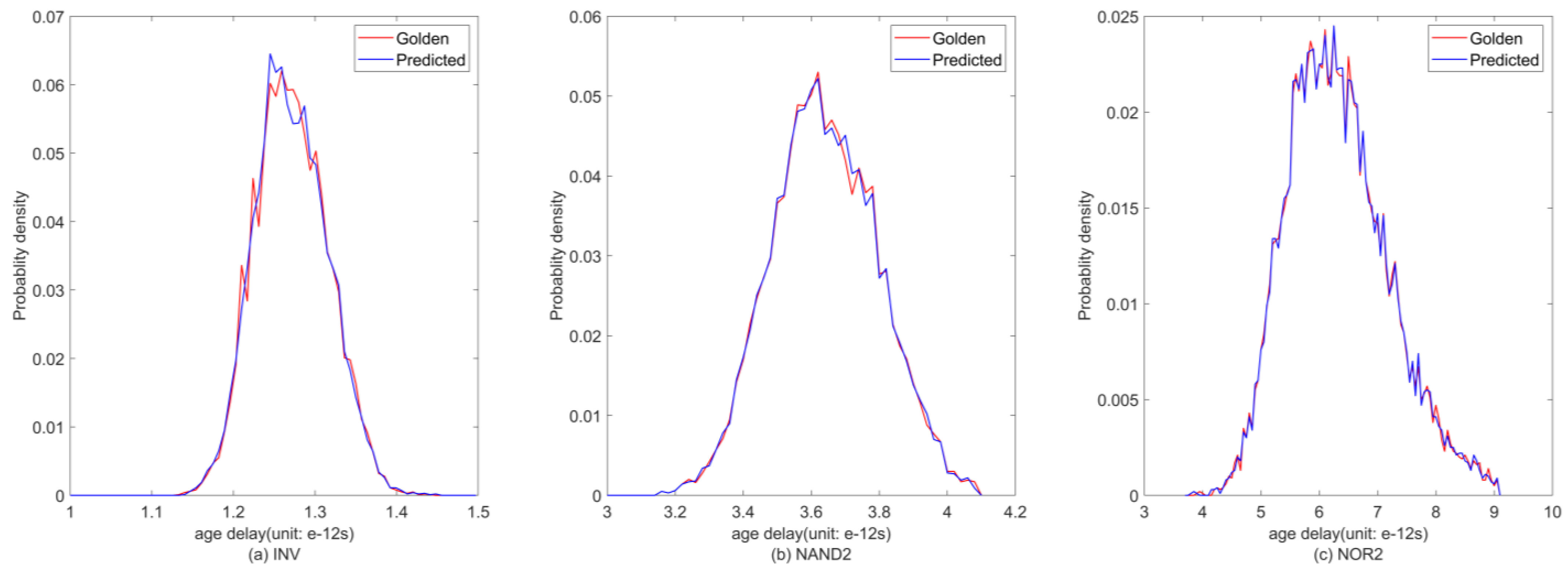
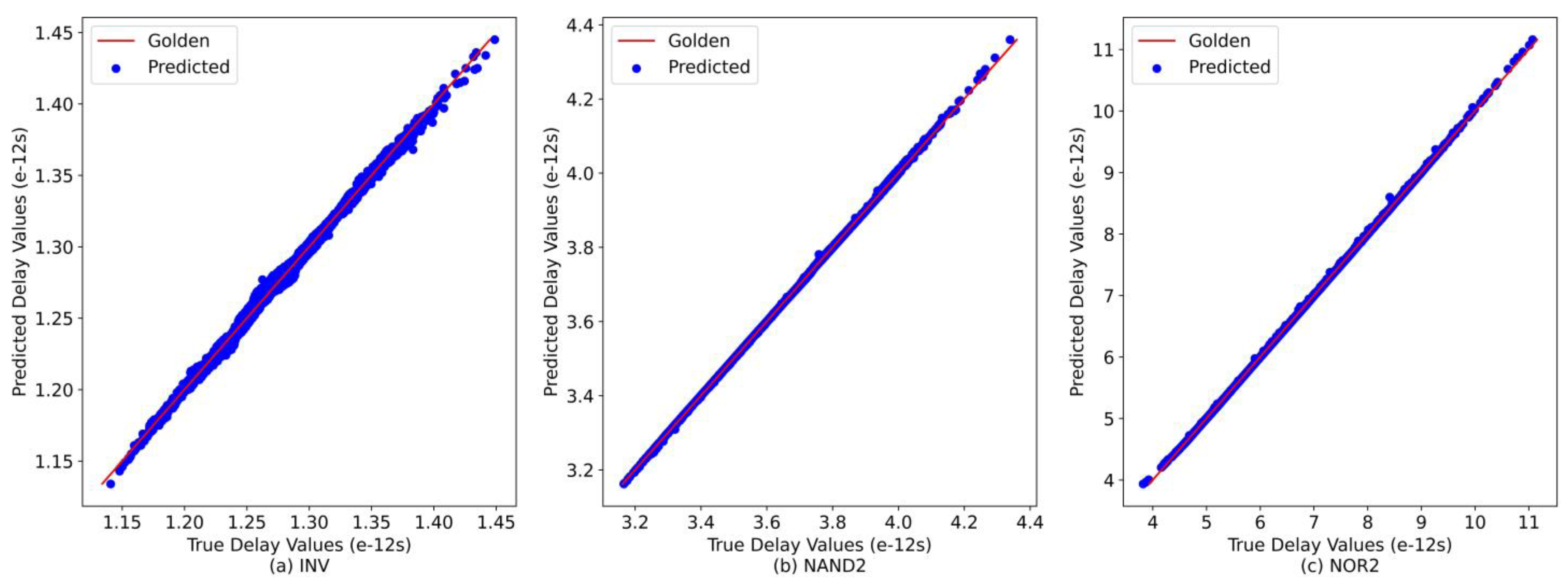
As shown in Table 4, the suggested SGED framework has an excellent performance in the mean ( μ ) and the standard deviation ( σ ) prediction with high accuracy compared to the golden data. The lower the Abs.E is, the better prediction and fitting performance of the SGED framework are. Figure 6 outlines the probability density of the golden and predicted results for INV, NAND2, and NOR2, which show a good agreement between the two datasets. To cast more light on the prediction accuracy, we also include a scatter plot for three gates shown in Figure 7. It shows that our predicted results are close to the values obtained from the Hspice simulation.
The computational process overhead can be significantly reduced by the proposed method, nearly a speedup beyond three orders of magnitude. Every 10,000-point test data take about 4 h for the Hspice simulation, which is performed on Intel Xeon Gold 5118 2.3 GHz CPU. While SGED only takes about 6 s for the same number of test data performed on Intel i7-10700k 2.9 GHz CPU. Exhaustive Hspice simulation is strongly associated with the number of transistors inside the gate and thus is time-consuming work. However, the runtime of ML methods barely changed.

4.2.4. Accuracy Comparation between SGED and Other Literature

In order to verify the accuracy of our proposed SGED framework, comparisons are made between our experimental result and other literature [12], as shown in Table 5. Abs.E ( μ ) represents the absolute error of mean   value , Abs.E ( σ ) and so on. What needs to be pointed out here is that, for the sake of fairness, this experiment will be performed by 45 nm Nangate FreePDK45 instead of commercial 28 nm technology, and the standard deviations of PVs are set as 10% of each mean value. The implementation results show that our proposed SGED framework is better than the literature.

5. Conclusions

Device parameters that determine circuit performance will change over time Moreover, the impact of NBTI is exacerbated by PV, which results in greater variability in circuit performance. This paper proposes a GPR based framework, i.e., SGED, to evaluate the variation of gate delay by jointly considering the NBTI and PV effect. The experimental results show that our suggested framework can greatly reduce the runtime while ensuring accuracy.
In future work, more variable features will be integrated into the GPR model, such as temperature, stress time, stress probability, etc. On the other hand, the SGDE framework can also be applied to the circuit level for analyzing the variation of path delay.

Author Contributions

Conceptualization: A.B.; software: R.W.; data curation: A.B.; writing—original draft preparation: A.B.; writing—review and editing: S.J.; supervision: J.L.; project administration: J.L.; funding acquisition: J.L. All authors have read and agreed to the published version of the manuscript.

Funding

This work was supported in part by the National Key Research and Development Program of China (Grant No. 2019YFB2205004), and in part by the National Natural Science Foundation of China under Grant (62174031) and in part by the Jiangsu Natural Science Foundation (Grant No. BK20201233) and in part by the SEU-SMIT EDA Joint Laboratory Project.

Conflicts of Interest

The authors declare no conflict of interest.

References

  1. Khalil, K.; Eldash, O.; Kumar, A.; Bayoumi, M. Machine Learning-Based Approach for Hardware Faults Prediction. IEEE Trans. Circuits Syst. I Regul. Pap. 2020, 67, 3880–3892. [Google Scholar] [CrossRef]
  2. Moghaddasi, I.; Nasab, M.E.S.; Kargahi, M. Aging-Aware Instruction-Level Statistical Dynamic Timing Analysis for Embedded Processors. IEEE Trans. Very Large Scale Integr. (VLSI) Syst. 2020, 28, 433–442. [Google Scholar] [CrossRef]
  3. Hiroaki, K.; Yukio, M.; Masanori, H.; Takao, O. Comparative study on delay degrading estimation due to NBTI with circuit/instance/transistor-level stress probability consideration. In Proceedings of the 11th International Symposium on Quality Electronic Design, San Jose, CA, USA, 22–24 March 2010; pp. 646–651. [Google Scholar]
  4. Copetti, T.; Medeiros, G.; Poehls, L.B.; Vargas, F.; Kostin, S.; Jenihhin, M.; Raik, J.; Ubar, R. Gate-level modelling of NBTI-induced delays under process variations. In Proceedings of the 2016 17th Latin-American Test Symposium (LATS), Foz do Iguacu, Brazil, 6–8 April 2016; pp. 75–80. [Google Scholar]
  5. Yinghai, L.; Li, S.; Hai, Z.; Hengliang, Z.; Fan, Y.; Xuan, Z. Statistical reliability analysis under process variation and aging effects. In Proceedings of the 2009 46th ACM/IEEE Design Automation Conference, San Francisco, CA, USA, 26–31 July 2009; pp. 514–519. [Google Scholar]
  6. Naphade, T.; Goel, N.; Nair, P.R.; Mahapatra, S. Investigation of stochastic implementation of reaction diffusion (RD) models for NBTI related interface trap generation. In Proceedings of the 2013 IEEE International Reliability Physics Symposium, Anaheim, CA, USA, 14–18 April 2013; pp. XT.5.1–XT.5.11. [Google Scholar]
  7. Vattikonda, R.; Wang, W.; Cao, Y. Modeling and minimization of PMOS NBTI effect for robust naometer design. In Proceedings of the 2006 Design Automation Conference, San Francisco, CA, USA, 24–28 July 2006; pp. 1047–1052. [Google Scholar]
  8. Bhardwaj, S.; Wang, W.; Vattikonda, R.; Cao, Y.; Vrudhula, S. Predictive Modeling of the NBTI Effect for Reliable Design. In Proceedings of the IEEE Custom Integrated Circuits Conference 2006, San Jose, CA, USA, 10–13 September 2006; pp. 189–192. [Google Scholar]
  9. Siddiqua, T.; Gurumurthi, S.; Stan, M.R. Modeling and analyzing NBTI in the presence of Process Variation. In Proceedings of the 2011 12th International Symposium on Quality Electronic Design, Santa Clara, CA, USA, 14–16 March 2011; pp. 1–8. [Google Scholar]
  10. Li, B.; Hashimoto, M.; Schlichtmann, U. From Process Variations to Reliability: A Survey of Timing of Digital Circuits in the Nanometer Era. IPSJ Trans. Syst. LSI Des. Methodol. 2018, 11, 2–15. [Google Scholar] [CrossRef] [Green Version]
  11. Khalid, U.; Mastrandrea, A.; Olivieri, M. Effect of NBTI/PBTI aging and process variations on write failures in MOSFET and FinFET flip-flops. Microelectron. Reliab. 2015, 55, 2614–2626. [Google Scholar] [CrossRef] [Green Version]
  12. Han, S.; Kim, J. NBTI-aware statistical timing analysis framework. In Proceedings of the 23rd IEEE International SOC Conference, Las Vegas, NV, USA, 27–29 September 2010; pp. 158–163. [Google Scholar]
  13. Kleeberger, V.B.; Graeb, H.; Schlichtmann, U. Predicting future product performance: Modeling and evaluation of standard cells in FinFET technologies. In Proceedings of the 50th ACM/EDAC/IEEE Design Automation Conference (DAC), San Francisco, CA, USA, 29 May–7 June 2013; pp. 1–6. [Google Scholar]
  14. Alpaydin, E. Introduction to Machine Learning, 4th ed.; MIT Press: Cambridge, MA, USA, 2020. [Google Scholar]
  15. Geyik, C.S.; Zhang, Z.; Aygün, K.; Aberle, J.T. Machine Learning for Evaluating the Impact of Manufacturing Process Variations in High-Speed Interconnects. In Proceedings of the 2021 22nd International Symposium on Quality Electronic Design (ISQED), Santa Clara, CA, USA, 7–9 April 2021; pp. 160–163. [Google Scholar]
  16. Tripathi, J.N.; Vaghasiya, H.; Junjariya, D.; Chordia, A. Machine Learning Techniques for Modeling and Performance Analysis of Interconnects. IEEE Open J. Nanotechnol. 2021, 2, 178–190. [Google Scholar] [CrossRef]
  17. Nguyen, T.A.; Shi, B.; Ma, H.; Li, E.P.; Chen, X.; Cangellaris, A.C.; Schutt-Ainé, J. Comparative Study of Surrogate Modeling Methods for Signal Integrity and Microwave Circuit Applications. IEEE Trans. Compon. Packag. Manuf. Technol. 2021, 11, 1369–1379. [Google Scholar] [CrossRef]
  18. Koriyama, T.; Oshio, S.; Kobayashi, T. A speaker adaptation technique for Gaussian process regression based speech synthesis using feature space transform. In Proceedings of the 2016 IEEE International Conference on Acoustics, Speech and Signal Processing (ICASSP), Shanghai, China, 20–25 March 2016; pp. 5610–5614. [Google Scholar]
  19. Li, Z.; Deng, C.; Zhao, B.; Tian, Y.; Huang, Y. Hyperspectral inversion for soil moisture and temperature based on Gaussian process regression. In Proceedings of the 2019 IEEE International Conference on Signal, Information and Data Processing (ICSIDP), Chongqing, China, 11–13 December 2019; pp. 1–4. [Google Scholar]
  20. Fezai, R.; Mansouri, M.; Bouguila, N.; Nounou, H.; Nounou, M. Reduced Gaussian process regression for fault detection of chemical processes. In Proceedings of the 2019 International Conference on Internet of Things, Embedded Systems and Communications, IINTEC 2019, Gammarth, Tunisia, 20–22 December 2019; pp. 186–191. [Google Scholar]
  21. Trinchero, R.; Canavero, F. Machine Learning Regression Techniques for the Modeling of Complex Systems: An Overview. IEEE Electromagn. Compat. Mag. 2021, 10, 71–79. [Google Scholar] [CrossRef]
  22. Gpflow. Available online: https://www.gpflow.org/ (accessed on 11 April 2022).
  23. Pedregosa, F.; Varoquaux, G.; Gramfort, A.; Michel, V.; Thirion, B.; Grisel, O.; Blondel, M.; Prettenhofer, P.; Weiss, R.; Dubourg, V.; et al. Scikit-learn: Machine Learning in Python. J. Mach. Learn. Res. 2011, 12, 2825–2830. [Google Scholar]
Figure 1. The probability density of V t h considering PV and NBTI&PV.
Electronics 11 01336 g001
Figure 2. The overall GPR training and predicting process.
Electronics 11 01336 g002
Figure 3. The SGDE framework using GPR learning interface.
Electronics 11 01336 g003
Figure 4. Accuracy comparation between different GPR kernel: (a) rMSE comparation; (b) MAE comparation.
Electronics 11 01336 g004
Figure 5. Accuracy comparation between different ML methods: (a) rMSE comparation (b) MAE comparation.
Electronics 11 01336 g005
Figure 6. The probability density of the golden and predicted test data: (a) INV gate; (b) NAND2 gate; (c) NOR2 gate.
Electronics 11 01336 g006
Figure 7. Model prediction accuracy comparison for: (a) INV gate; (b) NAND2 gate; (c) NOR2 gate.
Electronics 11 01336 g007
Table 1. Process parameters with nominal values and variation assumptions.
PV Source u σ
V t h 0 −0.39 V 0.05   u
T o x 1.485 nm0.05 u
XL3.5 nm0.05 u
XW18 nm0.05 u
Table 2. The statistical characteristics of Δ V t h by separate PV source.
PV Sourceμ (mV)σ (mV)
Vth059.10.53559
Tox59.12.3012
XL59.12.9589 × 10−3
XW59.11.0208 × 10−3
Table 4. The statistical accuracy of SGDE framework.
μ   ( × 10 12   s ) σ   ( × 10 12   s )
GoldenProposedAbs.EGoldenProposedAbs.E
INV1.27491.27550.087%0.044130.043820.621%
NAND3.65173.65400.026%0.158790.160120.011%
NOR6.38366.37810.033%0.915220.905180.583%
Table 5. Accuracy comparation with literature [12].
Abs . E   ( μ ) Abs . E   ( σ )
ProposedLiterature [12]ProposedLiterature [12]
INV0.052%0.20%0.701%1.21%
NAND0.062%0.12%0.838%1.94%
NOR0.086%0.13%1.097%2.08%
Publisher’s Note: MDPI stays neutral with regard to jurisdictional claims in published maps and institutional affiliations.