Article

A 1200 V SiC Trench MOSFET with a Laterally Widened P-Shield Region to Enhance the Short-Circuit Ruggedness

1
Institute of Microelectronics of the Chinese Academy of Sciences, Beijing 100029, China
2
University of Chinese Academy of Sciences, Beijing 100049, China
*
Authors to whom correspondence should be addressed.
Electronics 2022, 11(7), 1077; https://doi.org/10.3390/electronics11071077
Submission received: 28 February 2022 / Revised: 25 March 2022 / Accepted: 28 March 2022 / Published: 29 March 2022
(This article belongs to the Section Power Electronics)

Abstract

:
In this paper, a novel 1200 V SiC trench MOSFET with a laterally widened P-shield region (LW-MOSFET) is presented by using the two-dimensional numerical simulation. Compared with the conventional trench MOSFET (CT-MOSFET), the LW-MOSFET demonstrates an effective enhancement on the short-circuit (SC) reliability and the optimization of static performance simultaneously. According to the simulation results, the SC withstand time (SCWT) of the LW-MOSFET at 600 V DC bus voltage can reach 8 μs, while that of the CT-MOSFET is only 3 μs at the same conditions. The main reason is that the laterally widened P-shield region can help to suppress the saturation current and mitigate the huge current accumulation near the trench area, leading to an enhancement of the SC reliability. Moreover, the Baliga’s FOM of the proposed structure is improved by 45.7%, which benefits from the higher breakdown voltage (BV) and the lower specific on-state resistance (Ron, sp) by using the optimized structure. The advantage of static performance is related to the local charge balance behavior provided by the laterally widened P-shield region, which helps to use a higher doped current spread layer (CSL) without bringing a degeneration of BV.

1. Introduction

Silicon-Carbide (SiC) has become the most promising semiconductor material in the field of power electronics due to its advantages of wide energy band gap, low intrinsic carrier concentration and high breakdown electric field [1,2]. Therefore, the SiC MOSFETs may replace the Si IGBT in the area of high frequency, high voltage and high-power applications [3]. In recent years, many studies on SiC MOSFETs have been conducted to improve device performance. The proposal of trench gate eliminates the JFET region compared with the planar SiC MOSFET, thereby reducing the on-resistance and increasing the power density [4,5]. The short-circuit (SC) failure is one of the common reliability issues in the application of power devices; thus, how to improve the device’s robustness to reduce the failure risk during the SC process is a long-term challenge. According to previous research [6,7,8,9,10,11,12], the SiC MOSFETs present a weaker SC robustness compared with Si devices. For the SiC trench MOSFET, a shorter SC withstand time (SCWT) was found in the recent comparative investigations due to its high current density [13,14,15,16]. Although various studies on the SC characteristics of SiC MOSFETs have been reported [17,18,19], the investigation on the SC reliability enhancement still needs to be studied further, especially for the trench MOSFET structure.
In this article, we proposed a novel SiC trench MOSFET with the laterally widened P-shield region (LW-MOSFET) to improve the SC ruggedness. The static parameters and SC performance have been studied by using the Sentaurus TCAD mix-mode simulation tool [20]. Results indicate that the SCWT of the optimal LW-MOSFET can be improved significantly. Meanwhile, a better static performance is also achieved.

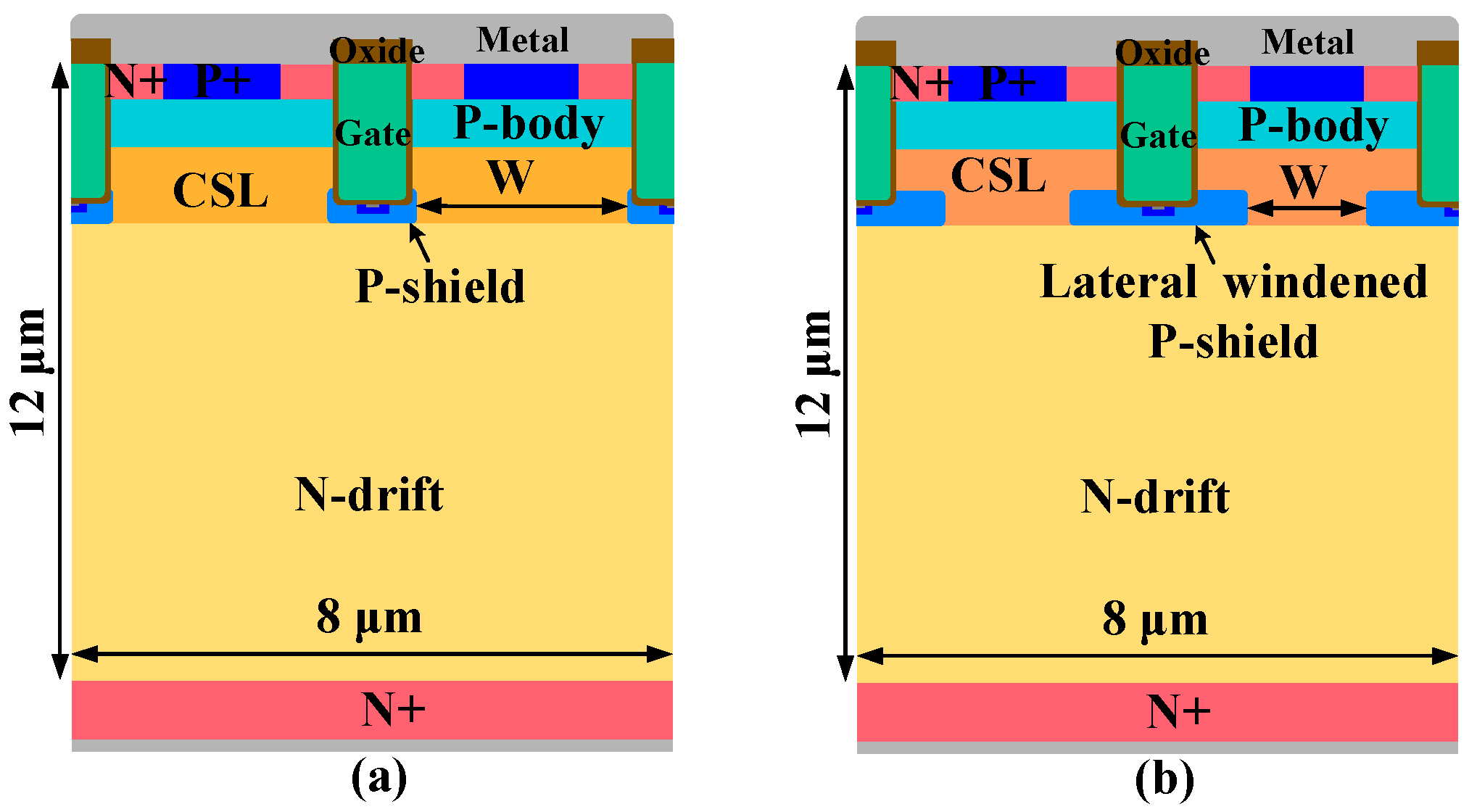
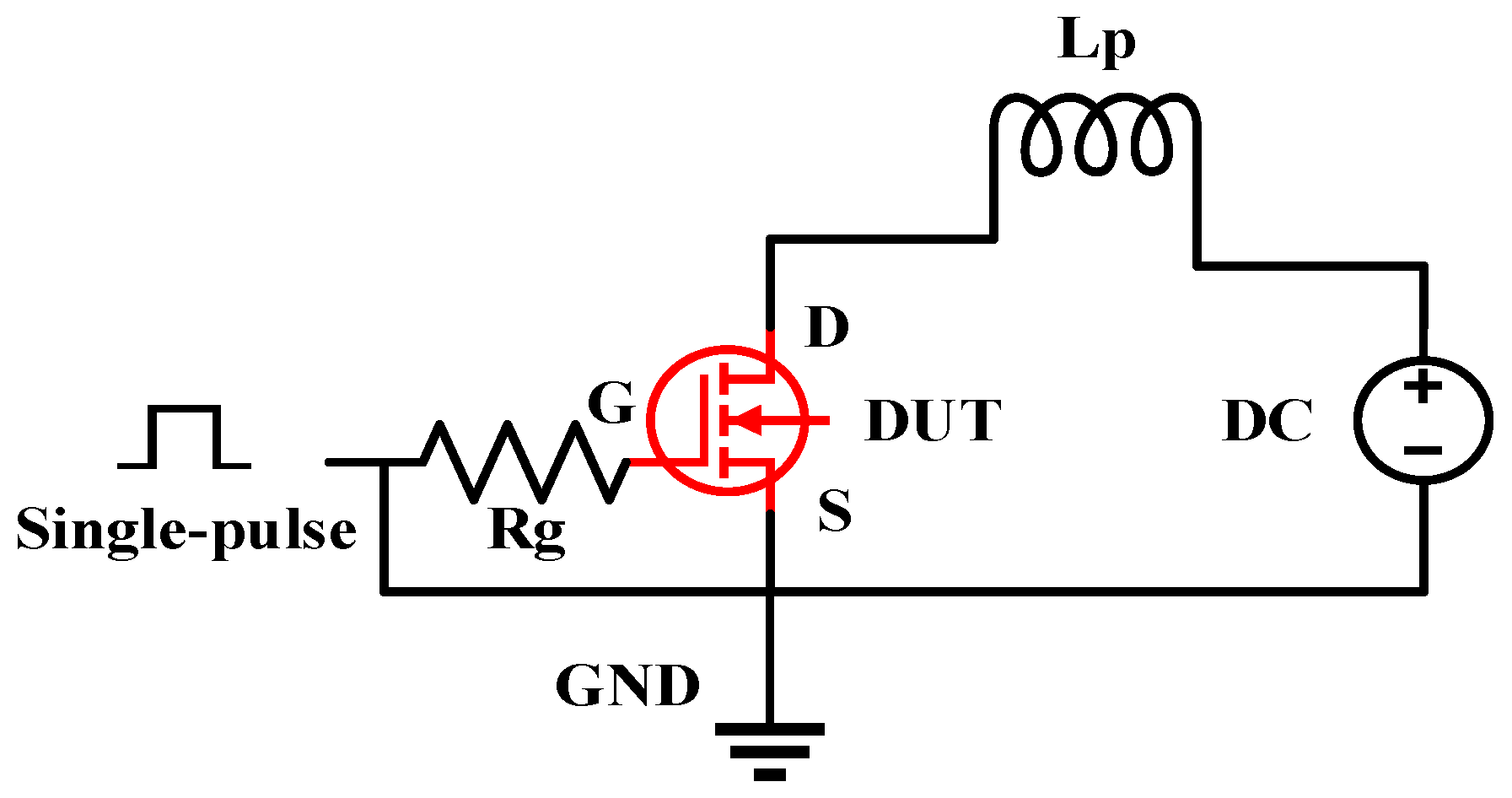
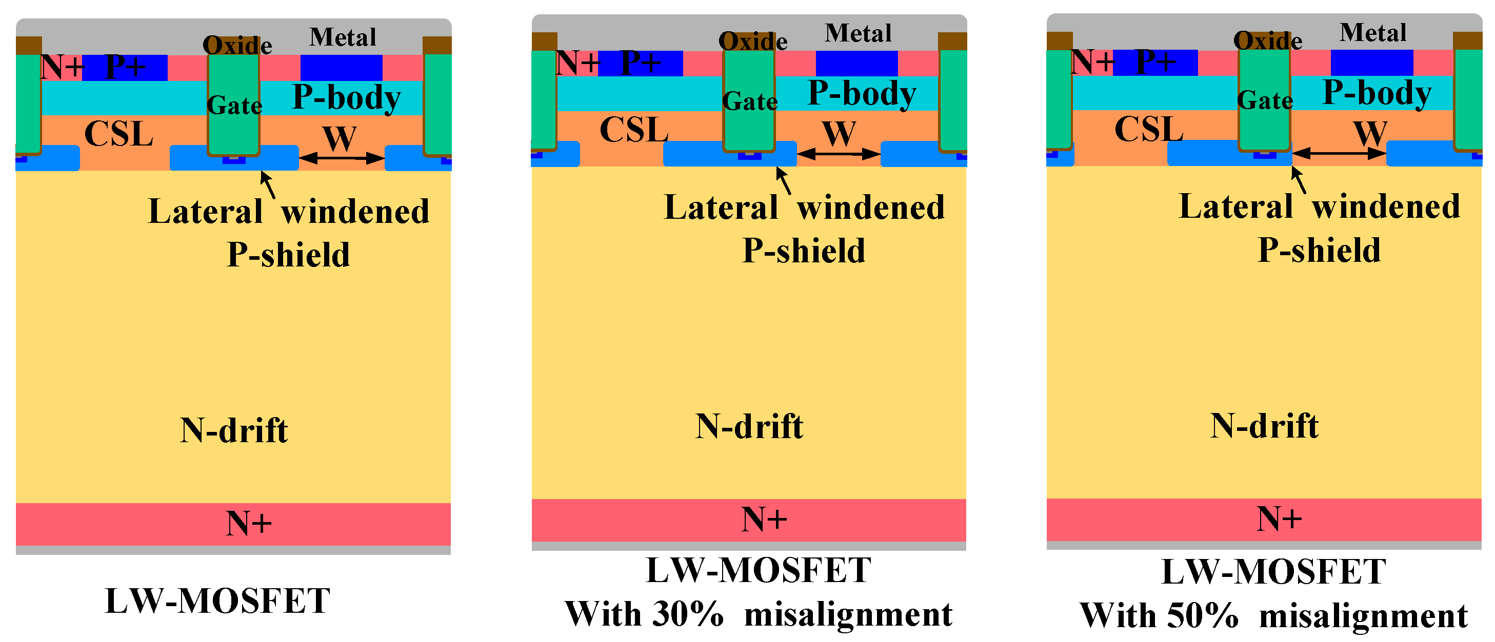
2. Device Structures and Simulation Models

Figure 1 shows the schematic cross-sectional diagram of the conventional trench MOSFET (CT-MOSFET) and the proposed LW-MOSFET. For the two devices, the cell pitch is 4 μm, the thickness of the epitaxy is 12 μm and the doping concentration of the drift layer is 3 × 1015 cm−3. The channel length and P-body doping concentration are set to 0.8 μm and 1.5 × 1017 cm−3 for achieving the same threshold voltage (Vth). The gate oxide thickness is selected to 50 nm. The channel electron mobility of 20 cm2/(V·s) is used in this simulation. Additionally, the lifetimes of the electrons and holes are 2.5 μs and 0.5 μs in the simulation, respectively. The active area of the chip in this article is designed with 14 mm2. For the conventional SiC trench MOSFET, the P-shield region is designed to protect the bottom of gate oxide at the high electric field condition, and the current spread layer (CSL) is added to optimize the on-current capability.
The proposed LW-MOSFET features the laterally widened P-shield region and higher doped CSL compared with the CT-MOSFET, as shown in Figure 1b. The W represents the distance between two widened P-shield regions. Moreover, the manufacturing process of the proposed structure is fully compatible with the standard CT-MOSFET, and only requires additional buried p-layer process adjustment. The detailed structure parameters are summarized in Table 1.
In this simulation, the suitable physics models are used to analyze the device performance. The mobility models including the incomplete ionization, the mobility degradation with the normal electric field (Enormal) and Inversion and Accumulation Layer Mobility model (IALMob), the carrier recombination models considering the Shockley-Read-Hall (SRH), the Auger recombination and the anisotropic avalanche (Okuto-Crowell) are employed. Moreover, the thermodynamic model is also utilized to describe the electrothermal behavior during the SC process. It can accurately describe the lattice temperature distribution and correctly predict the electrical device’s behavior. Additionally, a drain contact thermal resistance of 3 × 10⁻² cm2·K/W [7,21] is considered to describe the heat behavior. Moreover, it is an ideal criterion without considering the package-related influence for the simplifying simulation purpose.

3. Results and Discussion

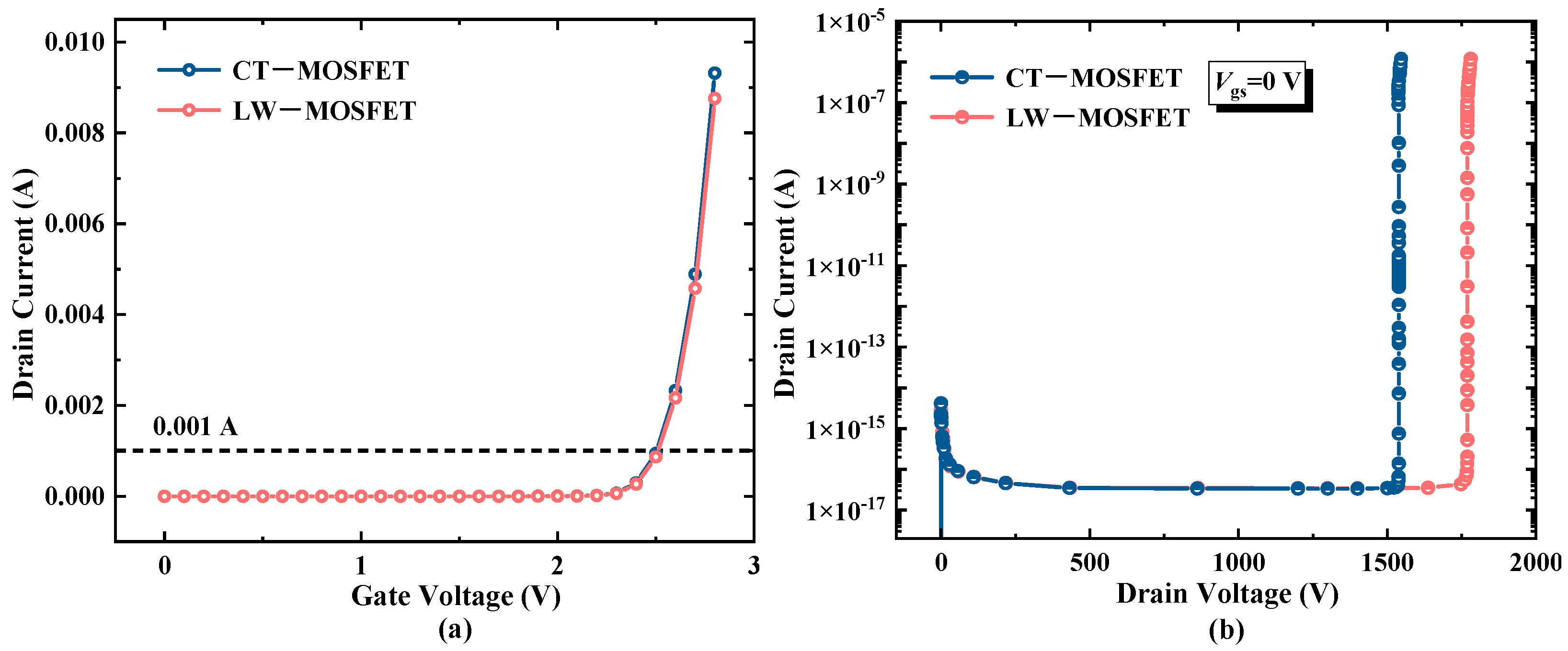
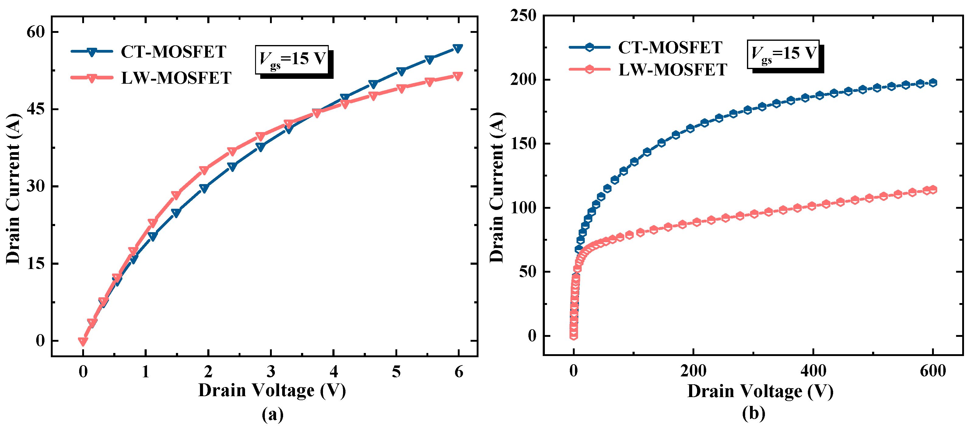
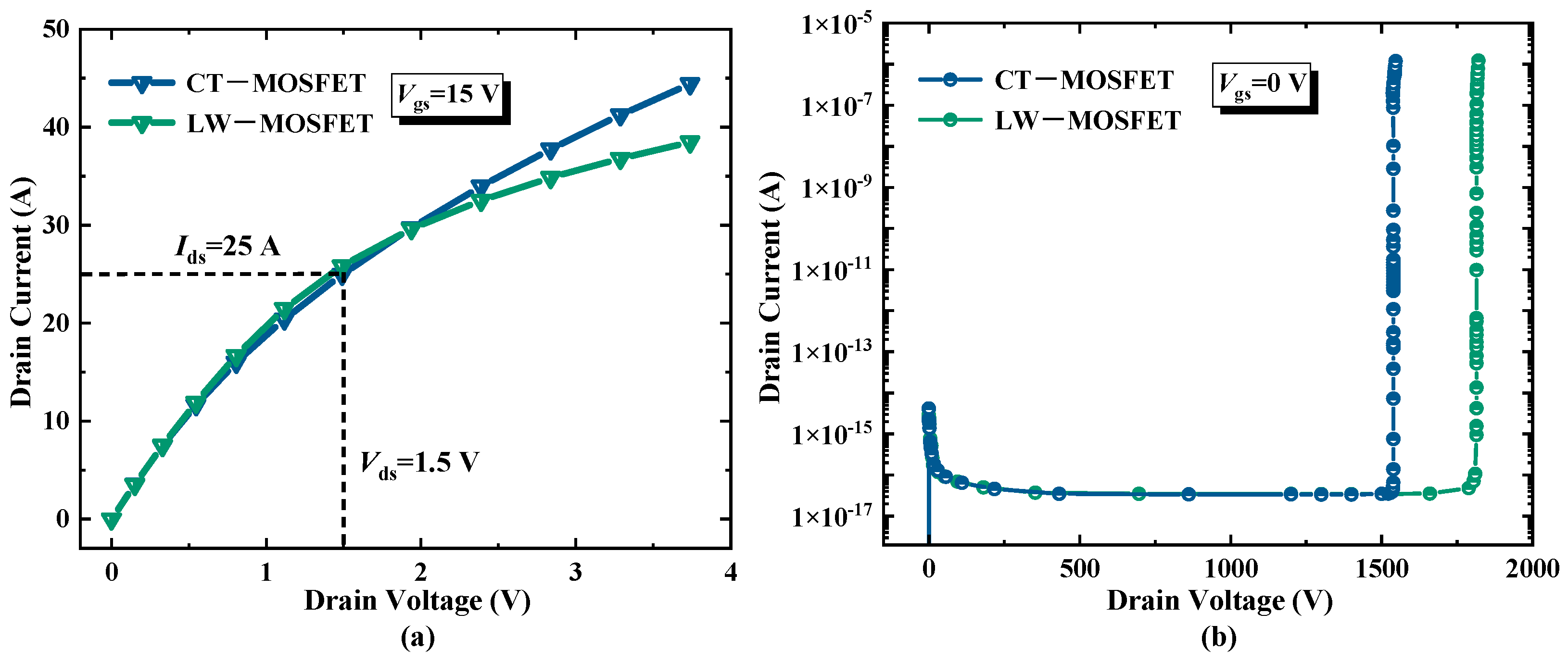
3.1. Static Parameters

Figure 2a,b show the threshold voltage (Vth) and the blocking characteristic curves of the CT-MOSFET and LW-MOSFET, respectively. According to Figure 2, the Vth of the two MOSFETs is 2.5 V at Ids = 1 mA, and the breakdown voltages (BVs) of the CT-MOSFET and LW-MOSFET at Ids = 1 μA are 1547 V and 1780 V. It can be known that a better forward voltage blocking ability is acquired in the LW-MOSFET. The excellent BV of the LW-MOSFET is attributed to the local charge balance between the widened P-shield and the adjusted N-type CSL region.
The electric field distributions of the two devices at Vds = 1200 V and breakdown voltage are shown in Figure 3. It can be seen that the high electric field concentration at the bottom of P-shield region is alleviated in the proposed LW-MOSFET. At Vds = 1200 V, the maximal E-field at the gate oxide (Eox) area is about 0.8 MV/cm for the LW-MOSFET, which is smaller than the CT-MOSFET with about 1.5 MV/cm. Additionally, the critical gate oxide E-fields at the breakdown voltage of the CT-MOSFET and LW-MOSFET are ~2.4 MV/cm and ~1.3 MV/cm, respectively. Therefore, the gate oxide of the LW-MOSFET has better protection at the high electric field due to the great shielding effect of the laterally widened P-shield region.
Figure 4 shows the simulation results of the forward I-V characteristic curves for the two devices. It can be found that the specific on-state resistances (Ron, sp) of the CT-MOSFET and LW-MOSFET are 6.86 mΩ·cm2 and 6.26 mΩ·cm2, respectively. The lower Ron, sp of the LW-MOSFET is because the lateral widening of the P-shield allows the increase in CSL doping concentration without sacrificing the BV ability. However, a higher doping concentration of CSL in the CT-MOSFET is limited due to the degeneration of BV characteristics. Therefore, the LW-MOSFET can provide a better compromise between the on-state current and the blocking ability.
The Baliga’s figure of merit (Baliga’s FOM = BV2/Ron, sp) of the CT-MOSFET and LW-MOSFET are 0.35 kV2·mΩ−1·cm−2 and 0.51 kV2·mΩ−1·cm−2, respectively. It means that the proposed LW-MOSFET has an improvement of 45.7% on static performance than CT-MOSFET. In addition, as shown in Figure 4b, the saturation currents of the two devices at Vds = 600 V are 197.5 A and 114.1 A, respectively. Therefore, the proposed CT-MOSFET demonstrates a lower saturation current, leading to the superior SCWT ability as proved by the following SC simulation results.

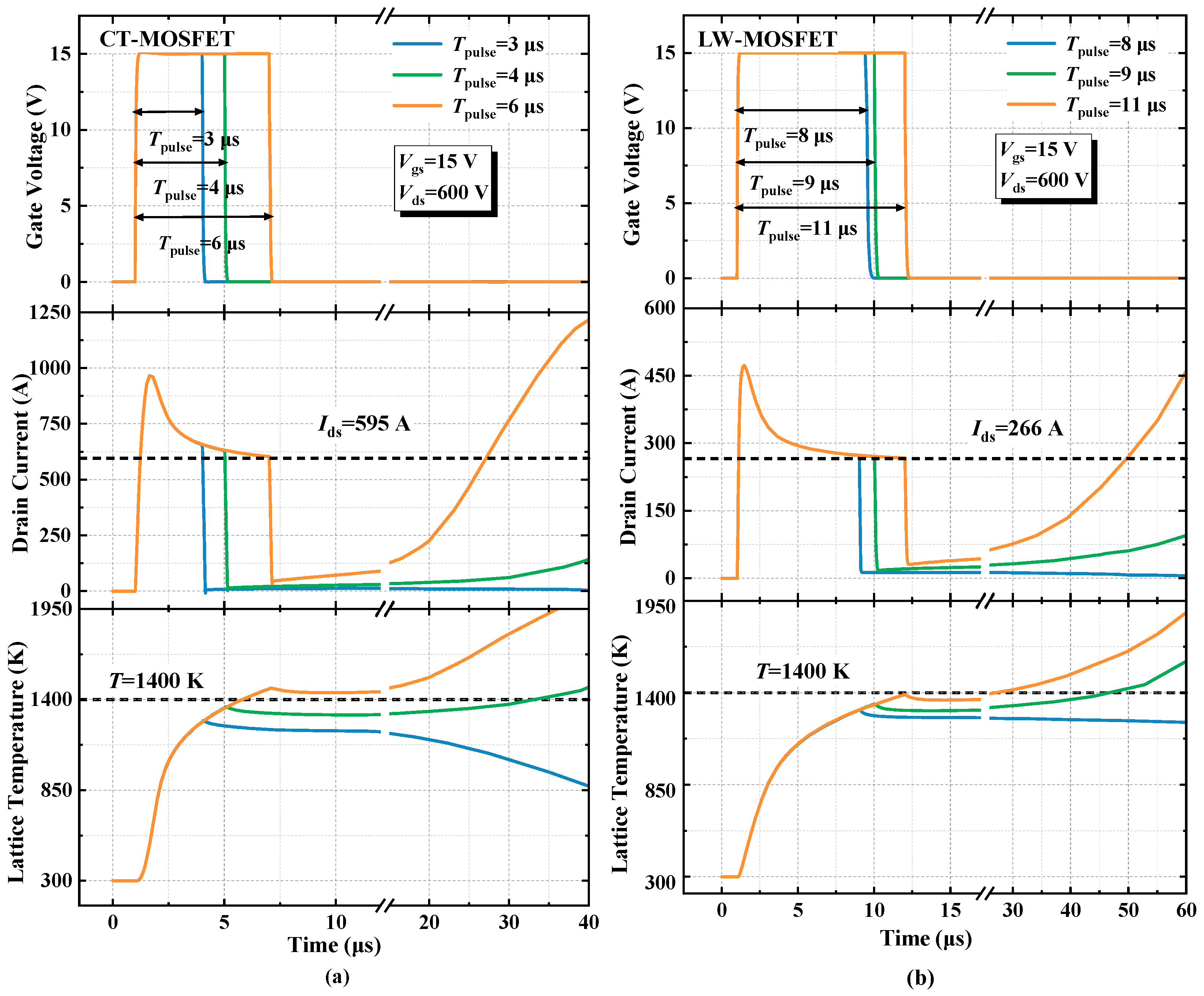
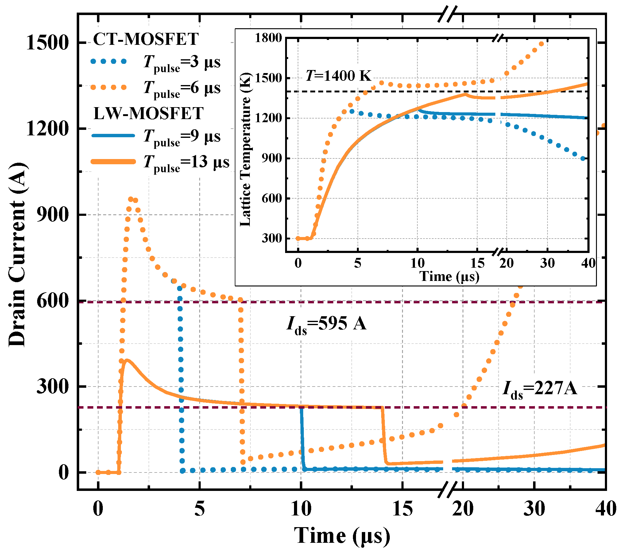
3.2. SC Simulation Results and Analysis

The circuit shown in Figure 5 is used to simulate the SC process. In the circuit topology, the parasitic inductance (Lp) is set to 200 nH, the gate resistance (Rg) is 2.5 Ω and DC drain-source voltage is 600 V. In addition, the single gate pulse Vgs is switched between 0 V to 15 V with varied pulse time, which controls the SC times applied to the device under test (DUT).
According to the SC waveforms shown in Figure 6, the SC current Ids increases sharply and then decreases gradually to the saturated state. This waveforms behavior can be explained by the channel carrier mobility variation. At the beginning of the SC process, the increase in inversion charge and the decrease in the interface charge contribute to the weakening of Coulomb scattering mechanism, which in turn leads to the rise of Ids. Then, the enhancement of surface roughness scattering and phonon scattering induced by the high lattice temperature causes the subsequent decline in carrier mobility and Ids.
From the SC simulation curves under different SC pulses shown in Figure 6a, the SC saturation current of CT-MOSFET is 595 A. It can be seen that the CT-MOSFET returns to the normal state when the SC pulse time (Tpulse) is 3 μs. However, if the Tpulse is over 4 μs, the rising drain tail current and lattice temperature with positive feedback are found although the gate signal is already turned off. In general, it is hard for SiC MOSFETs to survive short heating above 1300–1500 K owing to oxide or contact metal failure [22]. Therefore, the failure boundary condition is defined at the lattice temperature over 1400 K. It can be seen in Figure 6a that the lattice temperature of CT-MOSFE exceeds 1400 K due to the thermal runaway when the Tpulse is over 4 μs, and eventually leads to the device’s burnout. Therefore, the simulation results indicate that the safety SCWT of the CT-MOSFET is 3 μs at Vds = 600 V and Vgs = 15 V.
The proposed LW-MOSFET is simulated at the same bias conditions, as shown in Figure 6b. It can be seen that the SC saturation current of LW-MOSFET is 266 A, which is greatly lower than that of CT-MOSFET. More importantly, the SCWT is increased to 8 μs without device failure, which means an improvement of about three times on SC reliability. Table 2 shows the parameters comparison of CT-MOSFET and LW-MOSFET summarized from the above simulation results.
As can be observed in Figure 6, although the SC pulse is within the SCWT (Tpulse = 3 μs for CT-MOSFET and Tpulse = 8 μs for LW-MOSFET), the Ids of the device is not completely reduced to 0 A after the gate is turned off. The tail current is formed by carriers generated under the combined action of high voltage and increased lattice temperature. However, the tail current of the device does not gradually rise out of control, which due to the power generated inside the device can be transferred out in time. Subsequently, the tail current gradually decreases to the normal turn-off state, correspondingly indicating that the SC pulse is still within the SCWT.

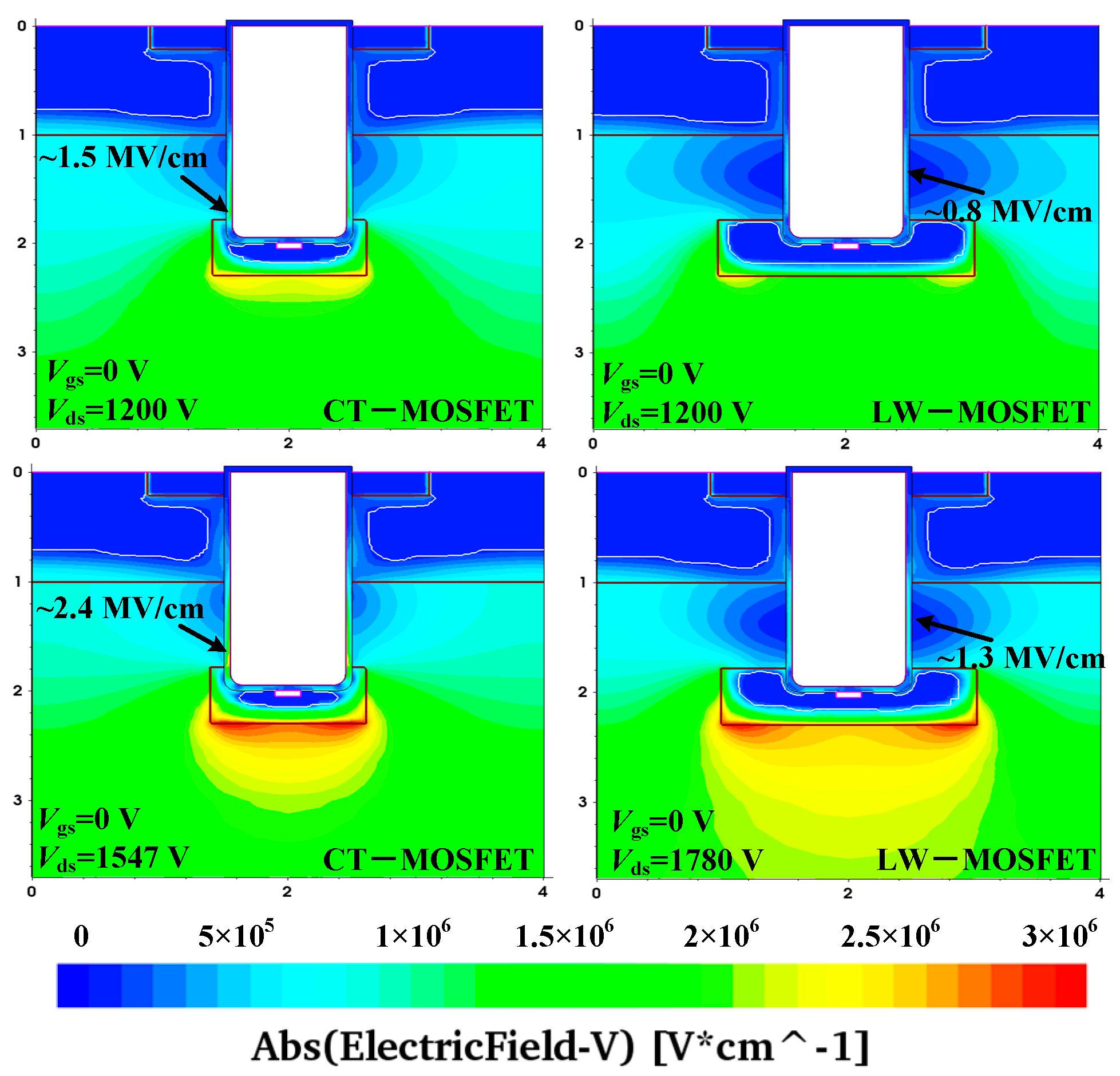
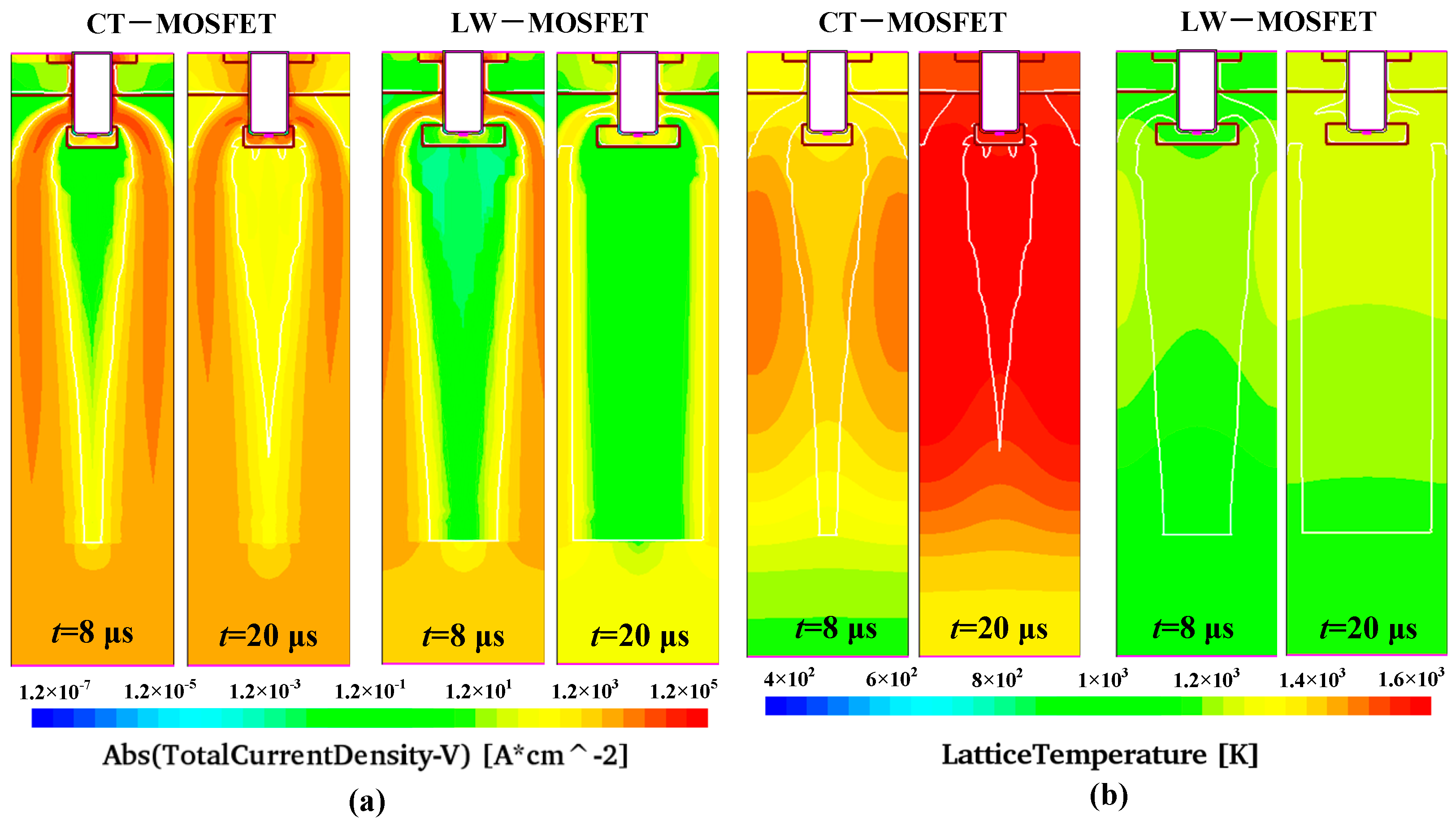
3.3. Analysis of the Internal Physical Mechanism

To verify the physical mechanism of the enhanced SC performance in LW-MOSFET, the same SC pulse time of 8 μs is applied to the two devices for comparative analysis, and the results are shown in Figure 7. It can be seen that the Ids and lattice temperature of LW-MOSFET gradually decrease and return to the normal situation after the 8 μs SC process. However, there is a distinct increase in the Ids and lattice temperature in the CT-MOSFET after the gate signal is turned off. It will eventually cause the burnout of the device due to the thermal runaway.
The current density distribution and lattice temperature distribution of the two devices at t = 8 μs and t = 20 μs are illustrated in Figure 8. From Figure 8a, it can be noted that two adjacent current paths in the proposed structure are separated away by the widened P-shield region compared with that of the CT-MOSFET. Therefore, the current accumulation behavior near the trench region is weakened. Most importantly, the saturation current of the proposed structure is also suppressed due to the further depletion effect produced by the enlarged P-shield region. That is to say, the channel pinch-off behavior is enhanced, leading to a significantly lower saturation current. Based on the above situation, the lattice temperature affected by apparently smaller current density also decreases as shown in Figure 8b. Therefore, the electrothermal coupling effect in the LW-MOSFET is suppressed compared with the CT-MOSFET. Thus, the LW-MOSFET presents a stronger robustness at the harsher SC conditions than the conventional structure.

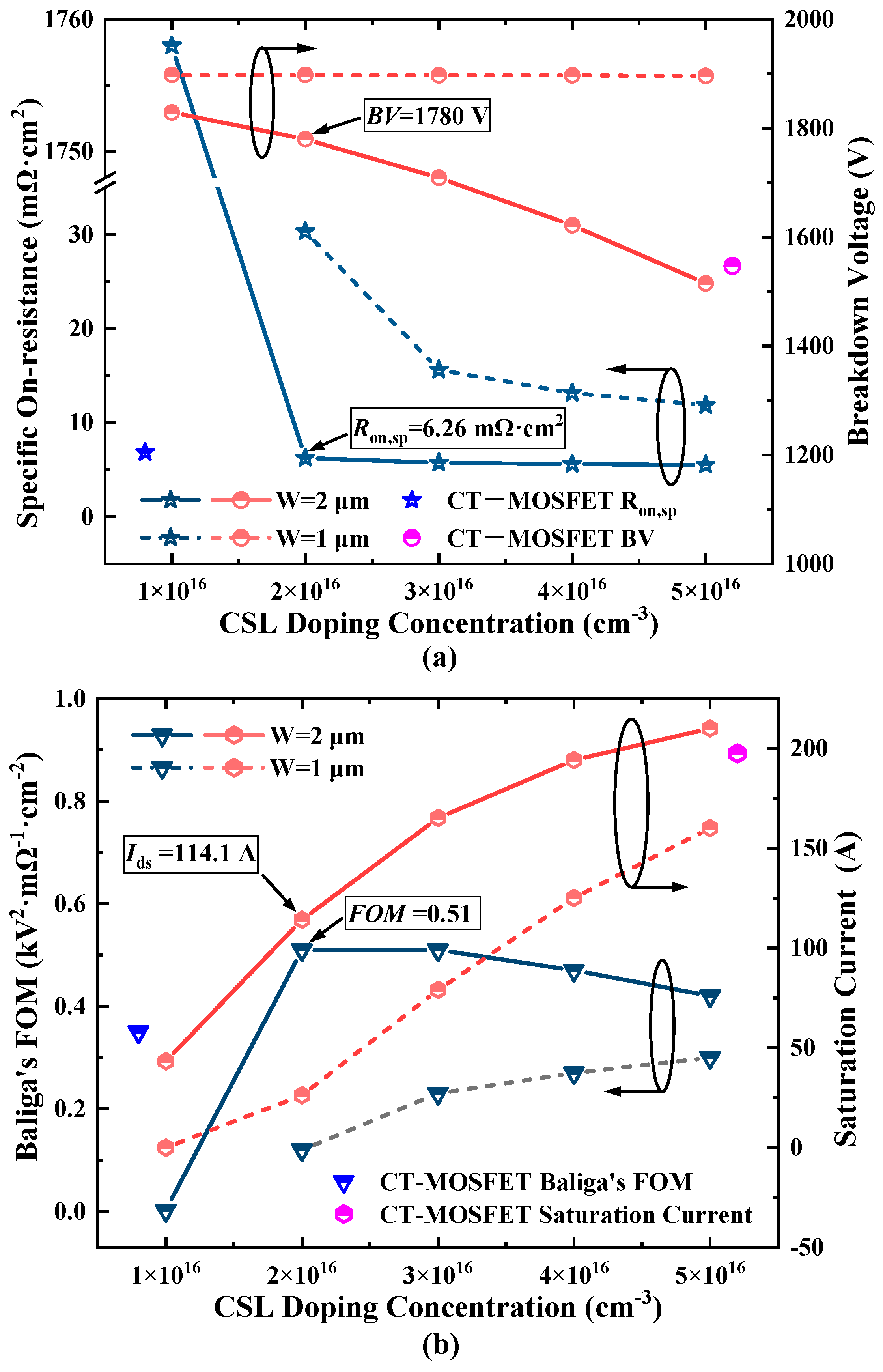
3.4. Structure Parameters Optimization in LW-MOSFET

Within the structural optimization of LW-MOSFET, the influence of the width of the P-shield region and doping concentration of CSL (Ncsl) on the static parameters and SC saturation current are studied further. The simulation results of device performance for the LW-MOSFET with different structural parameters are shown in Figure 9. During the adjustment of structural parameters, the comparison value of W is selected with 1 μm and 2 μm according to the cell pitch of the device, and the Ncsl varies within the range from 1 × 1016 cm−3 to 5 × 1016 cm−3.
It can be obtained from Figure 9 that the BV and Ron, sp of the LW-MOSFET change with the increase in Ncsl. If the W is 1 μm, namely a relatively wider P-shield width, the device’s on-state current ability is severely influenced by the widening of the P-shield region. Therefore, the Ron, sp and Baliga’s FOM performance are inferior to the CT-MOSFET. For the situation of W = 2 μm, the doping Ncsl = 1 × 1016 cm−3 is out of consideration due to the significantly higher Ron, sp value. Additionally, other doping selections may demonstrate a possible acceptable criterion, according to Figure 9a. Therefore, the Baliga’s FOM and the saturation current are compared further to find the best doping situations, as given in Figure 9b. It can be found that the LW-MOSFET with doping of Ncsl = 2 × 1016 cm−3 has both the maximum Baliga’s FOM and the minimum saturation current. Table 3 summarizes the values of BV, Ron, sp, Baliga’s FOM and saturation current at Vds = 600 V for the LW-MOSFET with different structural parameters. After comprehensively analyzing the influence of structural parameters on static parameters and SC performance, the W and Ncsl in optimal LW-MOSFET are identified as 2 μm and 2 × 1016 cm−3, respectively.
In addition, the misalignment situation of the LW-MOSFET between the trench gate and P-shield region is also inspected, as shown in Figure 10, and the simulation results are summarized in Table 4. It can be seen from the simulation data that the static parameters and saturation current of the LW-MOSFET almost keep constant if the misalignment position between trench gate and P-shield region is within 30%, which can meet the most fabrication tolerance. If the misalignment exceeds 40%, the saturation current of the LW-MOSFET is still significantly suppressed, but the static parameters are slightly degraded compared with CT-MOSFET. That means, if the reasonable misalignment situation occurs, the changed LW-MOSFET structure still exhibits a significant optimization on the Baliga’s FOM and saturation current compared with the CT-MOSFET.
Considering the actual application situation, the LW-MOSFET with the same I-V characteristics of the CT-MOSFET is obtained by more detailed adjusting CSL doping concentration and P-shield region width. According to Figure 11a, it can be seen that the LW-MOSFET shows almost the same I-V characteristics as the CT-MOSFET, both devices indicating the same operating current of Ids = 25 A at the Vgs = 15 V and Vds = 1.5 V. In addition, as shown in Figure 11b, the LW-MOSFET also shows a higher breakdown voltage than the CT-MOSFET, and the BVs of the LW-MOSFET and CT-MOSFET are 1820 V and 1547 V, respectively. In this condition, the Baliga’s FOM of the LW-MOSFET is 0.48 kV2·mΩ−1·cm−2. For the above parameter results, the structural dimension of the LW-MOSFET is designed with W = 1.9 μm and Ncsl = 2 × 1016 cm−3.
Moreover, the SC simulation results of two structures performed under Vds = 600 V and Vgs = 15 V are shown in Figure 12. It can be seen that the SC saturation current is 227 A and the SCWT is 9 μs, while that of the CT-MOSFET is 595 A and the SCWT is 3 μs. It indicates that this LW-MOSFET also has significantly stronger SC reliability than the CT-MOSFET. From the above simulation results, it can be concluded that the adjusted LW-MOSFET with similar I-V characteristics as the CT-MOSFET still presents an optimization in the static performance and SC reliability simultaneously.

4. Conclusions

This article presents and investigates a novel short-circuit (SC)-enhanced SiC trench MOSFET with a laterally widened P-shield region (LW-MOSFET) by using Sentaurus TCAD simulation. Two-dimensional simulation results indicate that the proposed LW-MOSFET can achieve superior SC robustness and a good static performance simultaneously. The SCWT of the LW-MOSFET is increased to 8 μs compared with the 3 μs of the CT-MOSFET. The main reason is that the channel pitch-off behavior is improved by the P-shield region to suppress the saturation current value. In addition, the laterally widened P-shield region also mitigates the saturation current accumulation. Both of these improvements can help to suppress the electrothermal coupling effect and enhance the SC ability significantly. Furthermore, the laterally widened P-shield region can balance the higher doping of the CSL without sacrificing the BV ability, bringing a better compromise between BV and Ron, sp. The Baliga’s FOM in the LW-MOSFET is improved by 45.7% compared to the CT-MOSFET. Therefore, the proposed LW-MOSFET is a promising device structure that can improve both static performance and SC robustness simultaneously.

Author Contributions

Investigation, X.Z. and J.L.; methodology, X.Z. and J.L.; software, X.Z., J.L. and G.C.; validation, X.Z.; data curation, X.Z.; writing—original draft preparation, X.Z.; writing—review and editing, J.L., X.L., Y.B., X.T., Y.T., C.Y. and H.C.; project administration, J.L. and Y.B. All authors have read and agreed to the published version of the manuscript.

Funding

This work was supported by the Key Research and Development Program of Guangdong Province under the grant number 2019B090917010.

Data Availability Statement

The data presented in this study are available upon request from the corresponding author. The data are not publicly available due to privacy.

Conflicts of Interest

The authors declare no conflict of interest.

References

  1. Baliga, B.J. Fundamentals of Power Semiconductor Devices; Springer: Boston, MA, USA, 2008. [Google Scholar]
  2. Kimoto, T.; Cooper, J.A. Fundamentals of Silicon Carbide Technology: Growth, Characterization, Devices and Applications; Wiley: Singapore, 2014. [Google Scholar]
  3. Ji, S.; Zhang, Z.; Wang, F. Overview of high voltage sic power semiconductor devices: Development and application. CES Trans. Electr. Mach. Syst. 2017, 1, 254–264. [Google Scholar] [CrossRef]
  4. Tian, K.; Hallén, A.; Qi, J.; Ma, S.; Fei, X.; Zhang, A.; Liu, W. An Improved 4H-SiC Trench-Gate MOSFET With Low ON-Resistance and Switching Loss. IEEE Trans. Electron Devices 2019, 66, 2307–2313. [Google Scholar] [CrossRef]
  5. Kagawa, Y.; Fujiwara, N.; Sugawara, K.; Tanaka, R.; Fukui, Y.; Yamamoto, Y.; Miura, N.; Imaizumi, M.; Nakata, S.; Yamakawa, S. 4H-SiC Trench MOSFET with Bottom Oxide Protection. Trans. Tech. Publ. 2014, 778–780, 919–922. [Google Scholar] [CrossRef]
  6. Green, R.; Urciuoli, D.; Lelis, A. Short-circuit robustness testing of SiC MOSFETs. In Proceedings of the 2016 European Conference on Silicon Carbide & Related Materials (ECSCRM), Halkidiki, Greece, 25–29 September 2016. [Google Scholar]
  7. Terashima, T. Superior performance of SiC power devices and its limitation by self-heating. In Proceedings of the 2016 IEEE International Electron Devices Meeting (IEDM), San Francisco, CA, USA, 3–7 December 2016. [Google Scholar]
  8. Lin, C.; Wu, J.; Xu, H.; Ren, N.; Guo, Q.; Sheng, K. Comparison and Analysis of Short Circuit Performance of 1200V SiC MOSFETs. In Proceedings of the 2020 17th China International Forum on Solid State Lighting & 2020 International Forum on Wide Bandgap Semiconductors (SSLChina: IFWS), Shenzhen, China, 23–25 November 2020. [Google Scholar]
  9. Wang, J.; Jiang, X. Review and analysis of SiC MOSFETs’ ruggedness and reliability. IET Power Electron. 2020, 13, 445–455. [Google Scholar] [CrossRef]
  10. Masaki, N.; An, J.; Hiroshi, Y.; Noriyuki, I. Investigation of short-circuit failure mechanisms of SiC MOSFETs by varying DC bus voltage. Jpn. J. Appl. Phys. 2018, 57, 074102. [Google Scholar]
  11. Zhou, X.; Su, H.; Wang, Y.; Yue, R.; Dai, G.; Li, J. Investigations on the Degradation of 1.2-kV 4H-SiC MOSFETs Under Repetitive Short-Circuit Tests. IEEE Trans. Electron Devices 2016, 63, 4346–4351. [Google Scholar] [CrossRef]
  12. Wang, J.; Chen, Y.; He, Z.; En, Y.; Xu, X.; Huang, Y.; Geng, K. Investigations on the Short-Circuit Degradation and its Mechanism of 1.2-kV 19-A SiC power MOSFETs. In Proceedings of the 2019 IEEE 26th International Symposium on Physical and Failure Analysis of Integrated Circuits (IPFA), Hangzhou, China, 2–5 July 2019. [Google Scholar]
  13. Kakarla, B.; Ziemann, T.; Nida, S.; Doenni, E.; Grossner, U. Planar to Trench: Short Circuit Capability Analysis of 1.2 kV SiC MOSFETs. Mater. Sci. Forum 2018, 924, 782–785. [Google Scholar] [CrossRef]
  14. Cao, L.; Guo, Q.; Sheng, K. Comparative Evaluation of the Short circuit Capability of SiC Planar and Trench Power MOSFET. In Proceedings of the IEEE 2nd International Electrical and Energy Conference (CIEEC), Beijing, China, 4–6 November 2018. [Google Scholar]
  15. Green, R.; Urciuoli, D.; Lelis, A. Short-circuit robustness of SiC trench MOSFETs. Mater. Sci. Forum 2018, 924, 715–718. [Google Scholar] [CrossRef]
  16. Okawa, M.; Aiba, R.; Kanamori, T.; Yano, H. Experimental and Numerical Investigations of Short-Circuit Failure Mechanisms for State-of-the-Art 1.2kV SiC Trench MOSFETs. In Proceedings of the 2019 31st International Symposium on Power Semiconductor Devices and IC’s (ISPSD), Shanghai, China, 19–23 May 2019. [Google Scholar]
  17. Namai, M.; An, J.; Yano, H.; Iwamuro, N. Experimental and numerical demonstration and optimized methods for SiC trench MOSFET short-circuit capability. In Proceedings of the 2017 29th International Symposium on Power Semiconductor Devices and IC’s (ISPSD), Sapporo, Japan, 28 May–1 June 2017. [Google Scholar]
  18. Mori, Y.; Suto, T.; Suematsu, T.; Shimizu, H.; Watanabe, N.; Miki, H.; Hisamoto, D.; Masuda, T.; Shima, A. Device design to achieve low loss and high short-circuit capability for SiC Trench MOSFET. In Proceedings of the 2021 33th International Symposium on Power Semiconductor Devices and IC’s (ISPSD), Nagoya, Japan, 30 May–3 June 2021. [Google Scholar]
  19. Yang, T.; Wang, Y.; Yue, R. SiC Trench MOSFET With Reduced Switching Loss and Increased Short-Circuit Capability. IEEE Trans. Electron. Devices 2020, 67, 3685–3690. [Google Scholar] [CrossRef]
  20. Sentaurus TCAD Tools Version L-2016.03 Synopsys; Mountain View, CA, USA, 2016. Available online: https://www.synopsys.com/silicon/tcad.html (accessed on 27 February 2022).
  21. Okawa, M.; Kyogoku, S.; Kumazawa, T.; Saito, J.; Morimoto, T.; Takei, M.; Harada, S. Superior Short-Circuit Performance of SiC Superjunction MOSFET. In Proceedings of the 2020 32st International Symposium on Power Semiconductor Devices and IC’s (ISPSD), Vienna, Austria, 13–18 September 2020. [Google Scholar]
  22. Boige, F.; Richardeau, F.; Lefebvre, S.; Blaquière, J.-M.; Guibaud, G.; Bourennane, A. Ensure an original and safe ‘fail-to-open’ mode in planar and trench power SiC MOSFET devices in extreme short-circuit operation. Microelectron. Rel. 2018, 88, 598–603. [Google Scholar] [CrossRef] [Green Version]
Figure 1. Schematic cross-sectional views (not to scale) of the (a) CT-MOSFET and (b) proposed LW-MOSFET.
Electronics 11 01077 g001
Figure 2. The (a) threshold voltage and (b) breakdown voltage curves of the CT-MOSFET and LW-MOSFET.
Electronics 11 01077 g002
Figure 3. Electric field distributions of CT-MOSFET and LW-MOSFET at Vds = 1200 V and breakdown voltage.
Electronics 11 01077 g003
Figure 4. The (a) forward I-V characteristic curves and (b) saturation characteristic curves of CT-MOSFET and LW-MOSFET.
Electronics 11 01077 g004
Figure 5. The simulation circuit for SC characteristics in this article.
Electronics 11 01077 g005
Figure 6. The SC simulation results of (a) CT-MOSFET and (b) LW-MOSFET under different gate pulses.
Electronics 11 01077 g006
Figure 7. The SC simulation comparison results between the CT-MOSFET and LW-MOSFET at Tpulse = 8 μs.
Electronics 11 01077 g007
Figure 8. The (a) total current density distribution and (b) lattice temperature distribution inside the CT-MOSFET and LW-MOSFET at time points of 8 μs and 20 μs.
Electronics 11 01077 g008
Figure 9. The (a) Ron, sp, BV and (b) Baliga’s FOM, saturation current (Vds = 600 V) of the proposed LW-MOSFET with the varied CSL doping concentrations and W.
Electronics 11 01077 g009
Figure 10. Schematic cross-sectional views of the LW-MOSFET with misalignment between trench gate and P-shield region.
Electronics 11 01077 g010
Figure 11. The (a) forward I-V characteristic curves and (b) breakdown voltage curves of CT-MOSFET and LW-MOSFET with the same operating current of Ids = 25 A.
Electronics 11 01077 g011
Figure 12. The SC simulation results of the LW-MOSFET with the same I-V characteristics as the CT-MOSFET under different gate pulses.
Electronics 11 01077 g012
Table 1. Detailed structure parameters of the two MOSFETs.
ParametersCT-MOSFETLW-MOSFET
Trench gate width (μm)11
Trench gate depth (μm)22
N+ source depth (μm)0.20.2
N+/P+ doping (cm−3)1 × 10191 × 1019
Gate oxide thickness (nm)5050
P-body depth (μm)0.80.8
P-body doping (cm−3)1.5 × 10171.5 × 1017
N-drift thickness (μm)9.79.7
N-drift doping (cm−3)3 × 10153 × 1015
N-CSL depth (μm)1.31.3
N-CSL doping (cm−3)1 × 10162 × 1016
P-shield depth (μm)0.30.3
P-shield doping (cm−3)1 × 10181 × 1018
W (μm)2.82
Table 2. Performance parameters comparison of the two MOSFETs.
Performance ParametersCT-MOSFETLW-MOSFET
BV (V)15471780
Ron, sp (mΩ·cm2)6.866.26
Baliga’s FOM (kV2·mΩ−1·cm−2)0.350.51
Saturation Current (A) (Vds = 600 V)197.5114.1
SC Saturation Current (A)595266
SCWT (μs)38
Table 3. Performance parameters of the LW-MOSFET with varied structural parameters.
W (μm)Ncsl (cm−3)BV (V)Ron, sp (mΩ·cm2)Baliga’s FOM (kV2·mΩ−1·cm−2)Saturation Current (A)
(Vds = 600 V)
21 × 1016182917580.00243.2
2 × 101617806.260.51114.1
3 × 101617095.730.51165.1
4 × 101616225.60.47194.1
5 × 101615155.520.42210
11 × 10161898Too highnullnull
2 × 1016189830.320.1226.2
3 × 1016189715.620.2379
4 × 1016189713.160.27125.1
5 × 1016189611.860.30160.1
1 × 10161898Too highnullnull
CT-MOSFET15476.860.35202.9
Table 4. The performance parameters of LW-MOSFET with misalignment between trench gate and P-shield region.
StructureBV (V)Ron, sp (mΩ·cm2)Baliga’s FOM (kV2·mΩ−1·cm−2)Saturation Current (A) (Vds = 600 V)
CT-MOSFET15476.860.35202.9
LW-MOSFET17806.260.51114.1
LW-MOSFET with 30% misalignment16536.610.41120.6
LW-MOSFET with 40% misalignment16217.080.37118.7
LW-MOSFET with 50% misalignment15948.420.30115.8
Publisher’s Note: MDPI stays neutral with regard to jurisdictional claims in published maps and institutional affiliations.

