Abstract
This study has demonstrated AlGaN/GaN metal-insulator-semiconductor high electron mobility transistors (MIS-HEMTs) on Si substrates with a SiNx/SiON composite gate dielectric. The threshold voltage shift in the devices was investigated. The MIS-HEMTs with the SiNx/SiON composite gate dielectric exhibited superior threshold voltage uniformity and small threshold voltage hysteresis than the reference device with SiNx only gate dielectric. The variation of the device threshold voltage was mainly related to trapping process by the interface states, as confirmed by band diagrams of MIS-HEMTs at different gate biases. Based on frequency-dependent capacitance measurements, interface state densities of the devices with the composite and single gate dielectrics were extracted, where the former showed much smaller interface state density. These results indicate that the SiNx/SiON composite gate dielectric can effectively improve the device performance of GaN-based MIS-HEMTs and contribute to the development of high-performance GaN electronic devices.
1. Introduction
Gallium nitride (GaN) based high electron mobility transistors (HEMTs) have been widely investigated for power electronics due to their high breakdown voltage, low on-state resistance, and high switching speed [1,2]. Due to the limited availability of expensive free-standing GaN substrates, AlGaN/GaN HEMTs on cost-effective silicon (Si) substrates are the current research focus [3,4,5]. However, heteroepitaxially grown HEMTs are prone to the formation of traps in the buffer layer, in the channel layer, and on the surface. The existence of surface traps led to larger gate leakage current, lag of threshold voltage, breakdown voltage reduction, and other reliability issues in the HEMT devices [6,7]. In order to solve these issues induced by surface traps and improve the gate stability, an insulating dielectric material is usually inserted under the gate to form a metal-insulator-semiconductor HEMT (MIS-HEMT). The introduction of an insulating gate dielectric can effectively reduce the gate leakage current, surface state density, and improve the overall performance of the devices [8,9,10].
To date, many insulating gate dielectrics have been demonstrated for AlGaN/GaN MIS-HEMTs, including SiO2 [11], SiNx [12], SiON [13,14], Al2O3 [15], HfO2 [16], ZrO2 [17], and BN [18]. Various deposition techniques were used to form these insulating gate dielectrics, such as plasma-enhanced chemical vapor deposition (PECVD), low-pressure chemical vapor deposition (LPCVD), in situ metal-organic chemical vapor deposition (MOCVD), and so on [19,20]. The choice of insulating gate dielectric material depends on many considerations, such as high dielectric constant, ability to form a good MIS interface with the semiconductor, high conduction band offset, compatible deposition process, stability, and cost [21,22]. Compared with conventional PECVD based insulating dielectrics, e.g., SiNx, the LPCVD-SiNx are deposited at higher growth temperature with fewer impurities and no plasma bombardment damage. As a result, the LPCVD-SiNx can greatly improve the performance of the GaN-based MIS-HEMTs due to its higher film quality, higher breakdown field, and lower gate leakage [23]. However, during the high temperature deposition process of the LPCVD-SiNx, Ga atoms in the GaN material will diffuse outward, resulting in the formation of Ga vacancies and dangling bonds on the GaN surface, which can increase the surface leakage [24]. SiON is a dielectric with a bandgap between the SiO2 (9 eV) and SiNx (5.3 eV) [25]. It has been reported that the PECVD-SiON can form a stable atomic structure interface with GaN and reduce the Ga dangling bonds that are terminated by N in SiON although the SiON dielectric layer alone can not overcome the gate leakage well [14,26,27]. Therefore, a composite gate dielectric based on LPCVD-SiNx and PECVD-SiON can be solution to not only reduce the gate leakage but also solve the problem of Ga diffusion at the high deposition temperature in LPCVD.
In this work, a SiNx/SiON composite gate dielectric for AlGaN/GaN MIS-HEMTs on Si was demonstrated for the first time, where SiON was deposited at a relatively low-temperature by PECVD followed by a high-temperature LPCVD-SiNx. This novel composite gate dielectric layer can effectively suppress threshold voltage hysteresis, reduce gate leakage, and prevent performance degradation of the devices.
2. Materials and Methods
The MIS-HEMTs were fabricated on AlGaN/GaN epilayers grown by MOCVD on a p-type Si (111) substrate. The device structure consisted of 2 nm GaN-cap layer, 21 nm AlGaN barrier layer with 21% Al composition, 200 nm GaN channel layer, and 3.6 μm thick high-resistance GaN buffer layer. The electron mobility and sheet carrier concentration in the two-dimensional electron gas (2DEG) channel at room temperature by Hall measurements were 1793 cm2/V−1s−1 and 1.3 × 1013 cm−2, respectively.
Figure 1a shows the schematic of the MIS-HEMTs with the SiNx/SiON (20 nm/10 nm) as a composite gate dielectric and passivation layer. The SiON was deposited by PECVD at 350 °C in SiH4, NH3, N2O, and N2 atmospheres. The SiNx layer was deposited by LPCVD at 780 °C with an ammonia flow of 280 sccm, a SiH2Cl2 flow of 70 sccm, and a deposition rate of 3 nm/min. For comparison, a reference sample with only LPCVD-SiNx of 20 nm as the gate dielectric was fabricated using the same process, as shown in Figure 1b. The relative permittivity of SiNx and SiON are 7.5 and 5.8, respectively. The mesa isolation was realized by multi-energy fluorine ion implantation (SEN NV-GSD-HE) [28]. Ohmic contacts of Ti/Al/Ni/Au (20 nm/130 nm/50 nm/50 nm) for source and drain electrodes were fabricated by electron beam evaporation followed by rapid thermal annealing at 875 °C for 30 s in N2 ambient. The contact resistances were 0.91–1.1 Ω·mm measured by the linear transmission line method (TLM). The gate electrode was formed by depositing Ni/Au (50 nm/150 nm) followed by annealing at 400 °C for 10 min in N2. The gate-to-source distance (Lgs), gate-to-drain distance (Lgd), gate length (Lg), and gate width (Wg) were 2 μm, 14 μm, 2 μm, and 100 μm, respectively.
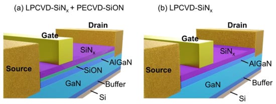
Figure 1.
Schematics of MIS-HEMTs with (a) SiNx/SiON and (b) SiNx gate dielectric. The gate-to-source distance (Lgs), gate-to-drain distance (Lgd), gate length (Lg), and gate width (Wg) were 2 μm, 14 μm, 2 μm, and 100 μm, respectively.
3. Results and Discussion
The electrical characteristics of the MIS-HEMTs were measured by Keysight B1505A, including DC characterization, interface state, and threshold voltage (Vth) stability under different gate voltage sweeping ranges. The transfer characteristics of the two samples under various gate-source voltage (Vgs) sweep ranges are shown in Figure 2. During the sequential sweeps, the gate voltage was scanned from −15 V to a maximum gate voltage (Vmax). To investigate the effects of the gate voltage stress, the Vmax was changed manually for each scan from −6 V to 12 V with a step of 2 V, where the drain−source voltage (Vds) was fixed at 1 V. The stress time of the Vmax was < 1 s. With the increase in Vmax, the Vth of the MIS-HEMT with SiNx/SiON composite gate dielectric varied from −9.49 V to −8.68 V with a variation (∆Vth) of 0.81 V. The Vth of the MIS-HEMT with SiNx only gate dielectric varied from −5.01 V to −3.24 V with a much larger ∆Vth of 1.77 V. It indicates that the maximum gate voltage stress affects the following transfer curves with a positive shift of Vth and the SiNx/SiON composite gate dielectric can significantly improve the Vth stability of the GaN MIS-HEMTs.
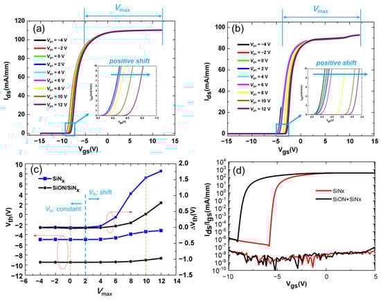
Figure 2.
Transfer characteristics of AlGaN/GaN MIS-HEMTs with (a) SiNx/SiON dual layers and (b) SiNx layer under various gate-source voltage sweeps. (c) The threshold voltage (Vth) and the Vth hysteresis (∆Vth) as a function of gate voltage stress (Vmax). (d) Gate leakage comparison.
The Vth and the Vth hysteresis (∆Vth) of MIS-HEMTs as a function of the Vmax are summarized in Figure 2c. The ∆Vth was defined as the Vth difference between the Vth with a scanned Vmax and the Vth with a Vmax of −6 V. The Vth of the MIS-HEMT with SiNx/SiON gate dielectric was almost constant as Vmax changed from −4 V to 12 V, whereas there was an obvious positive shift of the Vth for the MIS-HEMT with SiNx only gate dielectric. The ∆Vth of both kinds of MIS-HEMTs were almost 0 V as the Vmax increased from −4 V to 4 V and increased as the Vmax increased further. The ∆Vth of the MIS-HEMT with SiNx/SiON and SiNx only gate dielectric at Vmax = 12 V were 0.81 V and 1.77 V, respectively. Therefore, the SiNx/SiON composite gate dielectric can effectively improve the stability of the threshold voltage and reduce the threshold voltage hysteresis compared with SiNx only gate dielectric. The positive shift of the Vth at Vmax > 2 V indicates a trapping process of electrons by the interface states between the dielectric layer and the barrier layer, or the acceptor-like traps in the barrier layer [10,29] thereby requiring a higher Vth for ON-state. Figure 2d shows the comparison of the gate leakage for the two kinds of devices. Although the total thicknesses of the dielectrics are different, the devices showed almost the same gate leakage suggesting a high quality of the LPCVD-SiNx layer as designed for reducing the gate leakage current.
The influences of the OFF-state stress was also investigated to further compare the performance of the two kinds of devices as shown in Figure 3. The transfer curves of the MIS-HEMTs were first measured Vmax = 10 V (shift region as shown in Figure 2c). Then, the devices were stressed by an OFF-state condition with Vgs of −10 V and Vds = 1 V for 200 s. The transfer curves of the MIS-HEMTs after the OFF-state stress were measured with Vmax = 10 V for comparison. The transfer curves with Vmax = 0 V (constant region as shown in Figure 2c) are also shown in Figure 3 as references. The Vth of the MIS-HEMT with SiNx/SiON composite gate dielectric exhibited a negative shift of 0.5 V, whereas the Vth of the MIS-HEMT with SiNx only gate dielectric showed a negative shift of 0.62 V. The negative shift after the OFF-state stress indicates an electron releasing process from the traps to the 2DEG channel resulting in the recovery of the Vth [12].
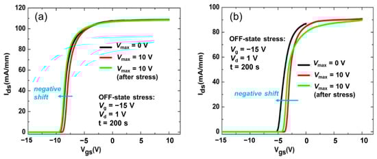
Figure 3.
Transfer characteristics of the MIS-HEMTs with (a) SiNx/SiON dual layers and (b) SiNx layer before (black and red) and after OFF-state stress (green).
To clarify the trapping and detrapping process causing the shift of the Vth, the band diagrams of the MIS-HEMTs at the gate region are depicted in Figure 4 [30]. At thermal equilibrium, traps at the interface below the Fermi level are filled with electrons, whereas traps above the Fermi level are empty [19]. When Vgs > Vth, the Fermi level of the interface states shifts upwards resulting in more empty traps below the Fermi level. Then, the traps below the Fermi level will be filled by electrons from the channel, i.e., the electron trapping process, as shown in Figure 4a. The higher the Vmax is applied to the gate, the more the electrons are trapped by the interface states, as shown in Figure 4b. This process causes the positive shift of the Vth. When the OFF-state condition or the negative gate bias is applied, the Fermi level shifts downwards resulting in the detrapping process of electrons back to the 2DEG channel, as shown in Figure 4c [31]. This process causes the negative shift of the Vth.
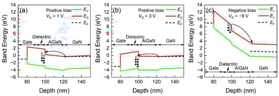
Figure 4.
Schematic band diagrams of MIS-HEMTs at (a) positive bias (Vmax = 1 V), (b) positive bias (Vmax = 3 V), and (c) negative bias (Vgs = −9 V).
Capacitance method was used to evaluate the interface states [32]. Figure 5a,b show the C-V curves of the two kinds of MIS-HEMTs at different frequencies from 100 kHz to 1 kHz. There are two steps in the C-V curves. The first one corresponds to the 2DEG accumulation at the AlGaN/GaN interface. The second one corresponds to that at the dielectric/AlGaN interface. The interface state density can be estimated based on the frequency dispersions of the second slope onset. The detailed calculation formula can be found in [14]. The interface state density distributions as a function of energy level are presented in Figure 5c. At the energy level of 0.36 eV~0.47 eV, the interface state density of the MIS-HEMT with SiNx/SiON composite gate dielectric was on the order of ~1013, which is significantly smaller than that of the MIS-HEMT with SiNx only. Compared with the SiNx only dielectric, SiNx/SiON can effectively reduce the overall interface states density, especially at deep energy levels. These results further prove that the SiNx/SiON composite gate dielectric in this work can considerably reduce the interface state density thereby improving the electrical performance of the GaN-based MIS-HEMTs. The thicknesses of SiNx and SiON extracted from the C-V profiles are 20.3 nm and 9.6 nm, respectively, which are consistent with the designed values. The output curves are shown in Figure 5d. The on-resistance for the MIS-HEMTs with SiNx/SiON composite gate dielectric and SiNx only gate dielectric is 3.12 mΩ·cm2 and 3.4 mΩ·cm2, respectively.
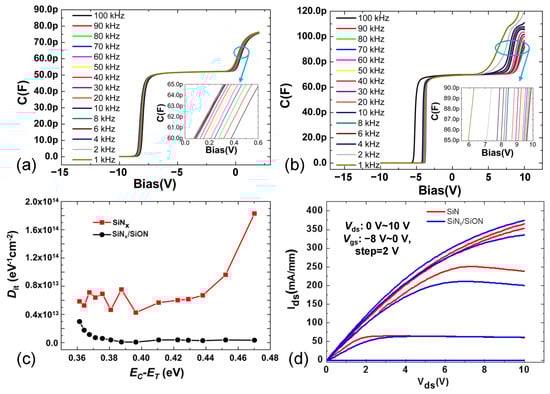
Figure 5.
C-V curves of AlGaN/GaN MISHEMTs with (a) Si3N4/SiON composite gate dielectrics and (b) SiNx gate dielectric. (c) The interface state density as a function of energy level for the AlGaN/GaN MIS-HEMTs with different gate dielectrics. (d) Output curves of the two kinds of devices.
4. Conclusions
AlGaN/GaN MIS-HEMTs on Si with SiNx/SiON composite gate dielectric were demonstrated. Low-temperature PECVD-SiON can improve the contact interface between GaN and the dielectric layer, and suppress the high thermal decomposition of GaN surface during the LPCVD-SiNx process. High-quality LPCVD-SiNx can serve as an excellent gate dielectric to enhance device performance. Compared with the MIS-HEMT with only LPCVD-SiNx, the device with the SiNx/SiON composite gate dielectric showed more stable Vth and much smaller ∆Vth. Frequency-dependent C-V measurements showed that the device with the composite dielectric had a significantly smaller interface state density. This work shows a route to realizing high-performance GaN-based MIS-HEMTs with a SiNx/SiON composite gate dielectric layer.
Author Contributions
Conceptualization, X.Z. and P.Z.; methodology, X.W.and K.F.; validation, X.W. and H.Z.; formal analysis, L.Z. and G.Y.; investigation, X.D. and Y.F.; resources, X.Z. and Z.D.; data curation, X.Z. and H.F.; writing—original draft preparation, X.Z. and P.Z.; writing—review and editing, X.Z. and K.F.; supervision, Y.C. and B.Z.; project administration, X.Z. All authors have read and agreed to the published version of the manuscript.
Funding
This research was funded by National Natural Science Foundation of China, grant number U1830112 and Natural Science Foundation of Jiangsu Province, China, grant No. BK20191195.
Data Availability Statement
The data presented in this study are available on request from the first author.
Acknowledgments
The authors would like to thank the Nano Fabrication Facility, Platform for Characterization and Test, Vacuum Interconnected Nanotech Workstation (NANO-X) of Suzhou Institute of Nano-Tech and Nano-Bionics, Chinese Academy of Sciences.
Conflicts of Interest
The authors declare no conflict of interest.
References
- Baliga, B.J. Gallium nitride devices for power electronic applications. Semicond. Sci. Technol. 2013, 28, 074011. [Google Scholar] [CrossRef]
- Fu, H.; Fu, K.; Yang, C.; Liu, H.; Hatch, K.A.; Peri, P.; Mudiyanselage, D.H.; Li, B.; Kim, T.-H.; Alugubelli, S.R.; et al. Selective area regrowth and doping for vertical gallium nitride power devices: Materials challenges and recent progress. Mater. Today 2021, 49, 296–323. [Google Scholar] [CrossRef]
- Chen, K.J.; Häberlen, O.; Lidow, A.; Lin Tsai, C.; Ueda, T.; Uemoto, Y.; Wu, Y. GaN-on-Si power technology: Devices and applica-tions. IEEE Trans. Electron Devices 2017, 64, 779–795. [Google Scholar] [CrossRef]
- Ikeda, N.; Niiyama, Y.; Kambayashi, H.; Sato, Y.; Nomura, T.; Kato, S.; Yoshida, S. GaN Power Transistors on Si Substrates for Switching Applications. Proc. IEEE 2010, 98, 1151–1161. [Google Scholar] [CrossRef]
- Hao, R.; Sun, C.; Fang, B.; Xu, N.; Tao, Z.; Zhang, H.; Wei, X.; Lin, W.; Zhang, X.; Yu, G.; et al. Monolithic integration of en-hancement/depletion-mode high electron mobility transistors using hydrogen plasma treatment. Appl. Phys. Express 2019, 12, 036502. [Google Scholar] [CrossRef]
- Hashizume, T.; Nishiguchi, K.; Kaneki, S.; Kuzmik, J.; Yatabe, Z. State of the art on gate insulation and surface passivation for GaN-based power HEMTs. Mater. Sci. Semicond. Processing 2018, 78, 85–95. [Google Scholar] [CrossRef]
- Fu, K.; Fu, H.; Huang, X.; Yang, T.H.; Chen, H.; Baranowski, I.; Montes, J.; Yang, C.; Zhou, J.; Zhao, Y. Threshold switching and memory behaviors of epitaxially regrown GaN-on-GaN vertical p-ndiodes with high temperature stability. IEEE Electron Device Lett. 2019, 40, 375. [Google Scholar] [CrossRef]
- Lagger, P.; Ostermaier, C.; Pobegen, G.; Pogany, D. Towards understanding the origin of threshold voltage instability of AlGaN/GaN MIS-HEMTs. In Proceedings of the IEEE International Electron Devices Meeting (IEDM), San Francisco, CA, USA, 10–13 December 2012; pp. 13.1.1–13.1.4. [Google Scholar]
- Asubar, J.T.; Yatabe, Z.; Gregusova, D.; Hashizume, T. Controlling surface/interface states in GaN-based transistors: Surface model insulated gate and surface passivation. J. Appl. Phys. 2021, 129, 121102. [Google Scholar] [CrossRef]
- Joshi, V.; Gupta, S.D.; Chaudhuri, R.R.; Shrivastava, M. Physical Insights Into the Impact of Surface Traps on Breakdown Char-acteristics of AlGaN/GaN HEMTs—Part I. IEEE Trans. Electron Devices 2021, 68, 72–79. [Google Scholar] [CrossRef]
- Arulkumaran, S.; Egawa, T.; Ishikawa, H.; Jimbo, T.; Sano, Y. Surface passivation effects on AlGaN/GaN high-electron-mobility transistors with SiO2, Si3N4, and silicon oxynitride. Appl. Phys. Lett. 2004, 84, 613. [Google Scholar] [CrossRef]
- Zhang, Z.; Li, W.; Fu, K.; Yu, G.; Zhang, X.; Zhao, Y. AlGaN/GaN MIS-HEMTs of Very Low Vth Hysteresis and Current Collapse with In-Situ Pre-Deposition Plasma Nitridation and LPCVD-Si3N4 Gate Insulator. IEEE Electron Device Lett. 2017, 38, 2. [Google Scholar] [CrossRef]
- Sun, Z.; Cheng, W.; Gao, J.; Liang, H.; Huang, H.; Wang, R.; Sun, N.; Tao, P.; Ren, Y.; Song, S.; et al. Improving Performances of Enhancement-Mode AlGaN/GaN MIS-HEMTs on 6-inch Si Substrate Utilizing SiON/Al2O3 Stack Dielectrics. IEEE Electron Device Lett. 2020, 41, 135–138. [Google Scholar] [CrossRef]
- Kim, H.S.; Han, S.W.; Jang, W.H.; Cho, C.H.; Seo, K.S.; Oh, J.; Cha, H.Y. Normally-off GaN-on-Si MISFET using PECVD SiON gate dielectric. IEEE Electron Device Lett. 2017, 38, 1090–1093. [Google Scholar] [CrossRef]
- Dutta, G.; DasGupta, N.; DasGupta, A. Effect of Sputtered-Al2O3 Layer Thickness on the Threshold Voltage of III-Nitride MIS-HEMTs. IEEE Trans. Electron Devices 2016, 63, 4. [Google Scholar] [CrossRef]
- Sun, X.; Saadat, O.I.; Chang-Liao, K.S.; Palacios, T.; Cui, S.; Ma, T.P. Study of gate oxide traps in HfO2/AlGaN/GaN met-al-oxide-semiconductor high-electron-mobility transistors by use of ac transconductance method. Appl. Phys. Lett. 2013, 102, 103504. [Google Scholar] [CrossRef] [Green Version]
- Cui, P.; Zhang, J.; Jia, M.; Lin, G.; Wei, L.; Zhao, H.; Gundlach, L.; Zeng, Y. InAlN/GaN metal–insulator–semiconductor high-electron-mobility transistor with plasma enhanced atomic layer-deposited ZrO2 as gate dielectric. Jpn. J. Appl. Phys. 2020, 59, 020901. [Google Scholar] [CrossRef]
- Yang, T.-H.; Brown, J.; Fu, K.; Zhou, J.; Hatch, K.; Yang, C.; Montes, J.; Qi, X.; Fu, H.; Nemanich, R.J.; et al. AlGaN/GaN metal–insulator–semiconductor high electron mobility transistors (MISHEMTs) using plasma deposited BN as gate dielectric. Appl. Phys. Lett. 2021, 118, 072102. [Google Scholar] [CrossRef]
- Zhang, Z.; Yu, G.; Zhang, X.; Deng, X.; Li, S.; Fan, Y.; Sun, S.; Song, L.; Tan, S.; Wu, D.; et al. Studies on High Voltage GaN-on-Si MIS-HEMTs Using LPCVD-Si3N4 as Gate Dielectric and Passivation Layer, Electron Devices. IEEE Trans. Electron Devices 2015, 63, 731–738. [Google Scholar] [CrossRef]
- Rzin, M.; Guillet, B.; Mechin, L.; Gamarra, P.; Lacam, C.; Medjdoub, F.; Routoure, J.-M. Routoure, Impact of the in situ SiN Thickness on Low-Frequency Noise in MOVPE InAlGaN/GaN HEMTs. IEEE Trans. Electron Devices 2019, 66, 5080–5083. [Google Scholar] [CrossRef]
- Roccaforte, F.; Fiorenza, P.; Greco, G.; Nigro, R.L.; Giannazzo, F.; Iucolano, F.; Saggio, M. Emerging trends in wide band gap sem-iconductors (SiC and GaN) technology for power devices. Microelectron. Eng. 2018, 187–188, 66–77. [Google Scholar] [CrossRef]
- Zeng, F.; An, J.X.; Zhou, G.; Li, W.; Wang, H.; Duan, T.; Jiang, L.; Yu, H. A Comprehensive Review of Recent Progress on GaN High Electron Mobility Transistors: Devices, Fabrication and Reliability. Electronics 2018, 7, 377. [Google Scholar] [CrossRef] [Green Version]
- Hua, M.; Zhang, Z.; Wei, J.; Lei, J.; Tang, G.; Fu, K.; Cai, Y.; Zhang, B.; Chen, K.J. Integration of LPCVD-SiNx gate dielectric with recessed-gate E-mode GaN MIS-FETs: Toward high performance, high stability and long TDDB lifetime. In Proceedings of the IEEE International Electron Devices Meeting (IEDM), San Francisco, CA, USA, 3–7 December 2016; pp. 260–263. [Google Scholar]
- Nishio, K.; Yayama, T.; Miyazaki, T.; Taoka, N.; Shimizu, M. Ultrathin silicon oxynitride layer on GaN for dangling-bond-free GaN/insulator interface. Sci. Rep. 2018, 8, 1391. [Google Scholar] [CrossRef] [PubMed] [Green Version]
- Long, R.D.; McIntyre, P.C. Surface Preparation and Deposited Gate Oxides for Gallium Nitride Based Metal Oxide Semiconductor Devices. Materials 2012, 5, 1297–1335. [Google Scholar] [CrossRef]
- Cheng, K.-Y.; Wu, S.-C.; Yu, C.-J.; Wang, T.-W.; Liao, J.-H.; Wu, M.-C. Comparative study on performance of AlGaN/GaN MS-HEMTs with SiNx, SiOx, and SiNO surface passivation. Solid-State Electron. 2020, 170, 107824. [Google Scholar] [CrossRef]
- Geng, K.; Chen, D.; Zhou, Q.; Wang, H. AlGaN/GaN MIS-HEMT with PECVD SiNx, SiON, SiO2 as Gate Dielectric and Passivation Layer. Electronics 2018, 7, 416. [Google Scholar] [CrossRef] [Green Version]
- Zhang, Z.; Song, L.; Li, W.; Fu, K.; Yu, G.; Zhang, X.; Fan, Y.; Deng, X.; Li, S.; Sun, S.; et al. Mechanism of leakage of ion-implantation isolated AlGaN/GaN MIS-high electron mobility transistors on Si substrate. Solid-State Electron. 2017, 134, 39–45. [Google Scholar] [CrossRef]
- Yamada, T.; Watanabe, K.; Nozaki, M.; Shih, H.-A.; Nakazawa, S.; Anda, Y.; Ueda, T.; Yoshigoe, A.; Hosoi, T.; Shimura, T.; et al. Physical and electrical characterizations of AlGaN/GaN MOS gate stacks with AlGaN surface oxidation treatment. Jpn. J. Appl. Phys. 2018, 57, 06KA07. [Google Scholar] [CrossRef] [Green Version]
- Yamada, H.; Yamada, T. A semiconductor physics based model for thermal characteristics in electronic electrolytic energy storage devices. J. Appl. Phys. 2021, 129, 174501. [Google Scholar] [CrossRef]
- Yamada, T.; Devine, E.P.; Ghandiparsi, S.; Bartolo-Perez, C.; Mayet, A.S.; Cansizoglu, H.; Gao, Y.; Ahamed, A.; Wang, S.-Y.; Islam, M.S. Modeling of nanohole silicon pin/nip photodetectors: Steady state and transient characteristics. Nanotechnology 2021, 32, 365201. [Google Scholar] [CrossRef]
- Yang, S.; Liu, S.; Lu, Y.; Liu, C.; Chen, K.J. AC-capacitance techniques for interface trap analysis in GaN-based buried-channel MIS-HEMTs. IEEE Trans. Electron Devices 2015, 62, 1870–1878. [Google Scholar] [CrossRef]
Publisher’s Note: MDPI stays neutral with regard to jurisdictional claims in published maps and institutional affiliations. |
© 2022 by the authors. Licensee MDPI, Basel, Switzerland. This article is an open access article distributed under the terms and conditions of the Creative Commons Attribution (CC BY) license (https://creativecommons.org/licenses/by/4.0/).