
Evaluation of the Long-Term Reliability of Open-Tube Diffused Planar InGaAs/InP Avalanche Photodiodes under a Hybrid of Thermal and Electrical Stresses


Abstract
:1. Introduction
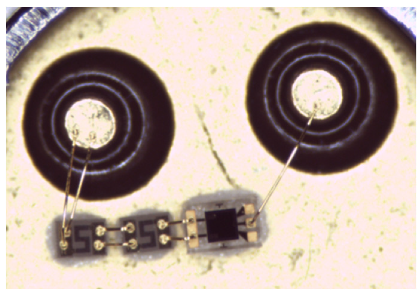
2. APD Test Structure Description
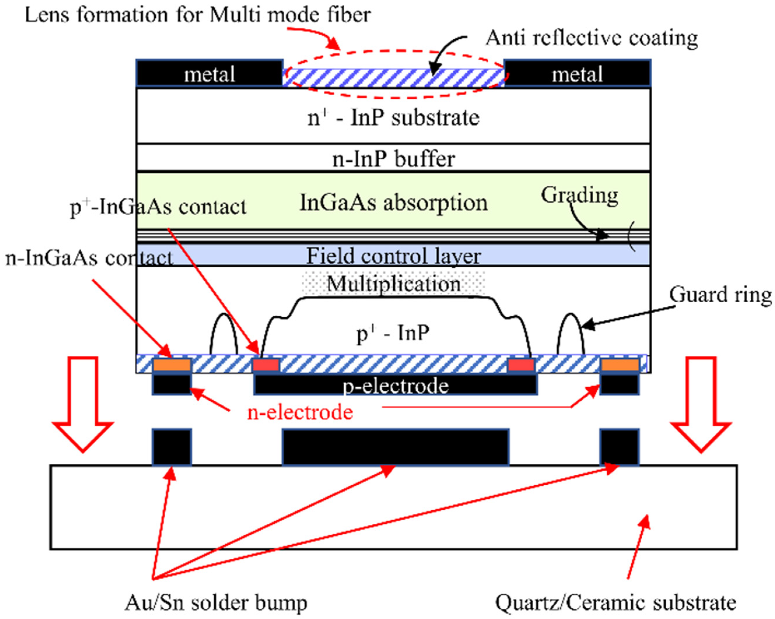
Design of APD Test Structure
3. Reliability Testing Experiments and Modeling Scheme
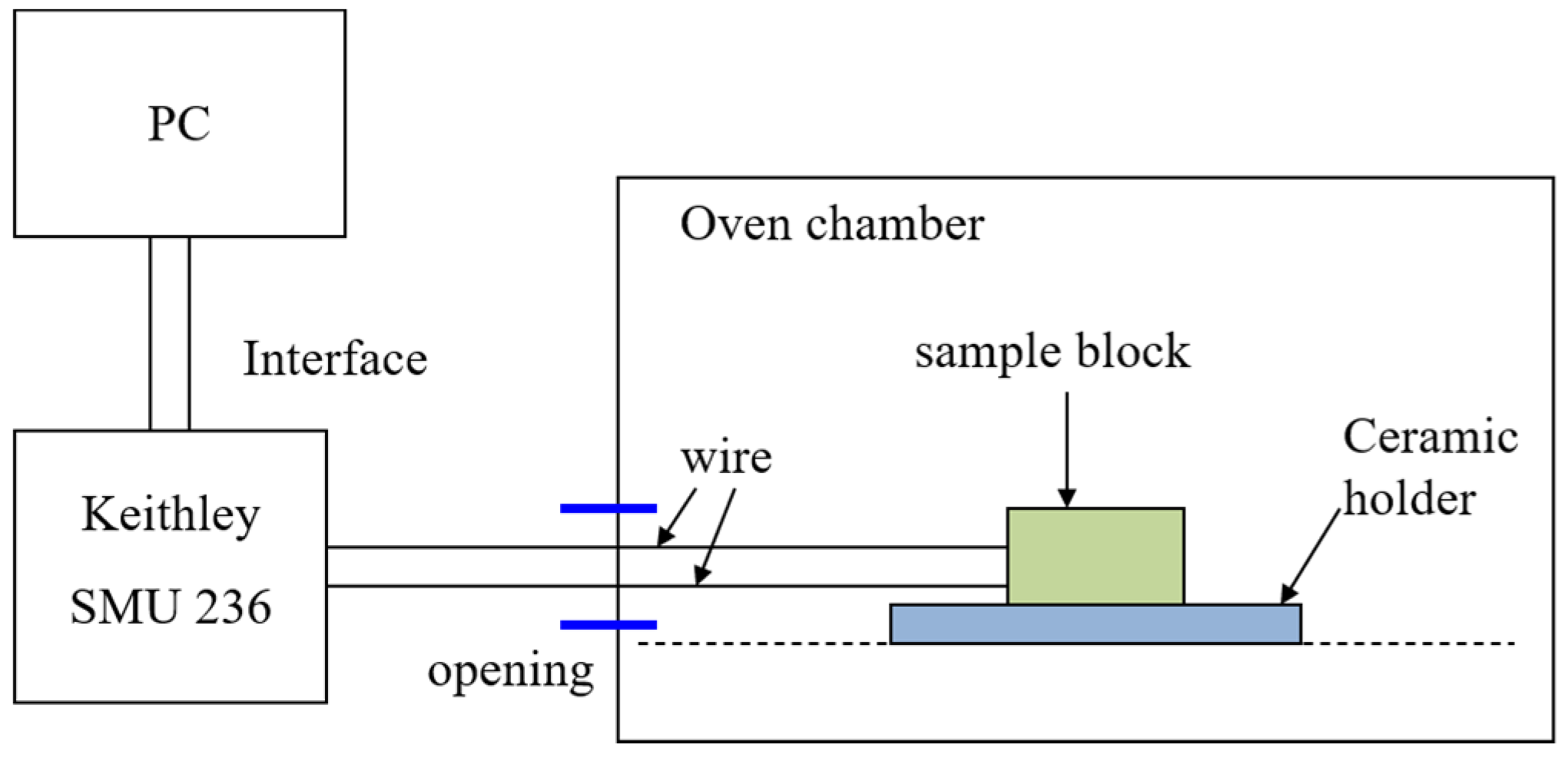
3.1. Device Reliability Experiments
3.2. Modeling Scheme
4. Results and Discussion
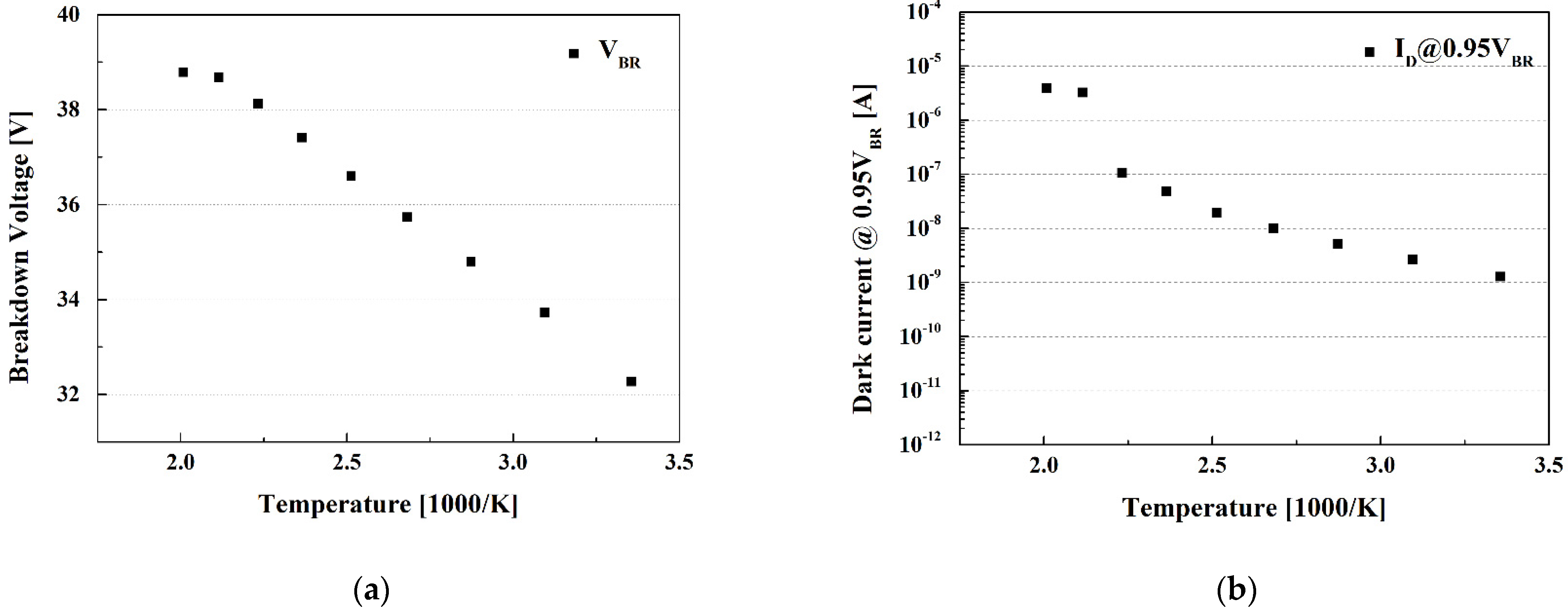
4.1. Initial Temperature-Dependent Electrical Characteristics
4.2. Results of the High-Temperature Storage Tests
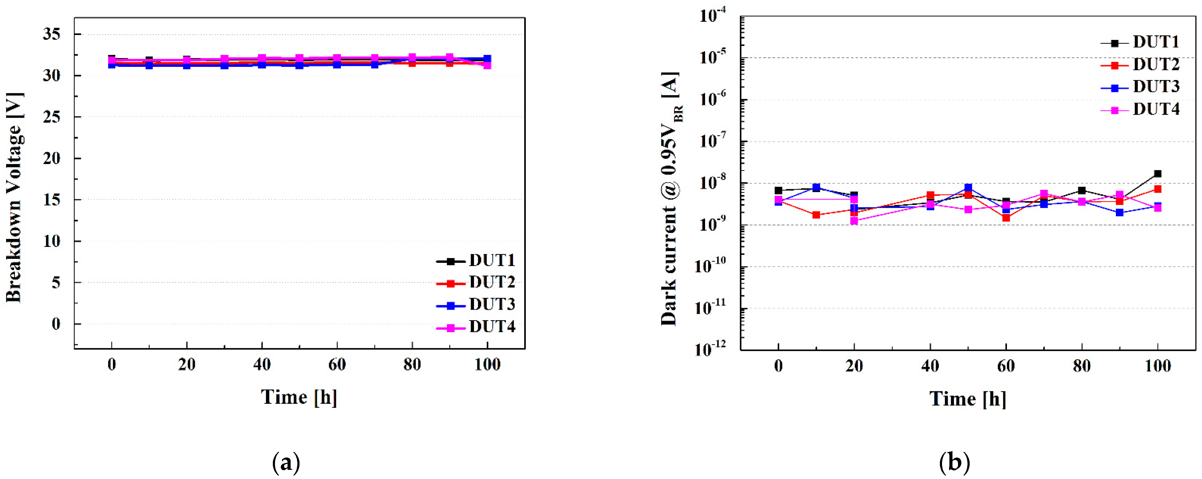
4.3. Pre-ALT Experiments
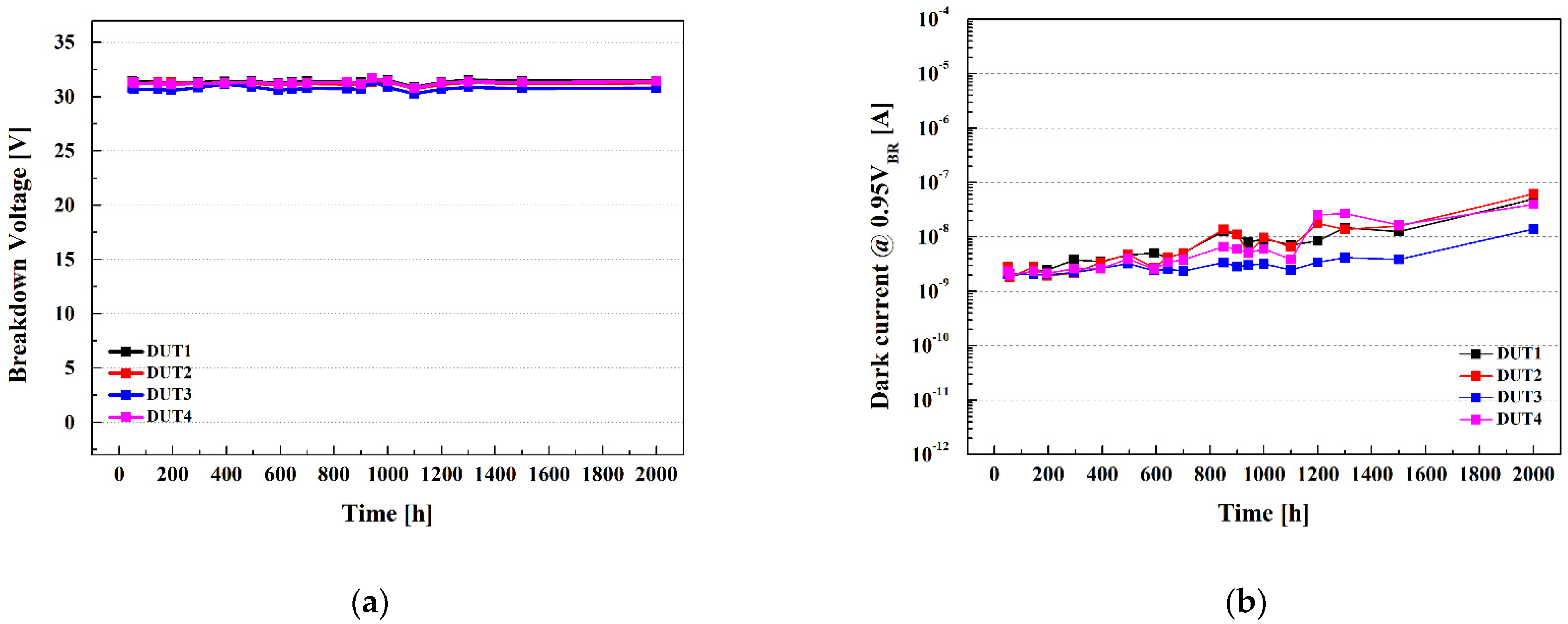
4.4. Accelerated Life Test Experiment Scheme
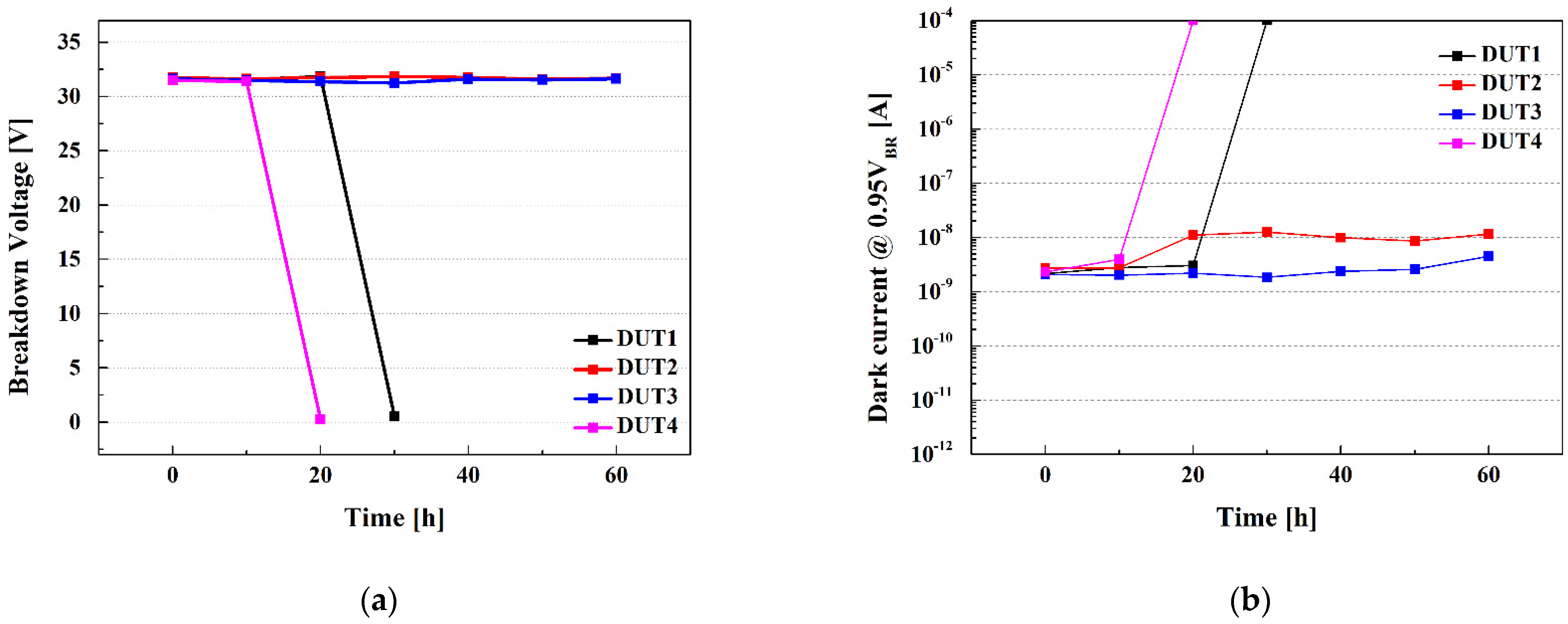
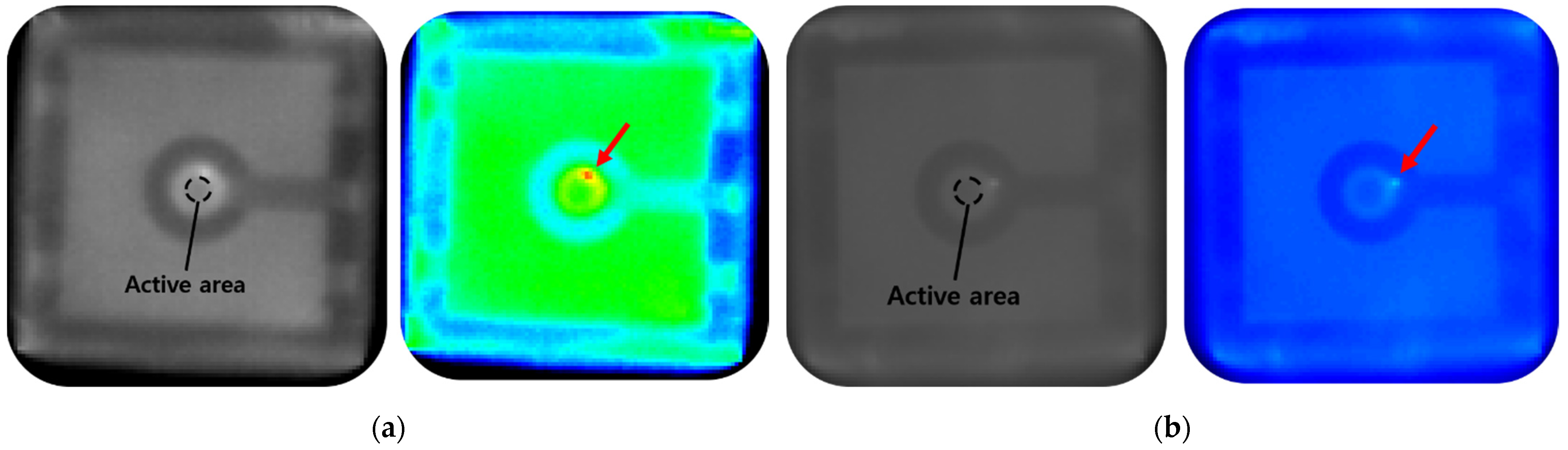
4.5. APD Failure Analysis
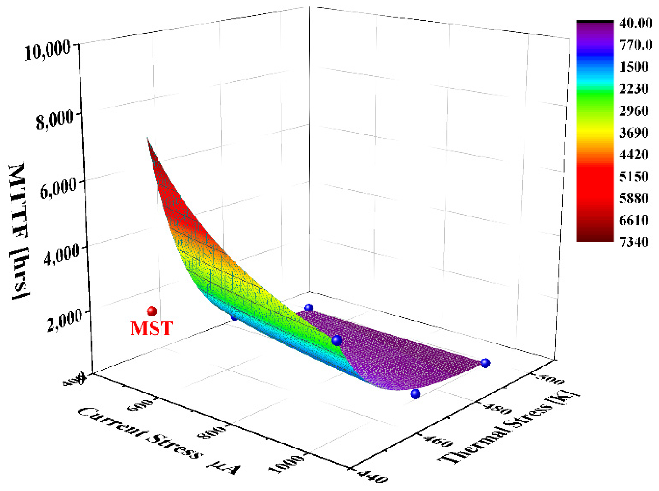
4.6. Extrapolation of Activation Energy and Estimate the APD Lifetime
5. Conclusions
Author Contributions
Funding
Acknowledgments
Conflicts of Interest
References
- Smetona, S.; Klunder, K.; An, S.; Rousina-Webb, R.; Emmerstorfer, B.; Jamroz, E.; Rouabhi, M.; Mallard, R. Reliability of InP-based avalanche photodiodes for high bit-rate fiber-optic communication systems. In Proceedings of the 14th Indium Phosphide and Related Materials Conference 2002 (Cat. No. 02CH37307), Stockholm, Sweden, 12–16 May 2002; IEEE: Piscataway, NJ, USA, 2002; pp. 373–376. [Google Scholar]
- Baek, S.H.; Yang, S.C.; Park, C.Y.; Park, C.W.; Cho, S.B.; Ryu, S.W. Room temperature quantum key distribution characteristics of low-noise InGaAs/InP single-photon avalanche diode. J. Korean Phys. Soc. 2021, 78, 634–641. [Google Scholar] [CrossRef]
- Yuan, Z.; Dixon, A.; Dynes, J.; Sharpe, A.; Shields, A. Gigahertz quantum key distribution with InGaAs avalanche photodiodes. Appl. Phys. Lett. 2008, 92, 201104. [Google Scholar] [CrossRef] [Green Version]
- Zhou, G.; Zhou, X.; Yang, J.; Tao, Y.; Nong, X.; Baysal, O. Flash Lidar sensor using fiber-coupled APDs. IEEE Sens. J. 2015, 15, 4758–4768. [Google Scholar] [CrossRef]
- Park, C.Y.; Kim, D.B.; Kim, C.H.; Kwon, Y.; Kang, E.C.; Lee, C.; Choi, S.G.; La, J.; Ko, J.S. Wideband receiver module for LADAR using large-area InGaAs avalanche photodiode. Korean J. Opt. Photonics 2013, 24, 1–8. [Google Scholar] [CrossRef] [Green Version]
- Charlamov, J.; Navickas, R.; Baskys, A.; Barzdenas, V.; Nickelson, L. Optical receiver for optical time domain reflectometer. Elektron. Ir Elektrotechnika 2012, 18, 49–52. [Google Scholar] [CrossRef]
- Choudhary, B.C. Optical Time Domain Reflectometry (OTDR). Available online: http://nitttrchd.ac.in/sitenew1/app_sc/ppts/fiber/OTDR&Applns.pdf (accessed on 1 March 2021).
- Liu, M.; Bai, X.; Hu, C.; Guo, X.; Campbell, J.C.; Pan, Z.; Tashima, M.M. Low dark count rate and high single-photon detection efficiency avalanche photodiode in Geiger-mode operation. IEEE Photonics Technol. Lett. 2007, 19, 378–380. [Google Scholar] [CrossRef]
- Liang, Y.; Chen, Y.; Huang, Z.; Bai, G.; Yu, M.; Zeng, H. Room-temperature single-photon detection with 1.5-GHz gated InGaAs/InP avalanche photodiode. IEEE Photonics Technol. Lett. 2016, 29, 142–145. [Google Scholar] [CrossRef]
- Liang, Y.; Wu, E.; Chen, X.; Ren, M.; Jian, Y.; Wu, G.; Zeng, H. Low-timing-jitter single-photon detection using 1-GHz sinusoidally gated InGaAs/InP avalanche photodiode. IEEE Photonics Technol. Lett. 2011, 23, 887–889. [Google Scholar] [CrossRef]
- Skrimshire, C.P.; Farr, J.R.; Sloan, D.F.; Robertson, M.J.; Putland, P.A.; Stokoe, J.C.D.; Sutherland, R.R. Reliability of mesa and planar InGaAs PIN photodiodes. IEEE Proc. J. Optoelectron. 1990, 137, 74–78. [Google Scholar] [CrossRef]
- Itzler, M.A.; Loi, K.; McCoy, S.; Codd, N.; Komaba, N. High-performance, manufacturable avalanche photodiodes for 10 Gb/s optical receivers. In Proceedings of the Optical Fiber Communication Conference, Baltimore, MD, USA, 7–10 March 2000; Optical Society of America: Washington, DC, USA, 2000; p. FG5. [Google Scholar]
- Jung, J.; Kwon, Y.H.; Hyun, K.S.; Yun, I. Reliability of planar InP-InGaAs avalanche photodiodes with recess etching. IEEE Photonics Technol. Lett. 2018, 14, 1160–1162. [Google Scholar] [CrossRef]
- Yun, I.; Menkara, H.M.; Wang, Y.; Oguzman, I.H.; Kolnik, J.; Brennan, K.F.; May, G.S.; Summers, C.J.; Wagner, B.K. Effect of doping on the reliability of GaAs multiple quantum well avalanche photodiodes. IEEE Trans. Electron Devices 1997, 44, 535–544. [Google Scholar]
- Yun, I.; May, G.S. Parametric manufacturing yield modeling of GaAs/AlGaAs multiple quantum well avalanche photodiodes. IEEE Trans. Semicond. Manuf. 1999, 12, 238–251. [Google Scholar]
- Lee, B.; Yun, I. Effect of different etching processes on edge breakdown suppression for planar InP/InGaAs avalanche photodiodes. Microelectron. J. 2002, 33, 645–649. [Google Scholar] [CrossRef]
- Jung, J.; Kwon, Y.H.; Hyun, K.S.; Yun, I. Reliability testing of single diffused planar InP/InGaAs avalanche photodiodes. In Proceedings of the 27th Annual IEEE/SEMI International Electronics Manufacturing Technology Symposium, San Jose, CA, USA, 17–18 July 2002; IEEE: Piscataway, NJ, USA, 2002; pp. 193–194. [Google Scholar]
- Yoon, K.H.; Shin, M.H.; Park, C.Y.; Yun, I.; Kim, S.J. Edge breakdown suppression of 10 Gbps avalanche photodiode. J. Korean Phys. Soc. 2005, 45, S936–S940. [Google Scholar]
- Petrosyants, K.O.; Kharitonov, I.A. Non-destructive testing of electronic components overheating using infrared thermography. In Proceedings of the VIII International Workshop on Non-Destructive Tests, Prague, Czech Republic, 12–14 October 2015; pp. 127–131. [Google Scholar]


| Parameter | Measured Condition | Criterion of Failure |
|---|---|---|
| VBR | @ 10 μA | ΔVBR > ±10% |
| ID | @ 0.95 VBR | ID > 1 μA |
| Temperature (K) | Current (μA) | Number of Samples | Note |
|---|---|---|---|
| 498 | - | 4 | HTST |
| 498 | 100 | 4 | Preliminary ALT experiments |
| 448 | 500 | 4 | |
| 448 | 1000 | 4 | |
| 473 | 500 | 8 | Main ALT experiments |
| 473 | 1000 | 8 | |
| 498 | 500 | 8 | |
| 498 | 1000 | 13 |
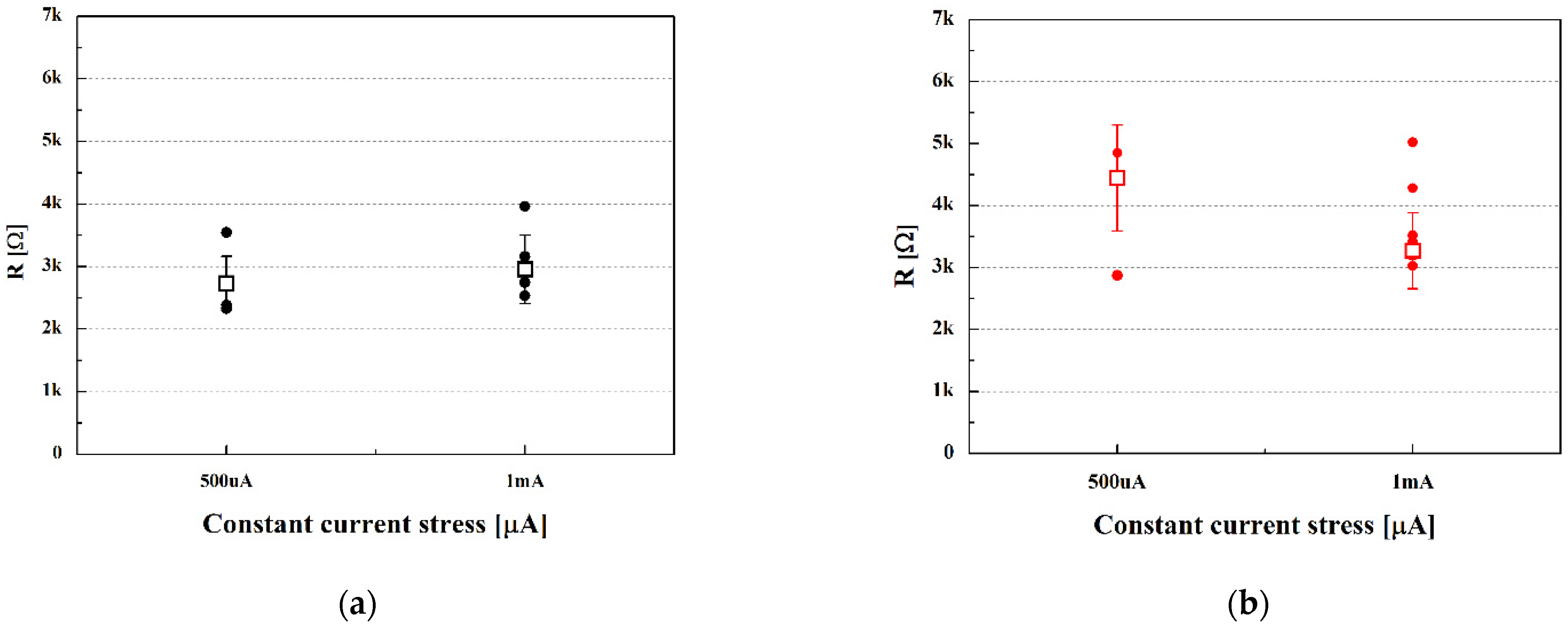
| Temperature (K) | Current (μA) | Median Resistance (kΩ) | Standard Deviation (Ω) |
|---|---|---|---|
| 473 | 500 | 2.73 | 434 |
| 473 | 1000 | 2.95 | 547 |
| 498 | 500 | 4.45 | 853 |
| 498 | 1000 | 3.27 | 614 |
Publisher’s Note: MDPI stays neutral with regard to jurisdictional claims in published maps and institutional affiliations. |
© 2022 by the authors. Licensee MDPI, Basel, Switzerland. This article is an open access article distributed under the terms and conditions of the Creative Commons Attribution (CC BY) license (https://creativecommons.org/licenses/by/4.0/).
Share and Cite
Choi, H.; Park, C.-Y.; Baek, S.-H.; Moon, G.Y.; Yun, I. Evaluation of the Long-Term Reliability of Open-Tube Diffused Planar InGaAs/InP Avalanche Photodiodes under a Hybrid of Thermal and Electrical Stresses. Electronics 2022, 11, 802. https://doi.org/10.3390/electronics11050802
Choi H, Park C-Y, Baek S-H, Moon GY, Yun I. Evaluation of the Long-Term Reliability of Open-Tube Diffused Planar InGaAs/InP Avalanche Photodiodes under a Hybrid of Thermal and Electrical Stresses. Electronics. 2022; 11(5):802. https://doi.org/10.3390/electronics11050802
Chicago/Turabian StyleChoi, Hyejeong, Chan-Yong Park, Soo-Hyun Baek, Gap Yeal Moon, and Ilgu Yun. 2022. "Evaluation of the Long-Term Reliability of Open-Tube Diffused Planar InGaAs/InP Avalanche Photodiodes under a Hybrid of Thermal and Electrical Stresses" Electronics 11, no. 5: 802. https://doi.org/10.3390/electronics11050802
APA StyleChoi, H., Park, C.-Y., Baek, S.-H., Moon, G. Y., & Yun, I. (2022). Evaluation of the Long-Term Reliability of Open-Tube Diffused Planar InGaAs/InP Avalanche Photodiodes under a Hybrid of Thermal and Electrical Stresses. Electronics, 11(5), 802. https://doi.org/10.3390/electronics11050802