
Failure Analysis of Some Commercial Spotlights Based on Light Emitting Diodes


Abstract
1. Introduction
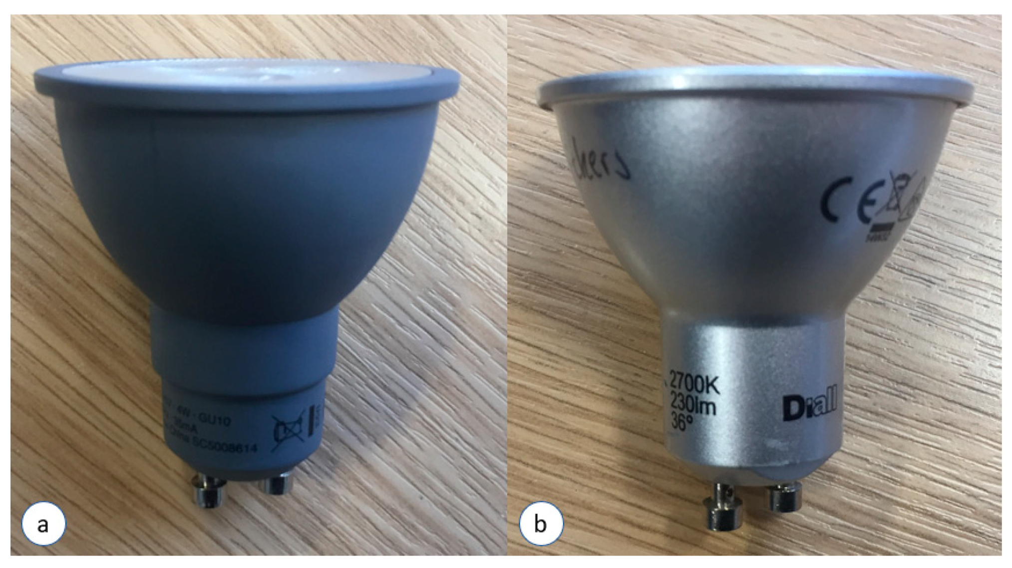
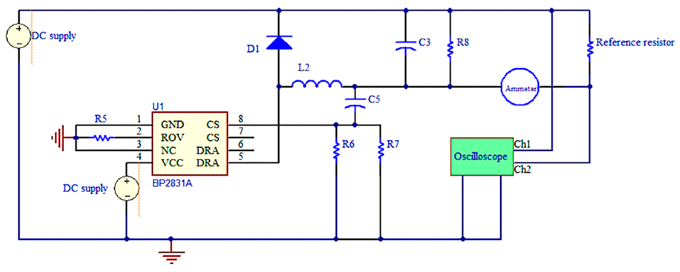
2. Methodology
3. Component Analysis
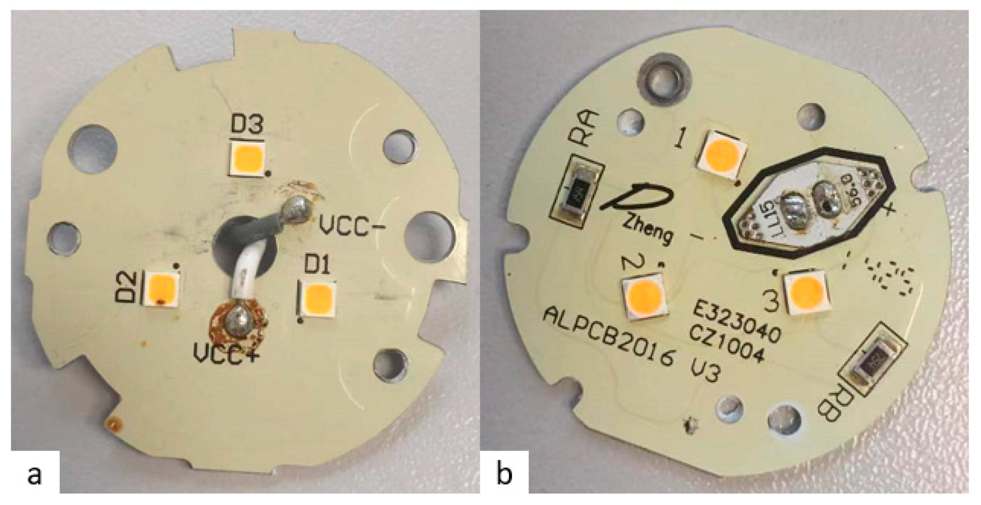
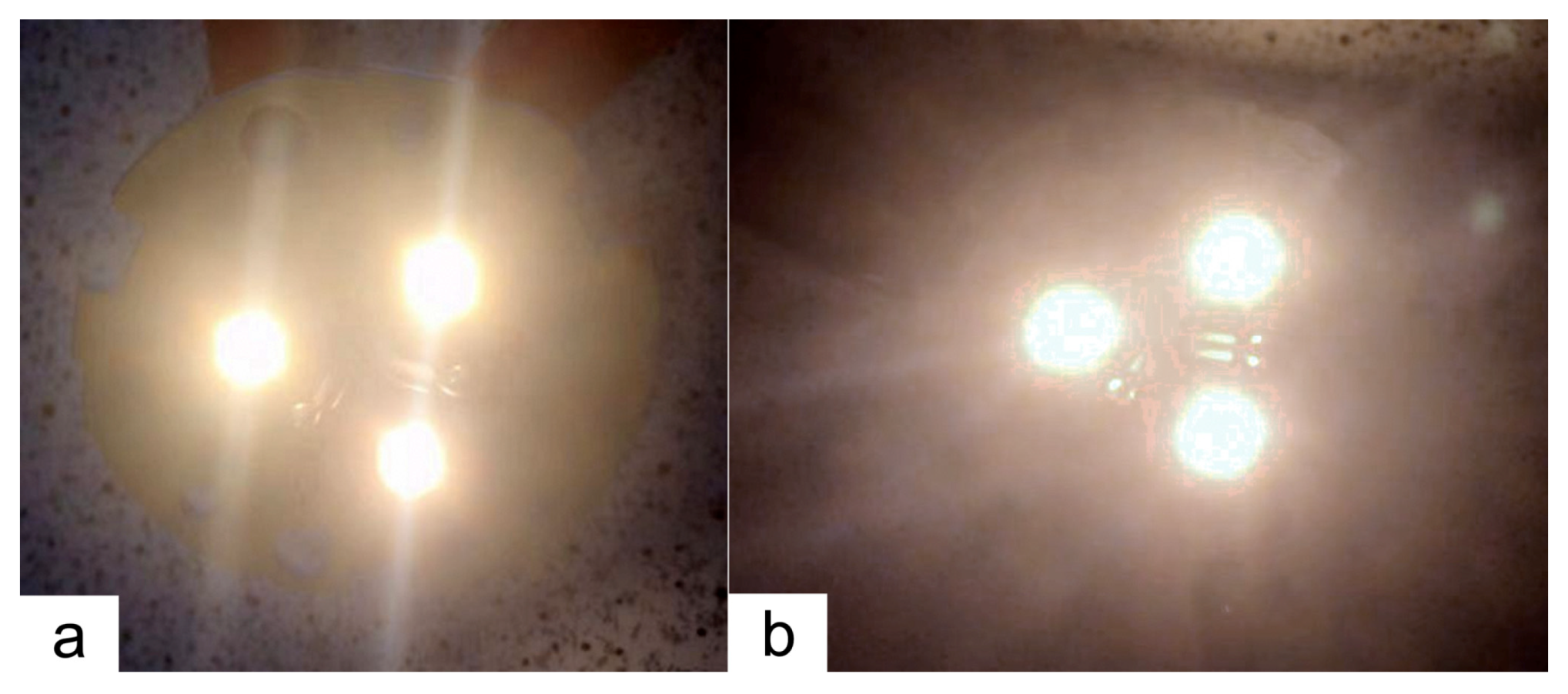
3.1. LED Heads
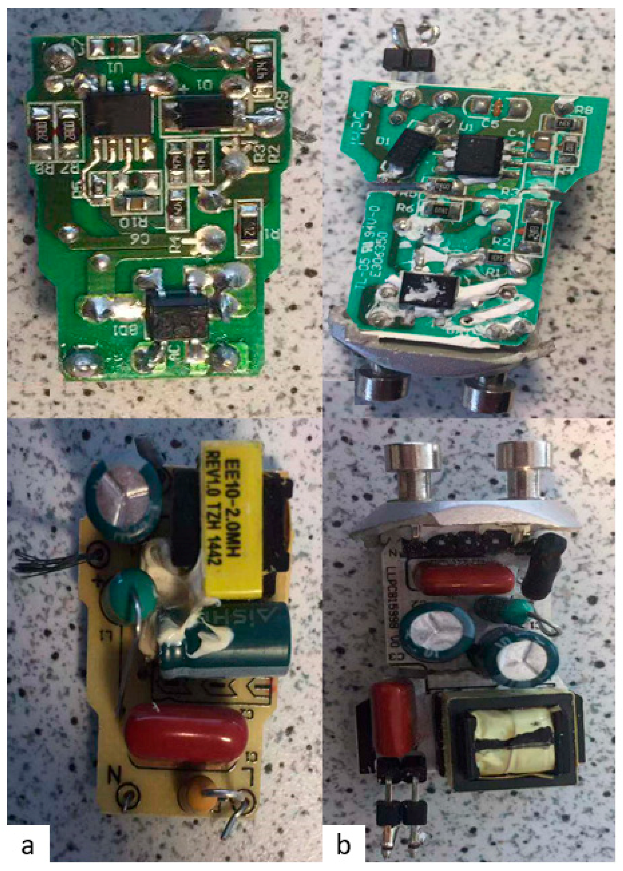
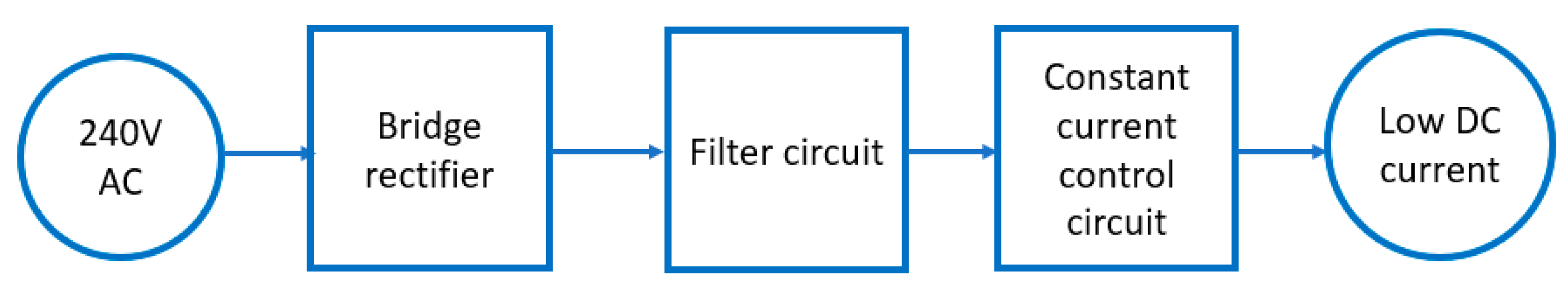
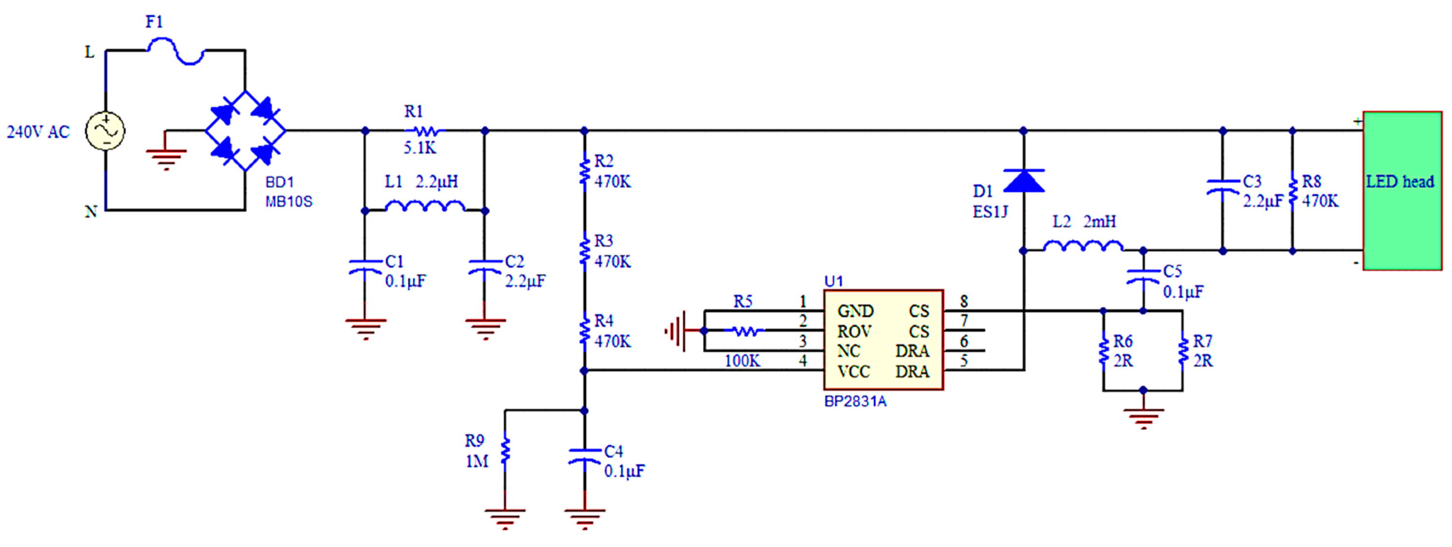
3.2. LED Drive Circuits
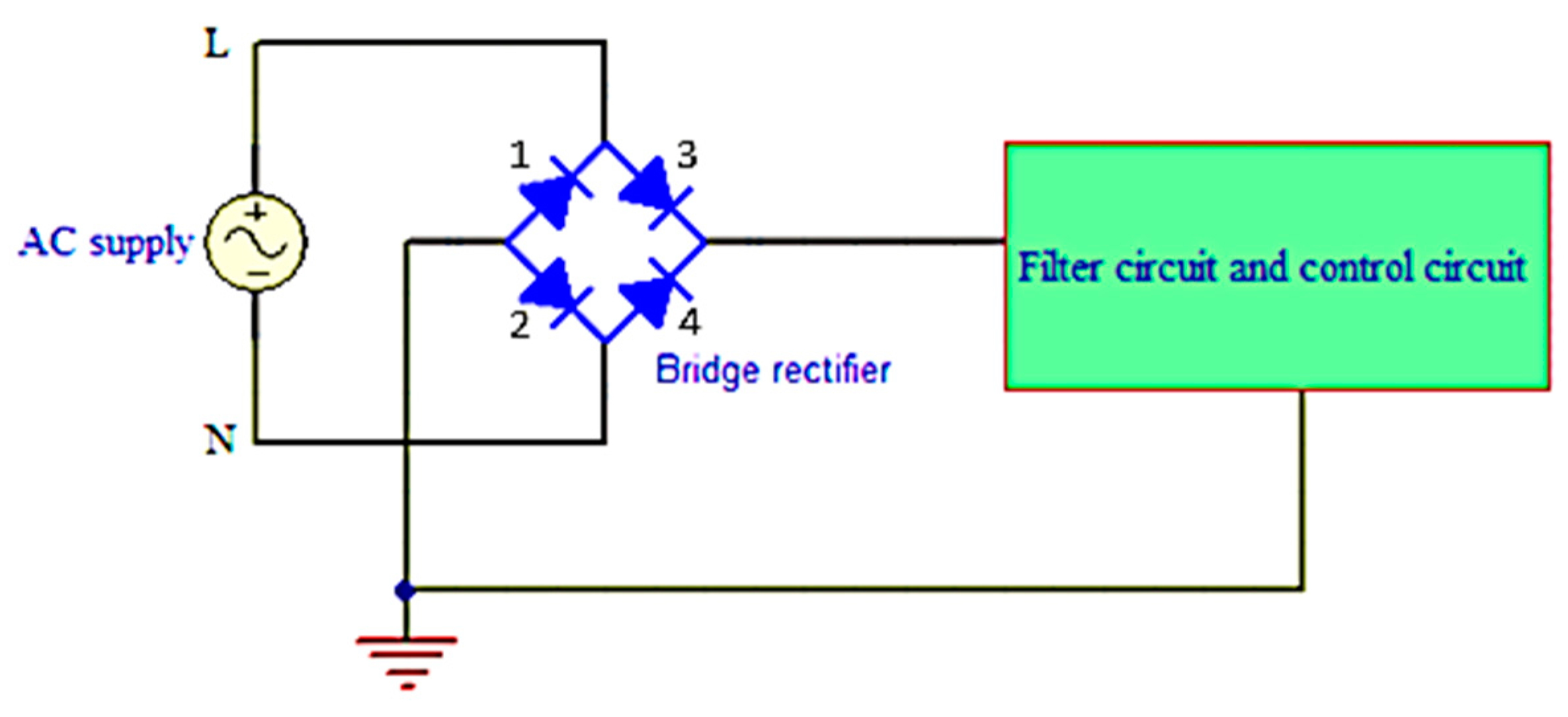
3.2.1. Bridge Rectifier
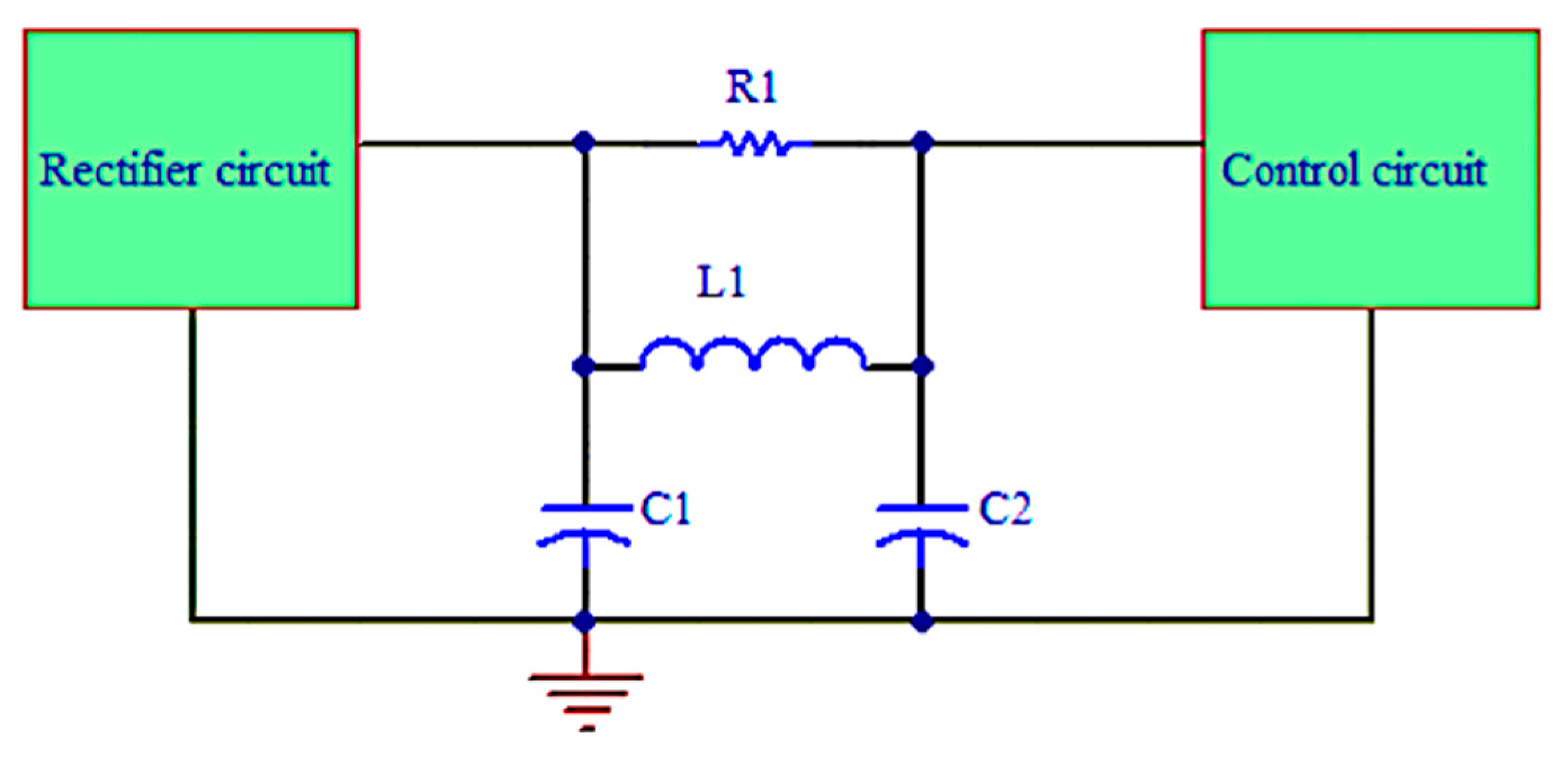
3.2.2. Filter Circuit
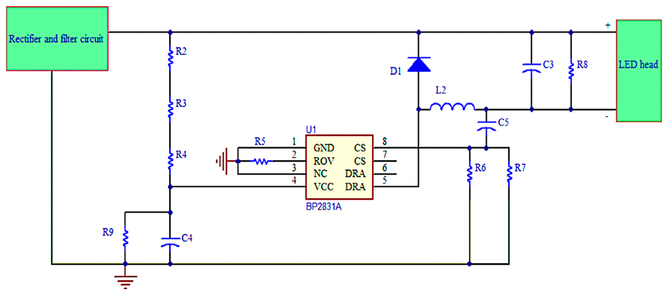
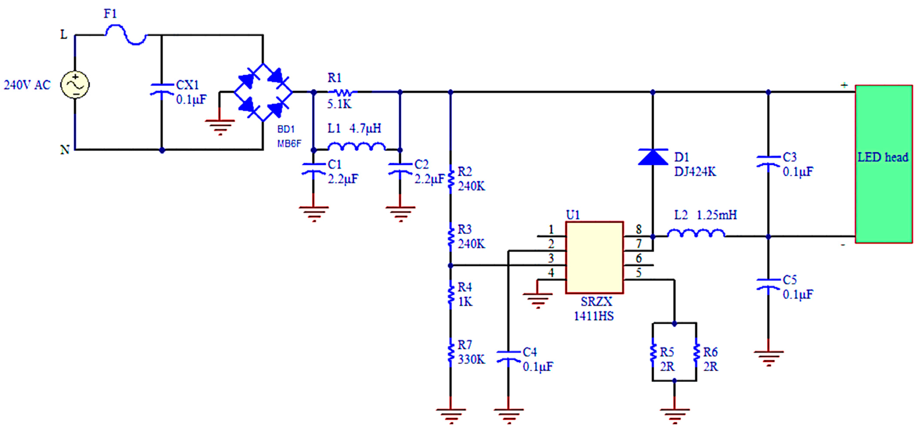
3.2.3. Control Circuit
4. Results and Evaluation
4.1. Analysis of Sample A Which Emits No Light
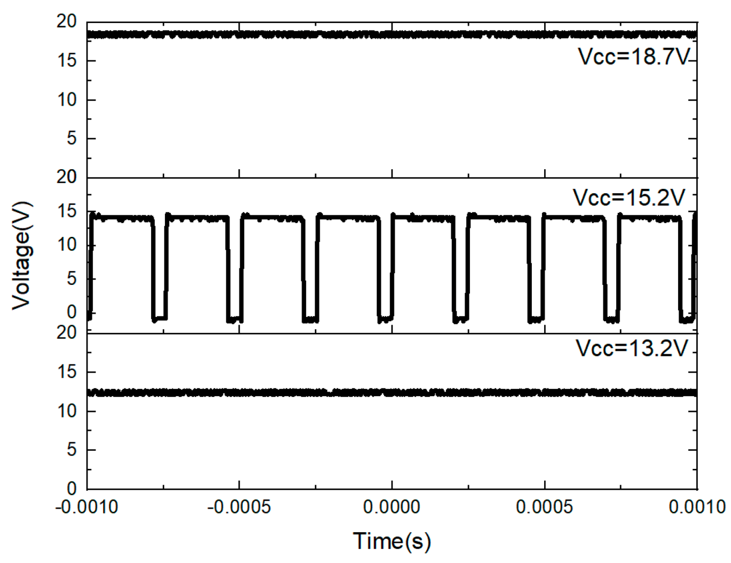
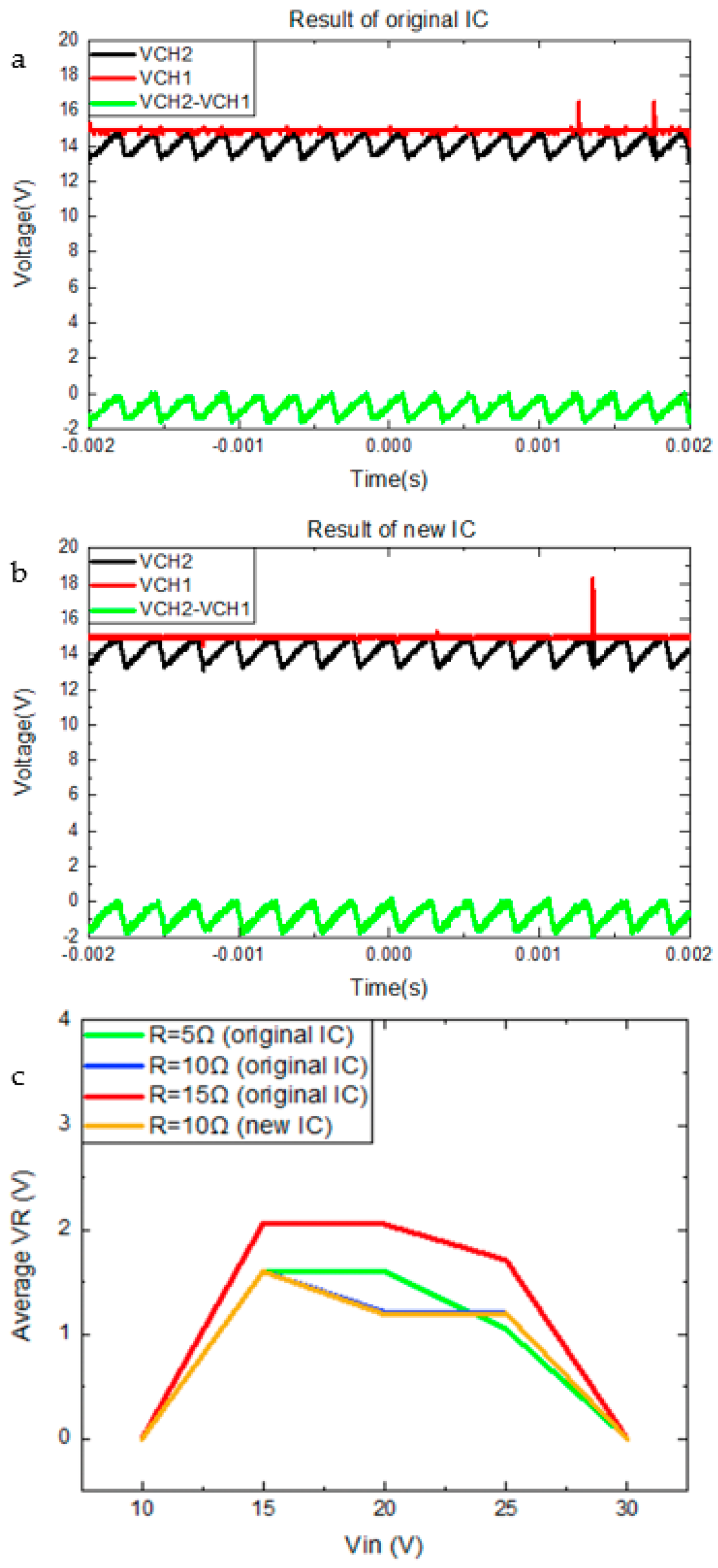
4.2. Analysis of Sample B That Showed Strong Flicker
5. Discussion
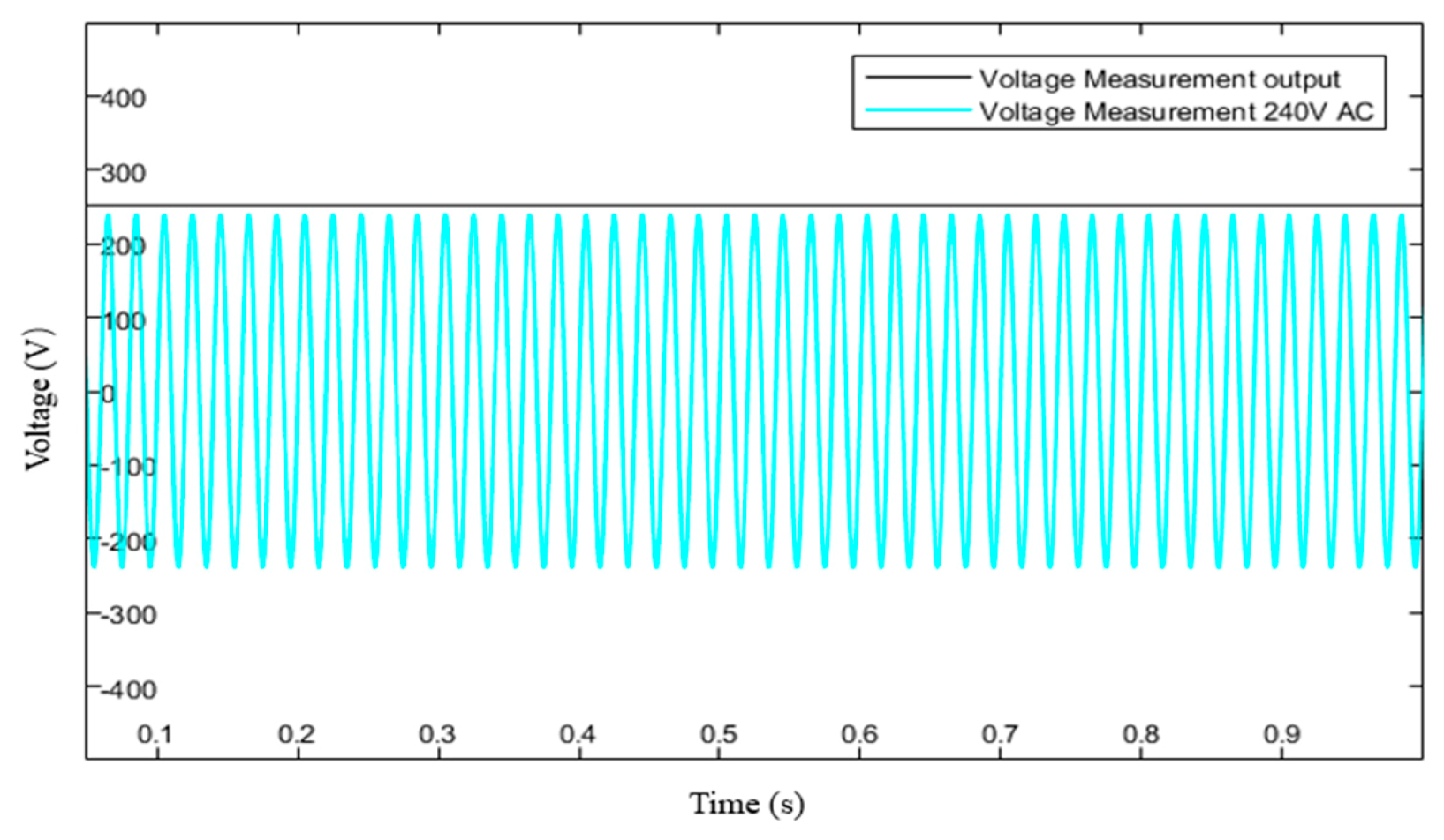
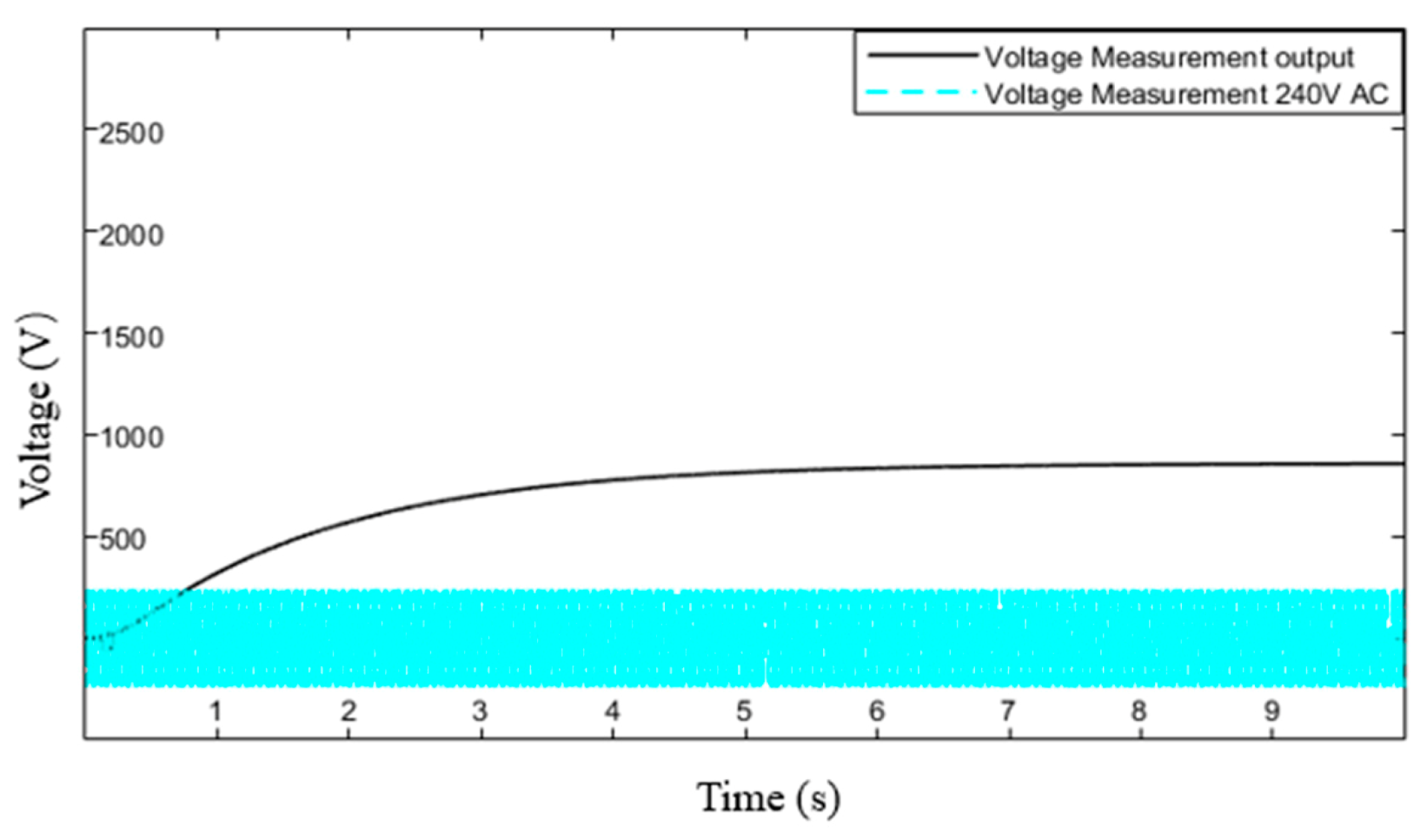
5.1. Output Current of Sample A
5.2. Influence on the Circuit of Sample B If IC Is Damaged
6. Conclusions and Outlook
Author Contributions
Funding
Data Availability Statement
Conflicts of Interest
References
- Khan, N.; Abas, N. Comparative study of energy saving light sources. Renew. Sustain. Energy Rev. 2011, 15, 296–309. [Google Scholar] [CrossRef]
- Mills, B.; Schleich, J. Household transitions to energy efficient lighting. Energy Econ. 2014, 46, 151–160. [Google Scholar] [CrossRef]
- Round, H.J. A Note on Carborundum. In Semiconductor Devices: Pioneering Papers; Sze, S.M., Ed.; World Scientific: Singapore, 1991. [Google Scholar]
- Holonyak, N.; Bevacqua, S.F. Coherent (visible) light emission from Ga(As1-xPx) junctions. Appl. Phys. Lett. 1962, 1, 82–83. [Google Scholar] [CrossRef]
- Nakamura, S.; Mukai, T.; Senoh, M. Candela-class high-brightness InGaN/AlGaN double-heterostructure blue-light emitting diodes. Appl. Phys. Lett. 1994, 64, 1687–1689. [Google Scholar] [CrossRef]
- Nishiura, S.; Tanabe, S.; Fujioka, K.; Fujimoto, Y. Properties of transparent Ce:YAG ceramic phosphors for white LED. Opt. Mater. 2011, 33, 688–691. [Google Scholar] [CrossRef]
- Zhang, C.; Heeger, A.J. Gallium nitride conjugated polymer hybrid light emitting diodes: Performance and lifetime. J. Appl. Phys. 1998, 83, 1579–1582. [Google Scholar] [CrossRef]
- Sun, B.; Fan, X.J.; Ye, H.Y.; Fan, J.J.; Qian, C.; van Driel, W.; Zhang, G.Q. A novel lifetime prediction for integrated LED lamps by electronic-thermal simulation. Reliab. Eng. Syst. Saf. 2017, 163, 14–21. [Google Scholar] [CrossRef]
- Humphreys, C.J. Solid-state lighting. MRS Bull. 2008, 33, 459–470. [Google Scholar] [CrossRef]
- Lafont, U.; van Zeijl, H.; van der Zwaag, S. Increasing the reliability of solid state lighting systems via self-healing approaches: A review. Microelectron. Reliab. 2012, 52, 71–89. [Google Scholar] [CrossRef]
- Perpina, X.; Werkhoven, R.; Jakovenko, J.; Formanek, J.; Vellvehi, M.; Jorda, X.; Kunen, J.; Bancken, P.; Bolt, P.J. Design for reliability of solid state lighting systems. Microelectron. Reliab. 2012, 52, 2294–2300. [Google Scholar] [CrossRef]
- Bergh, A.A.; Dean, P.J. Light-emitting diodes. Proc. IEEE 1972, 60, 156–223. [Google Scholar] [CrossRef]
- Bakin, N.N.; Tuyev, V.I.; Yauk, E.F. LED lighting. In Proceedings of the 12th International Conference Seminar of Young Specialists on Micro/Nanotechnologies and Electron Devices (EDM), Erlagol, Altai, Russia, 30 June–4 July 2011; pp. 346–348. [Google Scholar]
- Lall, P.; Sakalaukus, P.; Davis, L. Reliability and failure modes of solid-state lighting electrical drivers subjected to accelerated aging. IEEE Access 2015, 3, 531–542. [Google Scholar] [CrossRef]
- Lall, P.; Zhang, H.; Davis, L. Failure mechanisms and color stability in light-emitting diodes during operation in high-temperature environments in presence of contamination. In Proceedings of the IEEE 65th Electronic Components and Technology Conf. (ECTC), San Diego, CA, USA, 26–29 May 2015; pp. 1624–1632. [Google Scholar]
- Wang, X.X.; Jing, L.; Wang, Y.; Gao, Q.; Sun, Q. The influence of junction temperature variation of LED on the lifetime estimation during accelerated aging test. IEEE Access 2019, 7, 4773–4781. [Google Scholar] [CrossRef]
- Lall, P.; Wei, J.; Davis, L. Solid state lighting life prediction using extended Kalman filter. In Proceedings of the ASME 2013 International Technical Conference and Exhibition on Packaging and Integration of Electronic and Photonic Microsystems-InterPACK2013, Burlingame, CA, USA, 16–18 July 2013; article iPACK2013-73288. pp. 1–11. [Google Scholar]
- Chen, Q.; Chen, Q.; Luo, X.B. Fast estimation of LED’s accelerated lifetime by online test method. In Proceedings of the IEEE 64th Electronic Components and Technology Conference (ECTC), Lake Buena Vista, FL, USA, 27–30 May 2014; pp. 1992–1995. [Google Scholar]
- Qian, C.; Fan, J.J.; Fan, X.J.; Chernyakov, A.E.; Zhang, G.Q. Lumen and chromacity maintenance lifetime prediction for LED lamps using a spectral power distribution method. In Proceedings of the 12th International Forum on Solid State Lighting (SSL China), Shenzhen, China, 2–4 November 2015; pp. 67–70. [Google Scholar]
- Pimputkar, S.; Speck, J.S.; Denbaars, S.P.; Nakamura, S. Prospects for LED lighting. Nat. Photonics 2009, 3, 179–181. [Google Scholar] [CrossRef]
- Lee, Y.-S.; Chow, M.H.L. Diode rectifiers. In Power Electronics Handbook, 3rd ed.; Rashid, M.H., Ed.; Butterworth-Heinemann: Burlington, MA, USA, 2011; Chapter X; pp. 149–182. [Google Scholar]
- Storr, W. Full Wave Rectifier. Available online: https://www.electronics-tutorials.ws/diode/diode_6.html (accessed on 24 May 2021).
- Williams, A.B.; Taylor, F.J. Electronic Filter Design Handbook, 4th ed.; McGraw-Hill: New York, NY, USA, 2006. [Google Scholar]
- Non-Isolated Buck Offline LED Driver, Bright Power Semiconductor Co., Data Sheet BP2832A, Rev.1.0. Available online: http://www.datasheet.es/PDF/864023/BP2832A-pdf.html (accessed on 27 May 2021).
- Freitas, P.; Navarro, D.; O’Connor, I.; Billiot, G.; Lapuyade, H.; Begueret, J.B. Analog circuit design. In Planar Double-Gate Transistor: From Technology to Circuit; Amara, A., Rozeau, O., Eds.; Springer: Berlin, Germany, 2009; Chapter 5; pp. 105–136. [Google Scholar]
- Van Driel, W.; Evertz, F.; Zhang, G.Q. Towards a system level reliability approach for solid state lighting. J. Light Vis. Env. 2011, 35, 267–273. [Google Scholar] [CrossRef][Green Version]
- de Santi, C.; dal Lago, M.; Buffolo, M.; Monti, D.; Meneghini, M.; Meneghesso, G.; Zanoni, E. Failure causes and mechanisms of retrofit LED lamps. Microelectron. Reliab. 2015, 55, 1765–1769. [Google Scholar] [CrossRef]
- Hui, S.Y.; Li, S.N.; Tao, X.H.; Chen, W.; Ng, W.M. A novel passive offline LED driver with long lifetime. IEEE Trans. Power Electron. 2010, 25, 2665–2672. [Google Scholar] [CrossRef]


| Criterion | Sample A | Sample B |
|---|---|---|
| Manufacturer | unknown | Diall |
| Failure type | no light output | flickering |
| Input voltage | 220–240 V AC | 220–240 V AC |
| Rated working current | 35 mA | 44 mA |
| Power consumption | 4 W | 4.5 W |
| Nominal brightness | 230 lm | 230 lm |
| Frequency | 50 Hz | 50 Hz |
| Part Name | Function |
|---|---|
| Optics | Guide light from LED head to yield even illumination |
| LED head | Light-emitting part of the device, usually composed of multiple sets of single LEDs |
| Heat sink | Dissipates heat from LED head and drive circuits |
| Drive circuit | Converts 220–240 V AC to several volts DC, at 10s of milliamps of constant current DC to drive LEDs |
| Socket base | Provides electrical contact to lamp holder |
| Parameter | Value |
|---|---|
| Turn-on voltage of VCC | 13.8 V |
| Clamp voltage of VCC | 16.8 V |
| Input voltage range of circuit | 176 to 265 V |
| Minimum LED loading voltage | 15 V |
| Internal reference voltage for CS | 400 mV |
| Component | Nominal Value | Measured Value |
|---|---|---|
| R1 | 5.1 kΩ | 5.3 MΩ |
| R2 | 470 kΩ | 430.5 kΩ |
| R3 | 470 kΩ | 471.2 kΩ |
| R4 | 470 kΩ | 461.6 kΩ |
| R5 | 100 kΩ | 99.5 kΩ |
| R6 | 2 Ω | 2.1 Ω |
| R7 | 2 Ω | 2 Ω |
| R8 | 470 kΩ | 451.1 kΩ |
| R9 | 1 MΩ | 1.1 MΩ |
| C1 | 0.1 μF | 0.1 μF |
| C2 | 2.2 μF | 2.1 μF |
| C3 | 2.2 μF | 1.79 μF |
| C4 | 0.1 μF | 0.1 μF |
| C5 | 0.1 μF | 0.1 μF |
| L1 | 2.2 μH | open |
| L2 | 2 mH | 2 mH |
| BD1, D1, F1 | normal | |
| Component | Nominal Value | Measured Value |
|---|---|---|
| R1 | 5.1 kΩ | 5.1 kΩ |
| R2 | 240 kΩ | 240.4 kΩ |
| R3 | 240 kΩ | 239.2 kΩ |
| R4 | 1 kΩ | 1 kΩ |
| R5 | 2 Ω | 2.07 Ω |
| R6 | 2 Ω | 2.1 Ω |
| R7 | 330 kΩ | 327.5 kΩ |
| CX1 | 0.1 μF | 0.1 μF |
| C1 | 2.2 μF | 2.04 μF |
| C2 | 2.2 μF | 2.06 μF |
| C3 | 0.1 μF | 0.1 μF |
| C4 | 2.2 μF | 2.69 μF |
| C5 | 0.1 μF | Open |
| L1 | 4.7 μH | 4.72 μH |
| L2 | 1.25 mH | 1.24 mH |
| BD1, D1, F1 | normal | |
Publisher’s Note: MDPI stays neutral with regard to jurisdictional claims in published maps and institutional affiliations. |
© 2021 by the authors. Licensee MDPI, Basel, Switzerland. This article is an open access article distributed under the terms and conditions of the Creative Commons Attribution (CC BY) license (https://creativecommons.org/licenses/by/4.0/).
Share and Cite
Zhong, W.; Walther, T. Failure Analysis of Some Commercial Spotlights Based on Light Emitting Diodes. Electronics 2022, 11, 48. https://doi.org/10.3390/electronics11010048
Zhong W, Walther T. Failure Analysis of Some Commercial Spotlights Based on Light Emitting Diodes. Electronics. 2022; 11(1):48. https://doi.org/10.3390/electronics11010048
Chicago/Turabian StyleZhong, Wei, and Thomas Walther. 2022. "Failure Analysis of Some Commercial Spotlights Based on Light Emitting Diodes" Electronics 11, no. 1: 48. https://doi.org/10.3390/electronics11010048
APA StyleZhong, W., & Walther, T. (2022). Failure Analysis of Some Commercial Spotlights Based on Light Emitting Diodes. Electronics, 11(1), 48. https://doi.org/10.3390/electronics11010048