
A Referenceless Digital CDR with a Half-Rate Jitter-Tolerant FD and a Multi-Bit Decimator


Abstract
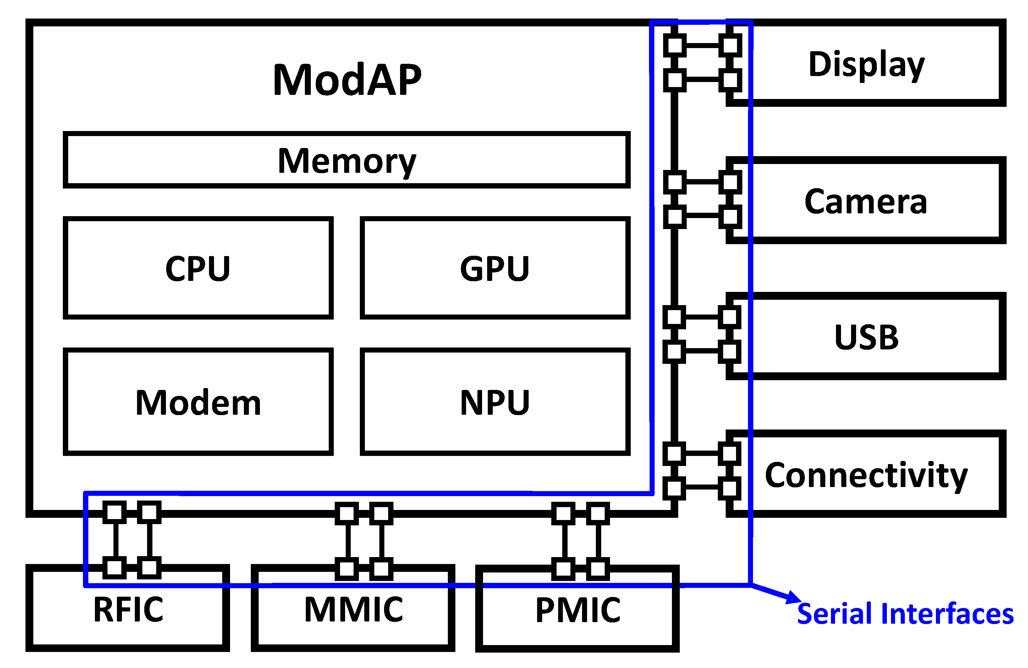
:1. Introduction
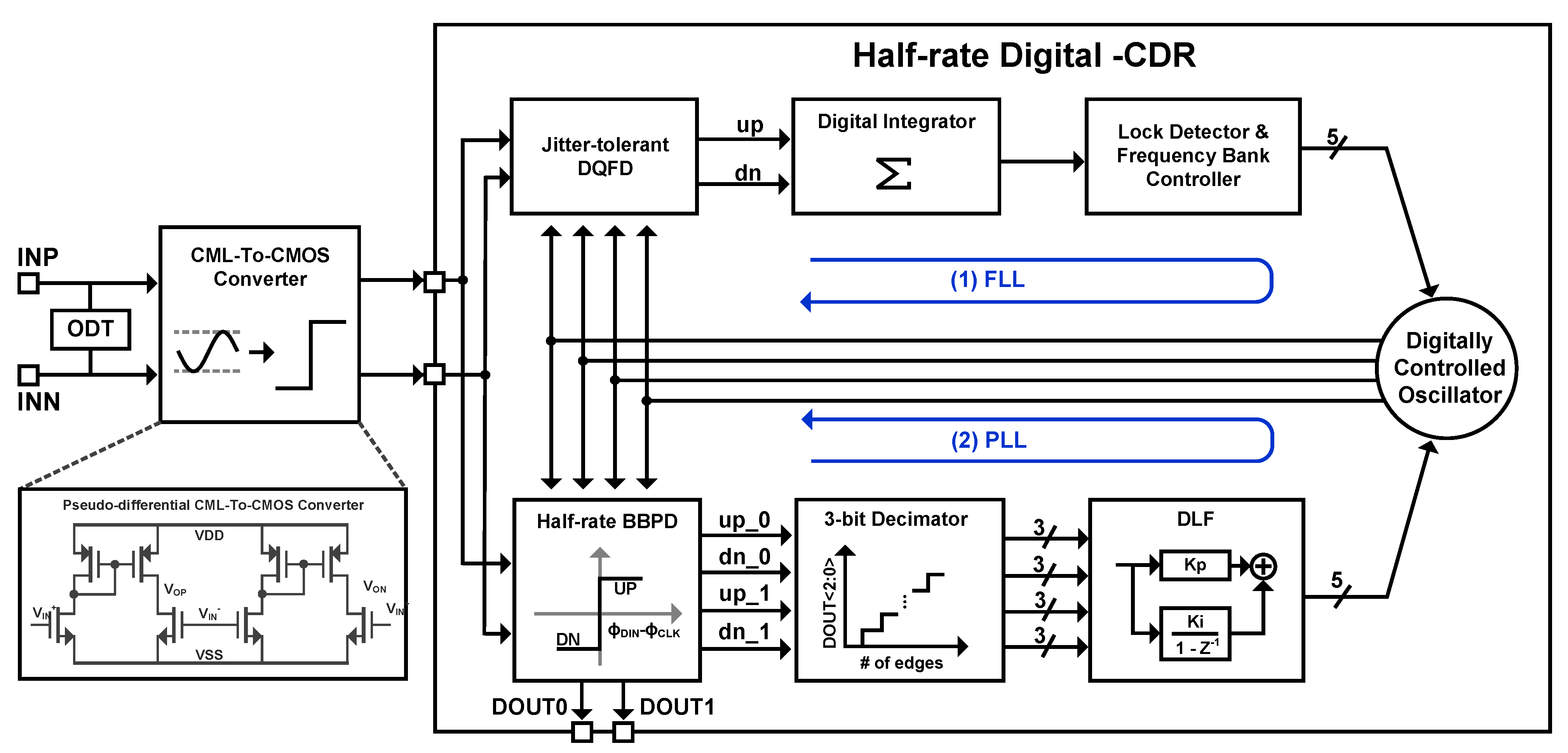
2. Digital CDR Architecture
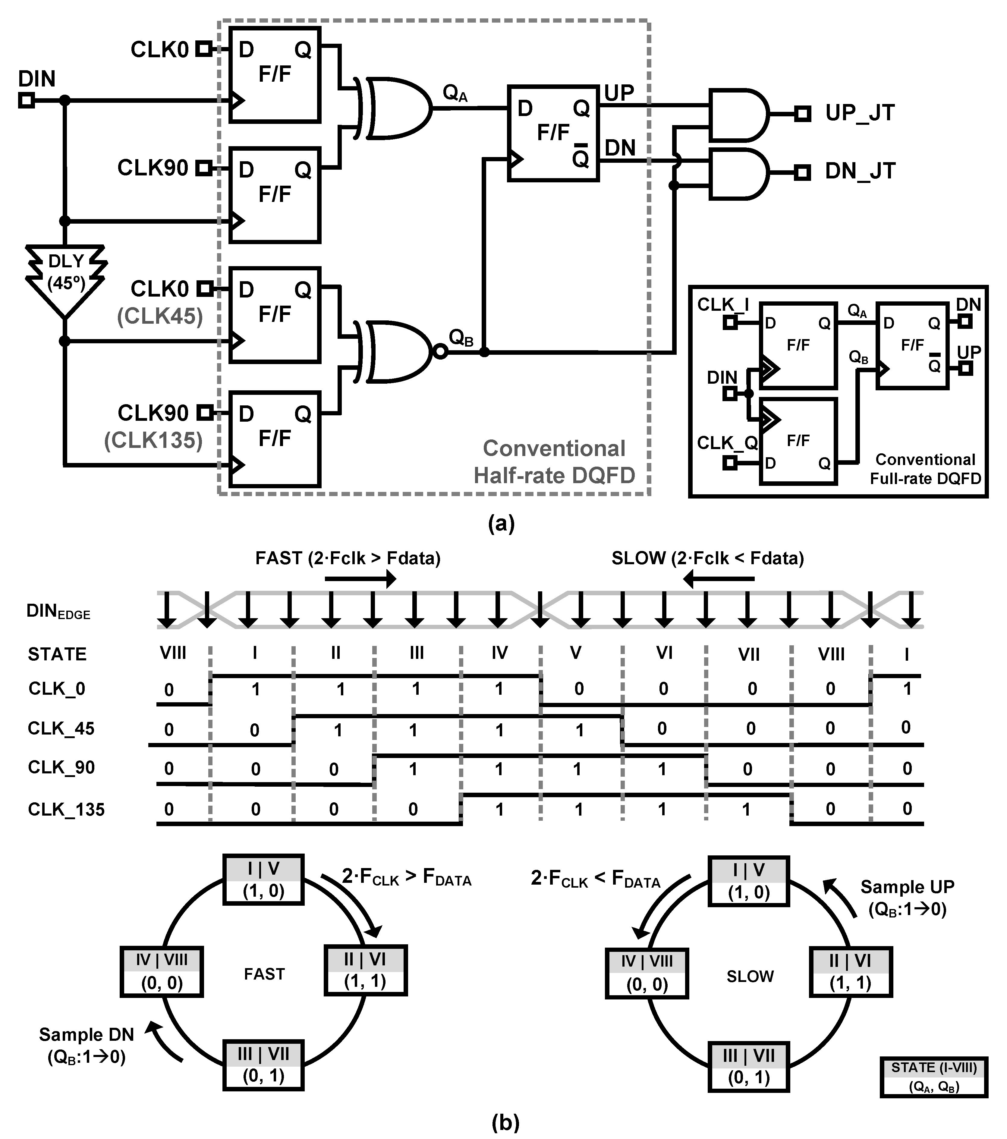
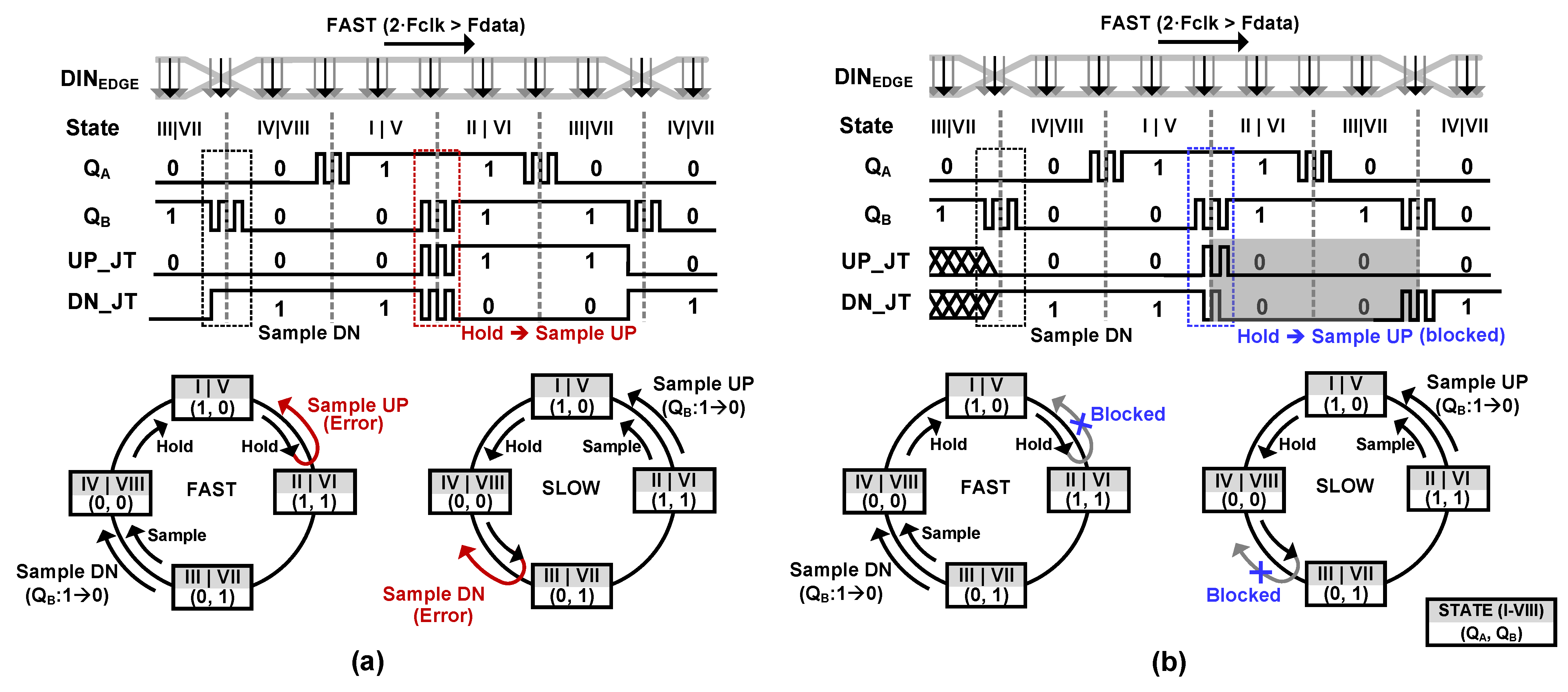
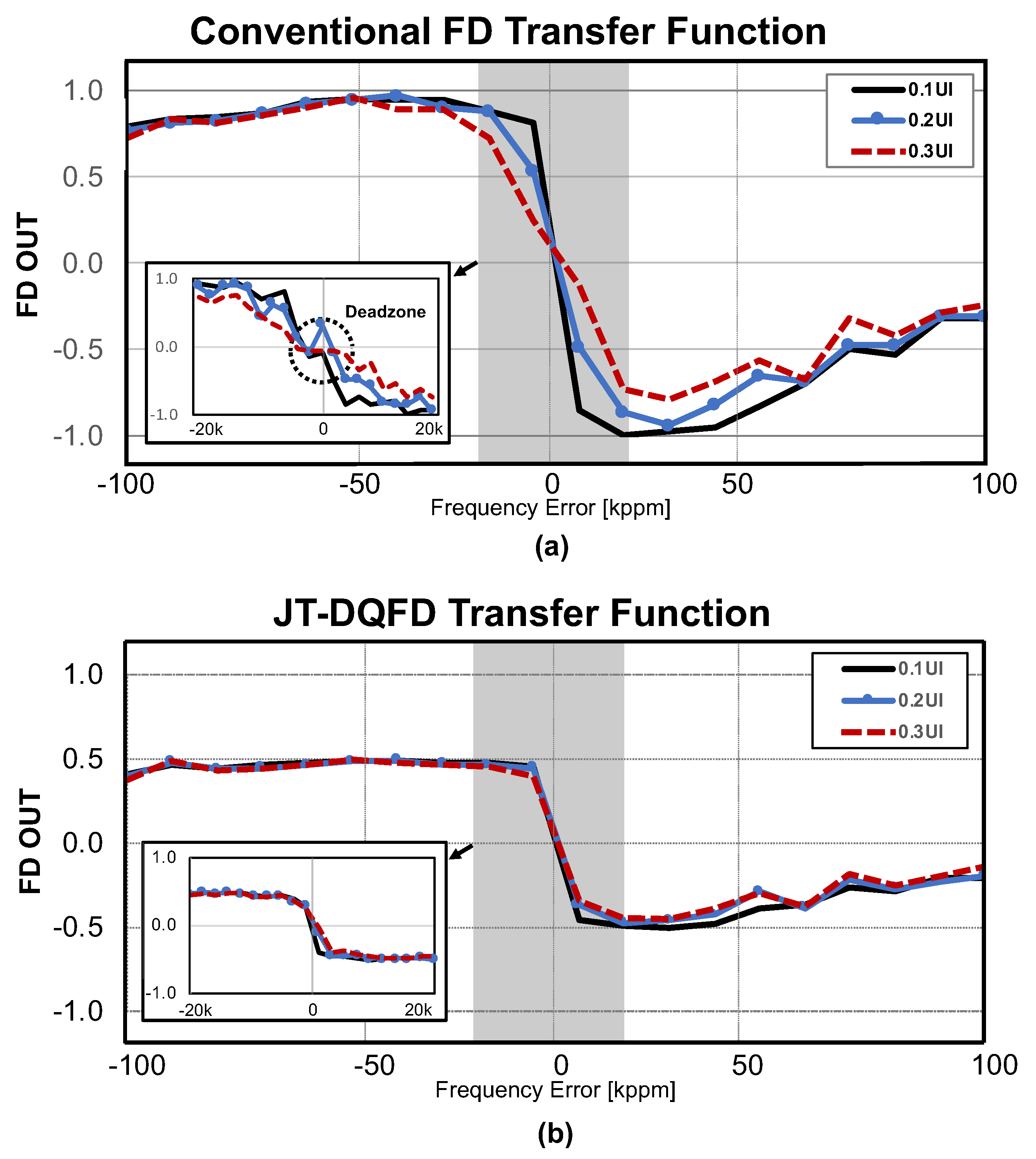
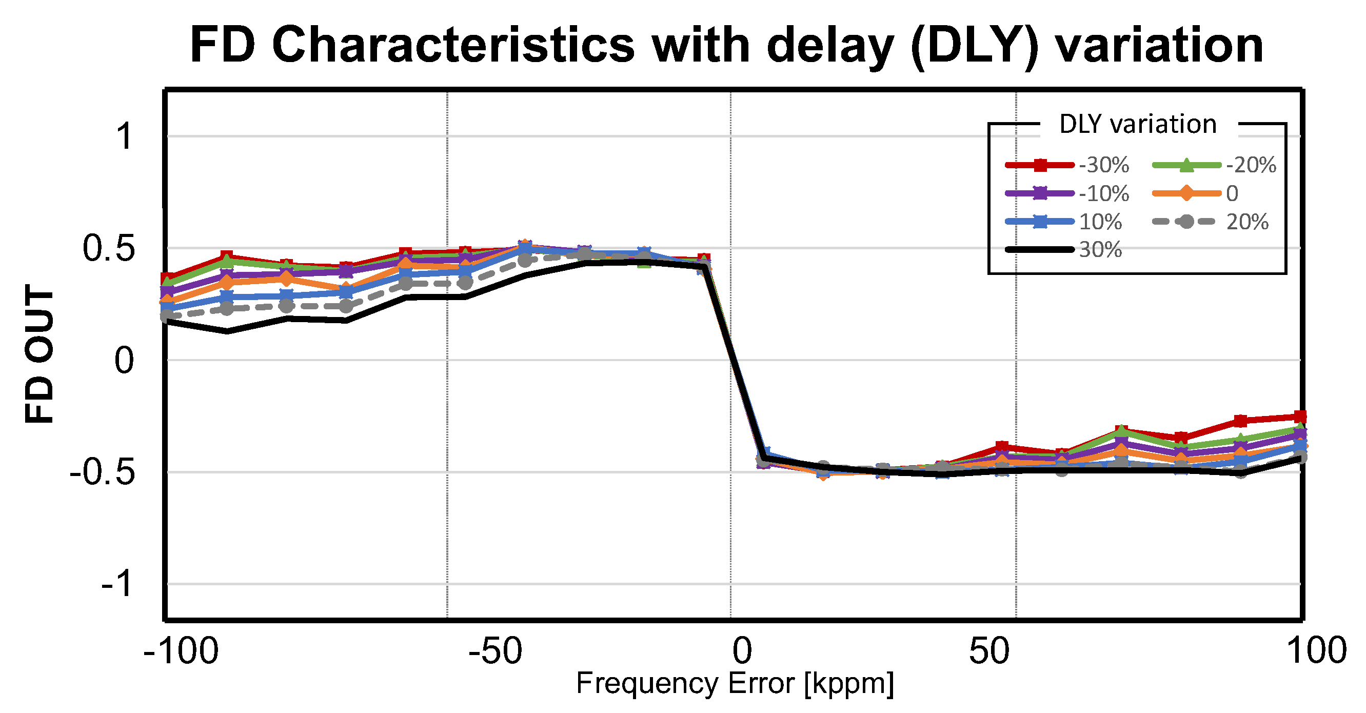
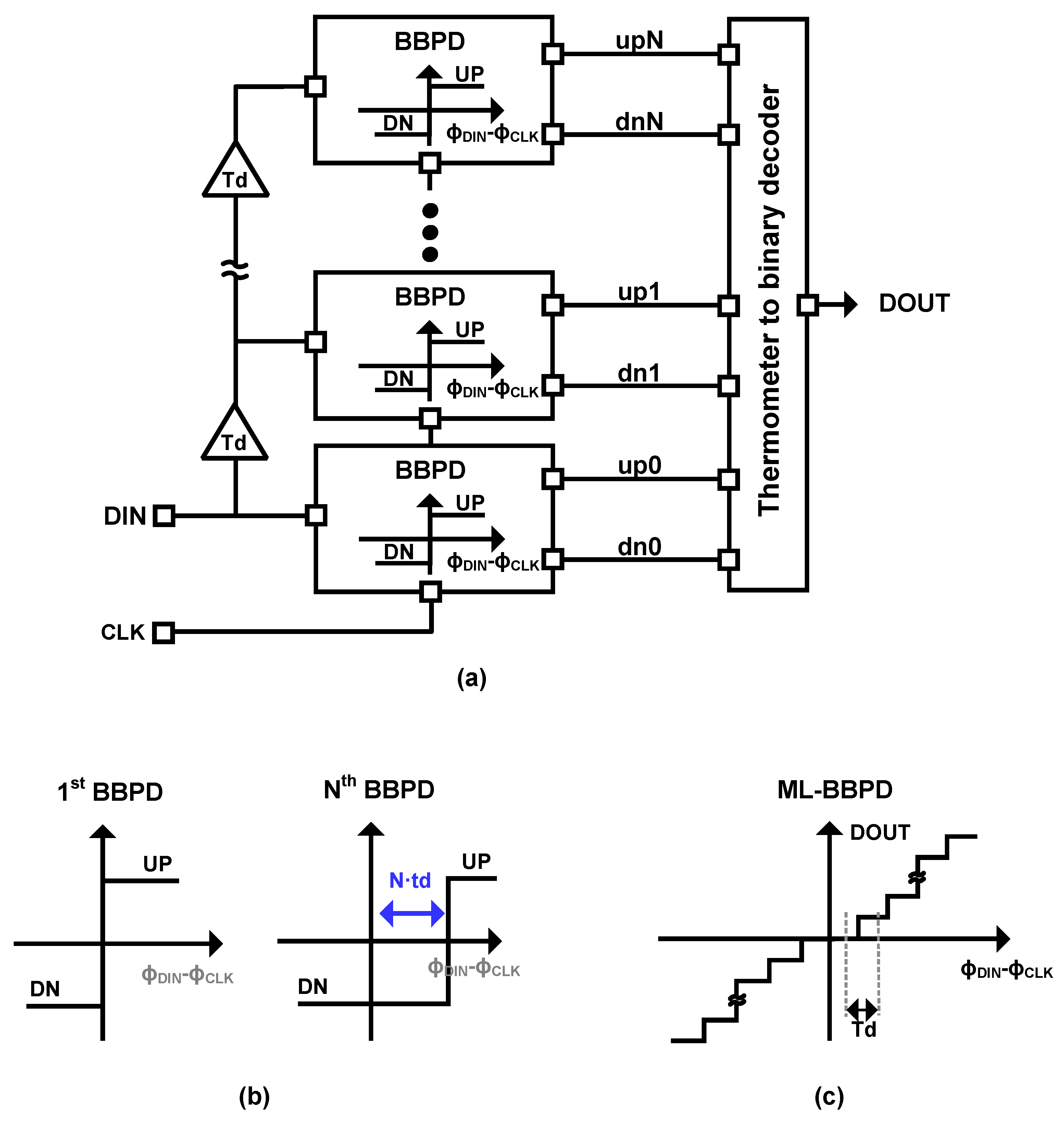
2.1. Jitter-Tolerant Frequency Detector
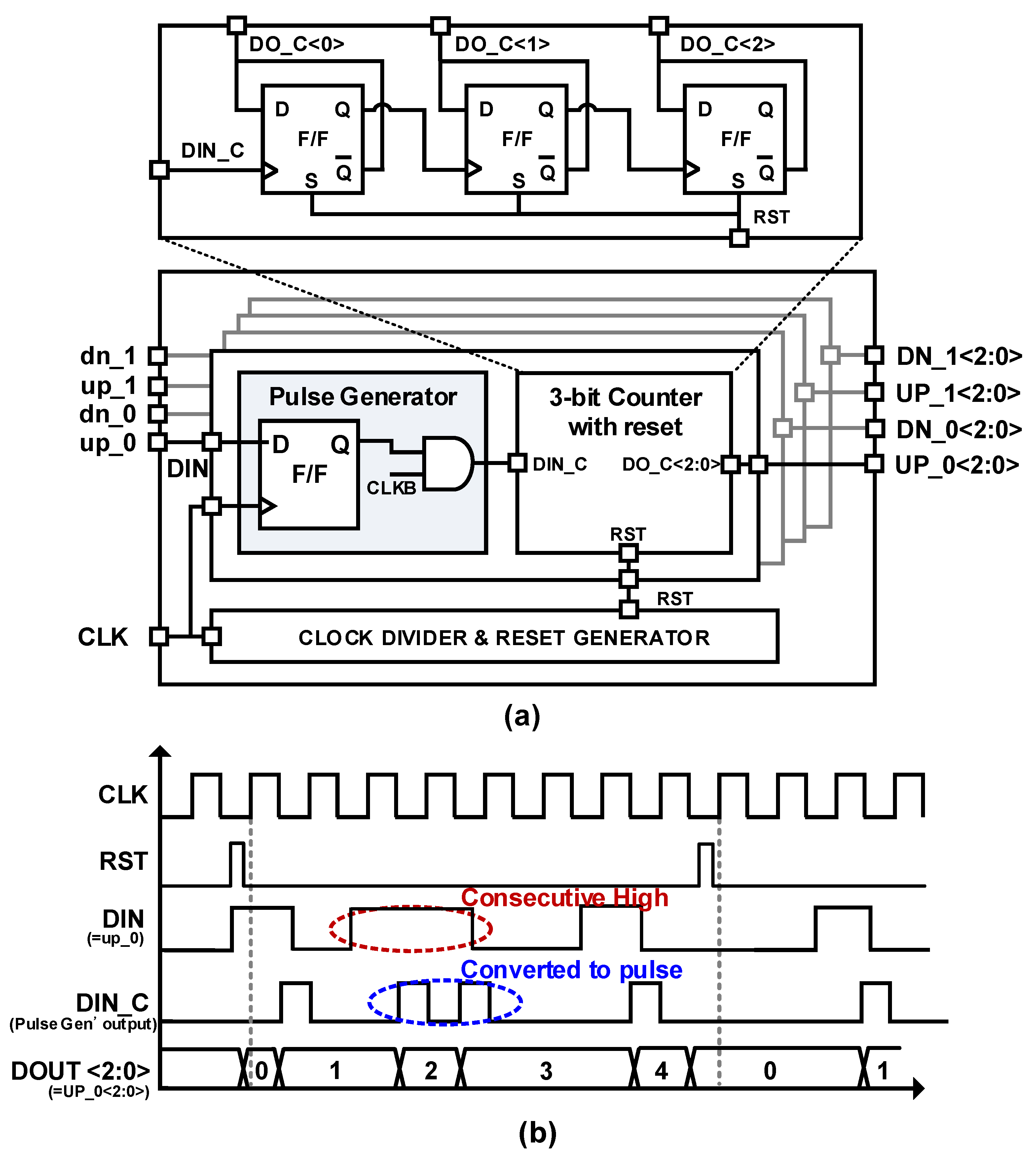
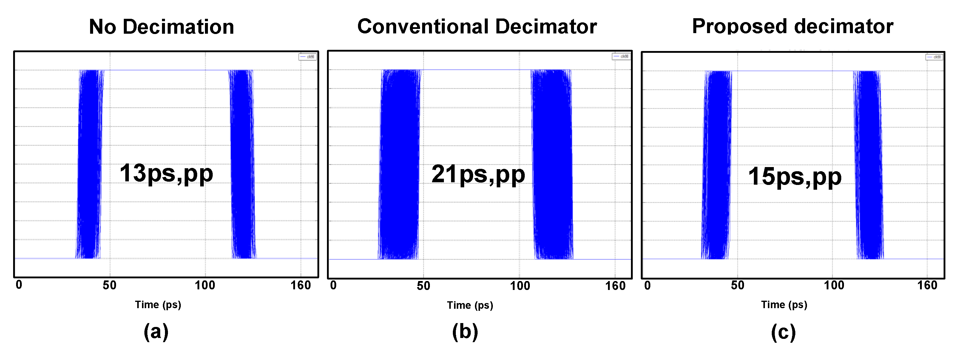
2.2. Multi-Bit Decimator with a Bangbang Phase Detector
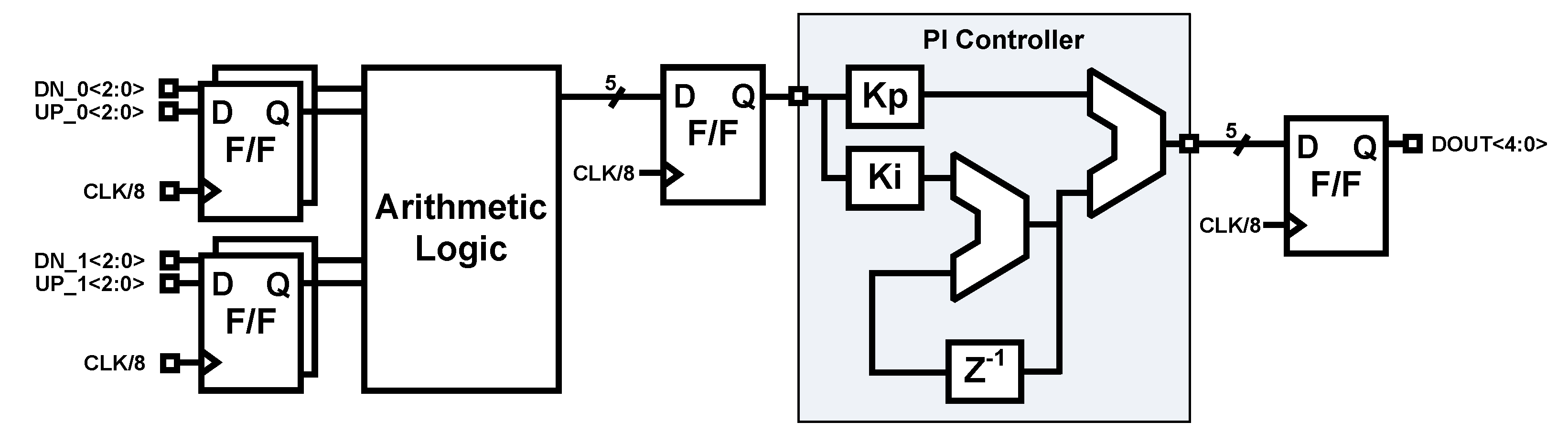
2.3. PI-Control Digital Loop Filter
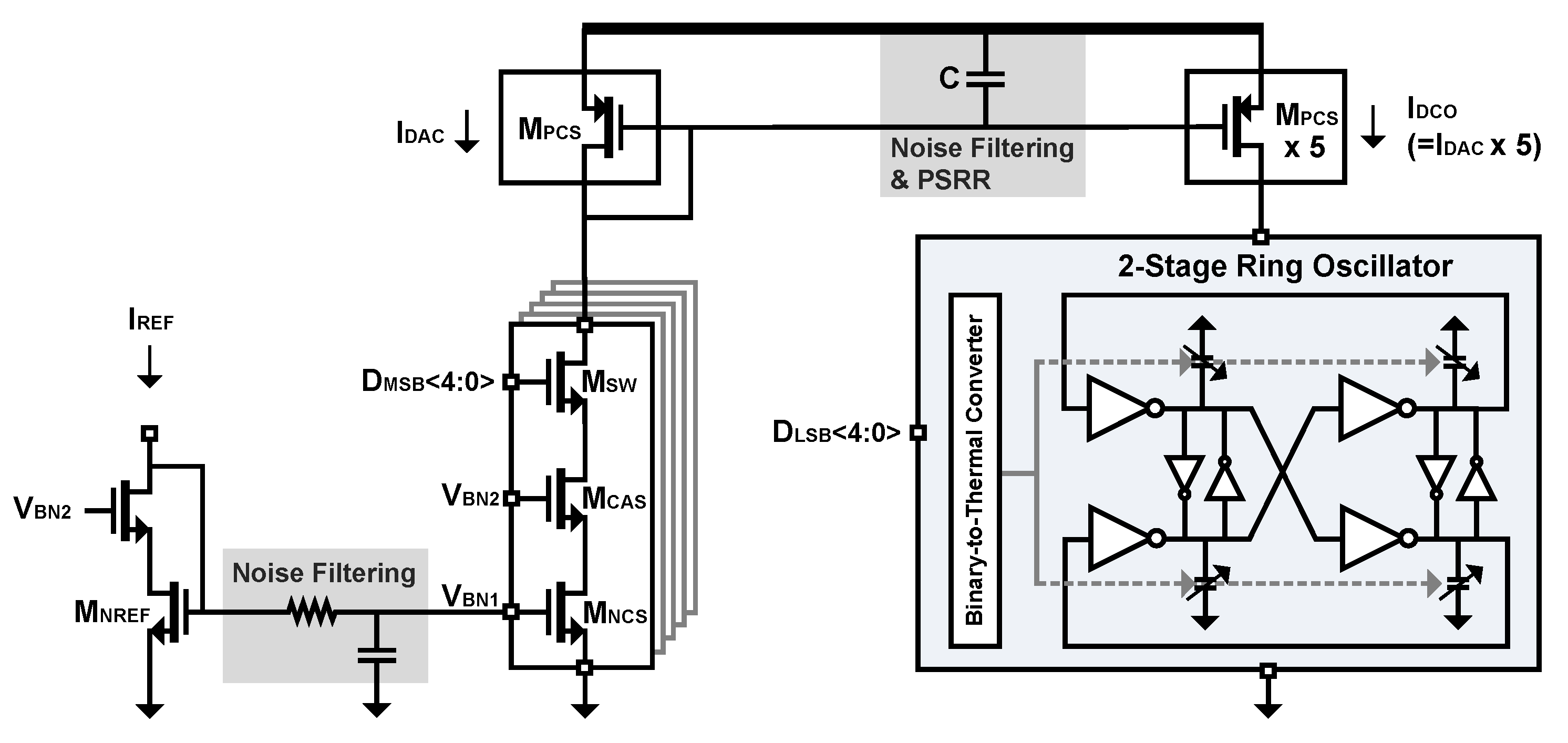
2.4. Digitally Controlled Oscillator
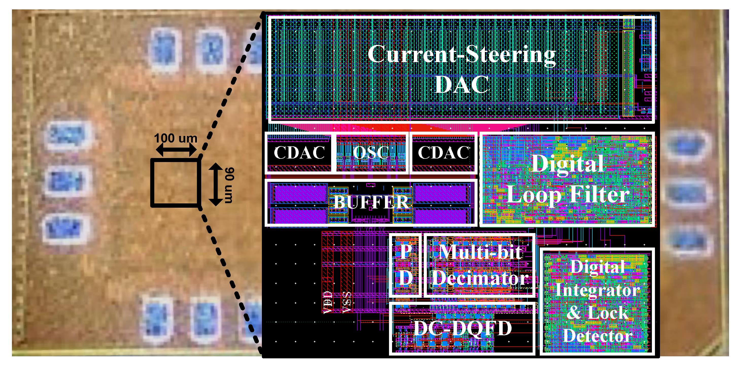
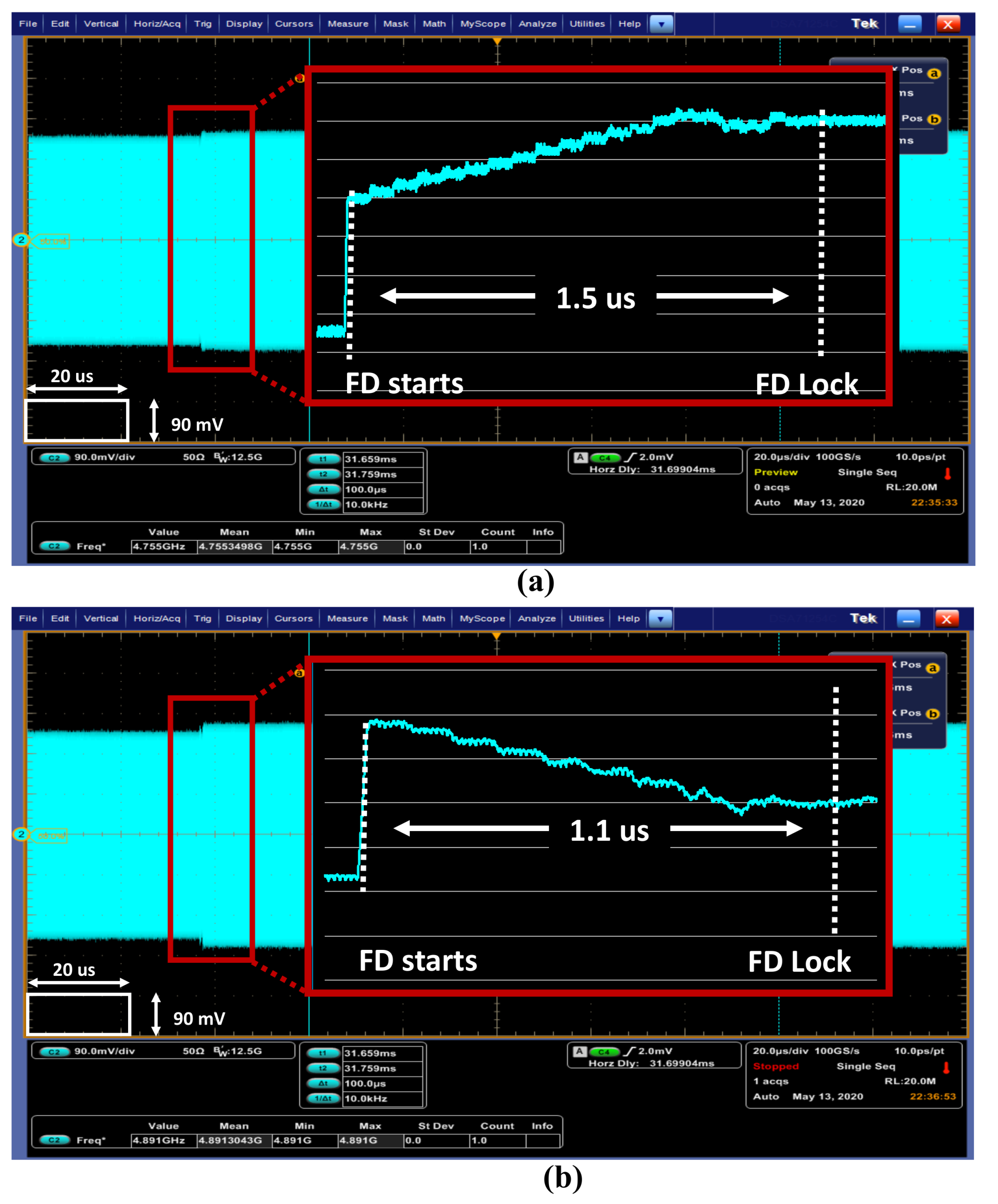
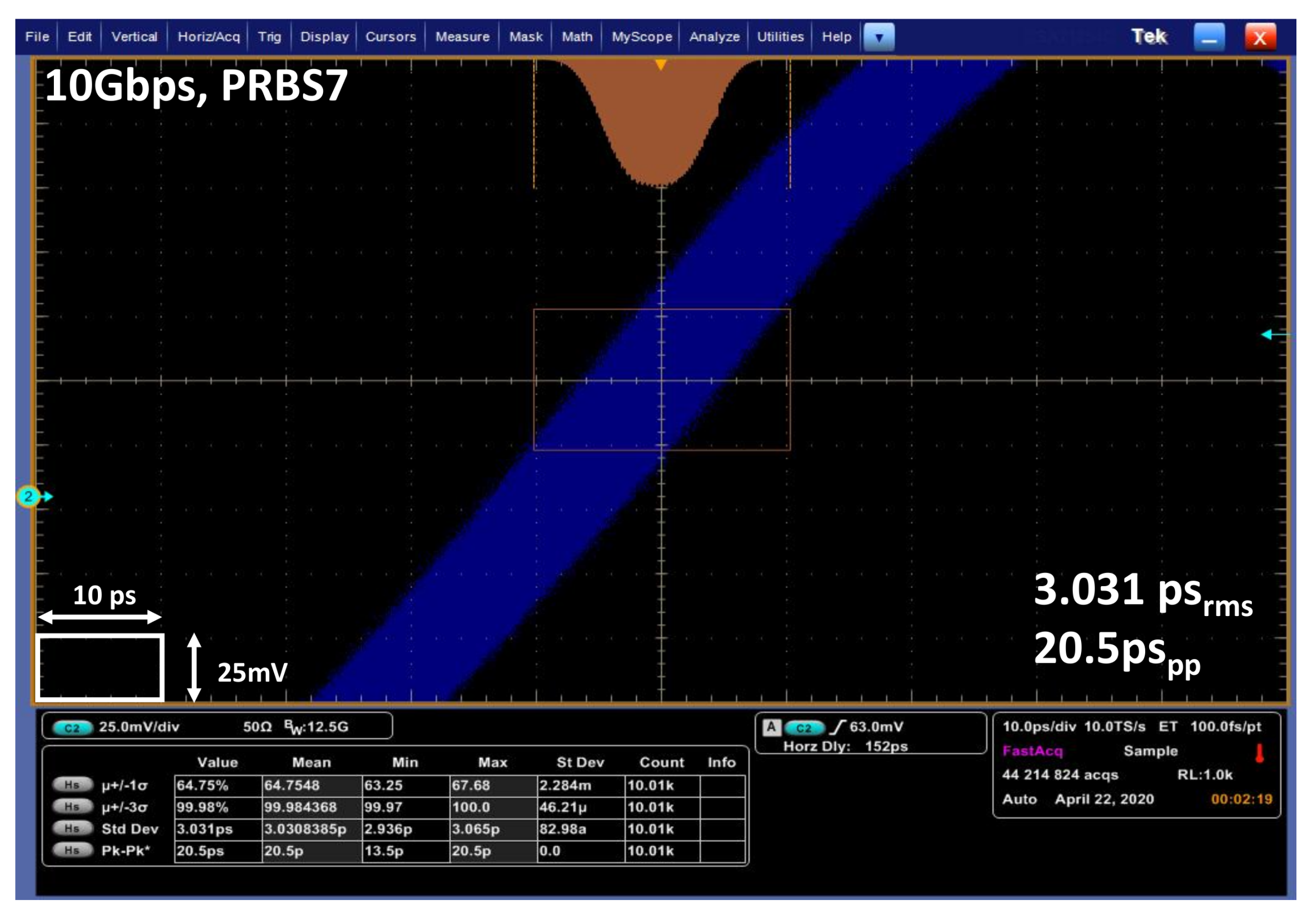
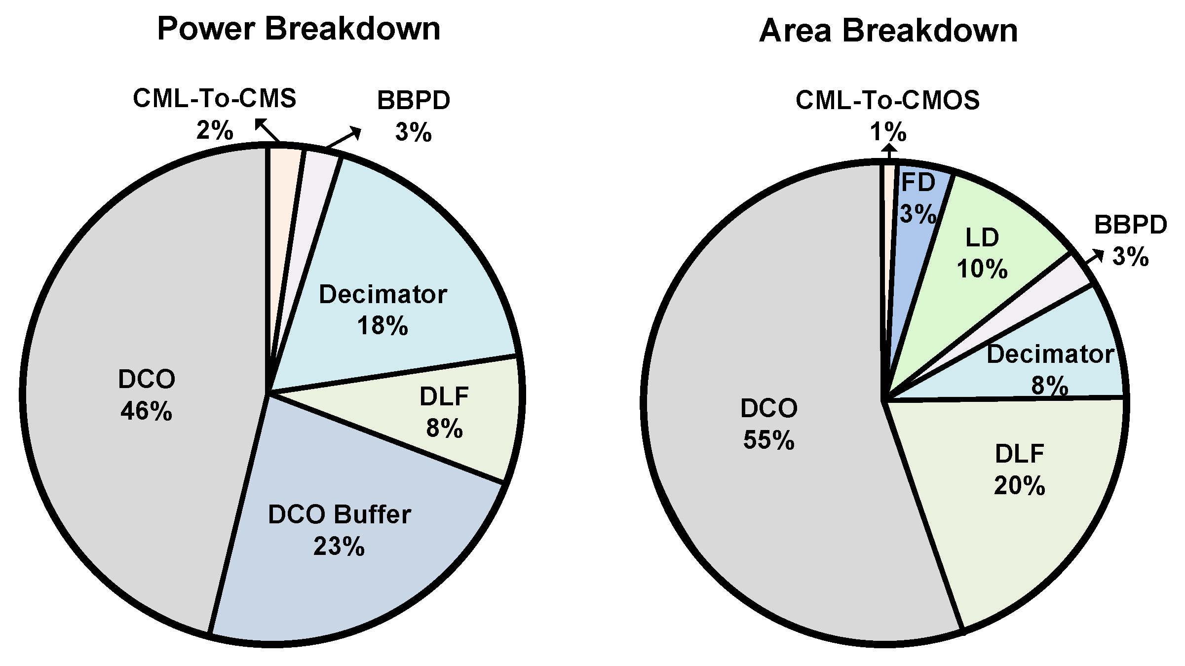
3. Measurement Results
4. Conclusions
Author Contributions
Funding
Conflicts of Interest
References
- Sonntag, J.L.; Stonick, J. A Digital Clock and Data Recovery Architecture for Multi-Gigabit/s Binary Links. IEEE J. Solid-State Circuit 2006, 41, 1867–1875. [Google Scholar] [CrossRef]
- Song, H.; Kim, D.-S.; Oh, D.-H.; Kim, S.; Jeong, D.-K. A 1.0-4.0-Gb/s All-Digital CDR with 1.0-ps Period Resolution DCO and Adaptive Proportional Gain Control. IEEE J. Solid-State Circuit 2015, 46, 424–434. [Google Scholar] [CrossRef]
- Shu, G.; Choi, W.; Saxena, S.; Talegaonkar, M.; Anand, T.; Elkholy, A.; Elshazly, A.; Hanumolu, P.K. A 4-to-105 Gb/s Continuous Rate Digital Clock and Data Recovery with Automatic Frequency Acquisition. IEEE J. Solid-State Circuit 2016, 51, 428–439. [Google Scholar]
- Lee, K.; Sim, J.-Y. A 0.8-to-6.35 Gb/s Continuous-Rate Reference-Less Digital CDR with Half-Rate Common-Mode Clock-Embedded Signlaing. IEEE Trans. Circuits Syst. I 2016, 63, 482–493. [Google Scholar] [CrossRef]
- Kim, Y.; Lee, T.; Jeon, H.-K.; Lee, D.; Kim, L.-K. An Input Data and Power Noise Inducing Clock Jitter Tolerant Reference-Less Digital CDR for LCD Intra-Panel Interface. IEEE Trans. Circuits Syst. I 2017, 64, 823–835. [Google Scholar] [CrossRef]
- Park, K.; Lee, K.; Cho, S.Y.; Lee, J.; Hwang, J.; Choo, M.S.; Jeong, D.K. A 4-to-20 Gb/s 1.87 pJ/b Referenceless Digital CDR with Unlimited Frequency Detection Capability in 65 nm CMOS. In Proceedings of the IEEE Symposium on VLSI Circuits Digest of Technical Papers, Kyoto, Japan, 9–14 June 2019; pp. C194–C195. [Google Scholar]
- Kim, D.; Choi, W.-S.; Elkholy, A.; Kenney, J.; Hanumolu, P.K. A 15 Gb/s 1.9 pJ/bit sub-baud-rate digital CDR. In Proceedings of the IEEE Custom Integrated Circuits Conference, San Diego, CA, USA, 8–11 April 2018; pp. 1–4. [Google Scholar]
- Choi, S.; Son, H.; Shin, J.; Lee, S.-H.; Kim, B.; Park, H.-J.; Sim, J.-Y. A 0.65-to-10.5 Gb/s Referenceless CDR with Asynchronous Baud-Rate Sampling for Frequency Acquisition and Adaptive Equalization. IEEE Trans. Circuits Syst. I 2016, 63, 276–287. [Google Scholar] [CrossRef]
- Yang, R.-J.; Chen, S.-P.; Liu, S.-I. A 3.125-Gb/s clock and data recovery circuit for the 10-Gbase-LX4 Ethernet. IEEE J. Solid-State Circuit 2004, 39, 1356–1360. [Google Scholar] [CrossRef]
- Lee, Y.-L.; Chang, S.-J.; Chen, Y.-C.; Cheng, Y.-P. An unbounded frequency detection mechanism for continuous-rate CDR circuits. Trans. Circuits Syst. II Exp. Briefs 2017, 64, 500–504. [Google Scholar] [CrossRef]
- Jin, J.; Jin, X.; Jung, J.; Kwon, K.; Kim, J.; Chun, J.-H. A 0.75–3.0-Gb/s Dual-Mode Temperature-Tolerant Referenceless CDR with a Deadzone-Compensated Frequency Detector. IEEE J. Solid-State Circuit 2018, 53, 2994–3003. [Google Scholar] [CrossRef]
- Lee, J.; Kundert, K.S.; Razavi, B. Anaysis and Modeling of Bang-Bang Clock and Data Recovery Circuits. IEEE J. Solid-State Circuit 2004, 39, 1571–1580. [Google Scholar]
- Kwon, D.-H.; Park, Y.-S.; Choi, W.-Y. A Clock and Data Recovery Circuit with Programmable Multi-Level Phase Detector Characteristics and Bulit-in Jitter Monitor. IEEE Trans. Circuits Syst. I 2015, 62, 1472–1480. [Google Scholar] [CrossRef]
- Walker, R. Designing bang-bang PLLs for clock and data recovery in serial data transmission systems. In Phase-Locking in High-Performance Systems: From Device to Architectures; Razavi, B., Ed.; Wiley-IEEE Press: Hoboken, NJ, USA, 2003; pp. 34–35. [Google Scholar]
- Nonis, R.; Grollitsch, W.; Santa, T.; Cherniak, D.; da Dalt, N. A 2.4 psrms-jitter Digital PLL with Multi-Output Bang-Bang Phase Detectr andPhase-Interpolator-Based Fractional-N Divider. In Proceedings of the IEEE International Solid-state Circuits Conference–(ISSCC), San Francisco, CA, USA, 17–21 February 2013. [Google Scholar]
- Gimeno, C.; Bol, D.; Flandre, D. Multilevel Half-Rate Phase Detector for Clock and Data Recovery Circuits. IEEE Trans. Very Large Scale Integr. (VLSI) Syst. 2018, 26, 1807–1811. [Google Scholar] [CrossRef]
- Sánchez-Azqueta, C.; Gimeno, C.; Aldea, C.; Celma, S. New Multilevel Bang-Bang Phase Detector. IEEE Trans. Instrum. Meas. 2013, 62, 3384–3386. [Google Scholar] [CrossRef]
- Pelgrom, M.; Duinmaijer, A.; Welbers, A. Matching properties of MOS transistors IEEE J. Solid-State Circuits 1989, 24, 1433–1439. [Google Scholar] [CrossRef]
- Shen, K.J.; Farooq, S.F.S.; Fan, Y.; Nguyen, K.M.; Wang, Q.; Elshazly, A.; Kurd, N. A 0.17-to-3.5 mW 0.15-to-5 GHz SoC PLL with 15 dB built-in supply noise rejection and self-bandwidth control in 14 nm CMOS. In Proceedings of theIEEE International Solid-state Circuits Conference–(ISSCC), San Francisco, CA, USA, 31 January–4 Febuary 2016. [Google Scholar]
- Kim, J.; Ko, Y.; Jin, J.; Choi, J.; Chun, J.-H. A Jitter-Tolerant Referenceless Digital-CDR for Cellular Transceivers. In Proceedings of the IEEE Asian Solid-State Circuits Conference (A-SSCC), Hiroshima, Japan, 4–9 November 2020. [Google Scholar]


| JSSC 16’ [3] | TCAS-1 16’ [4] | TCAS-I 17’ [5] | VLSI 19’ [6] | This Work | |
|---|---|---|---|---|---|
| process [nm] | 65 | 65 | 65 | 65 | 28 |
| data rate [Gb/s] | 4–10.5 | 0.8–6.5 | 10 | 4–20 | 9.5–10.5 |
| supply [V] | 1.2/1.0 | 1.2 | 1.2 | 1.2 | 1.0 |
| clock rate | half-rate | half-rate | quarter-rate | half-rate | half-rate |
| data pattern | PRBS7 (JTOL) PRBS31(CLK) | PRBS31 | PRBS7 | PRBS31 | PRBS7 |
| clock jitter [ps/ps] | 2.2/24 | 4.04/38.2 | 2.45/32.3 | 1.95/12.8 | 3.03/20.5 |
| high frequency JTOL[UI] | 0.4 * | - | 0.22 | 0.42 | 0.25 |
| area [mm] | 1.63 | 0.018 | 0.117 | 0.045 | 0.009 |
| power [mW] | 22.5@10G | 15.6@6.5G | 20.7@10G ** | 37.3@20G | 13@10G *** |
| FoM [pJ/bit] | 2.25 | 2.4 | 2.07 ** | 1.87 | 1.3 *** |
Publisher’s Note: MDPI stays neutral with regard to jurisdictional claims in published maps and institutional affiliations. |
© 2022 by the authors. Licensee MDPI, Basel, Switzerland. This article is an open access article distributed under the terms and conditions of the Creative Commons Attribution (CC BY) license (https://creativecommons.org/licenses/by/4.0/).
Share and Cite
Kim, J.; Ko, Y.; Jin, J.; Choi, J.; Chun, J.-H. A Referenceless Digital CDR with a Half-Rate Jitter-Tolerant FD and a Multi-Bit Decimator. Electronics 2022, 11, 537. https://doi.org/10.3390/electronics11040537
Kim J, Ko Y, Jin J, Choi J, Chun J-H. A Referenceless Digital CDR with a Half-Rate Jitter-Tolerant FD and a Multi-Bit Decimator. Electronics. 2022; 11(4):537. https://doi.org/10.3390/electronics11040537
Chicago/Turabian StyleKim, Jaekwon, Youngjun Ko, Jahoon Jin, Jaehyuk Choi, and Jung-Hoon Chun. 2022. "A Referenceless Digital CDR with a Half-Rate Jitter-Tolerant FD and a Multi-Bit Decimator" Electronics 11, no. 4: 537. https://doi.org/10.3390/electronics11040537
APA StyleKim, J., Ko, Y., Jin, J., Choi, J., & Chun, J.-H. (2022). A Referenceless Digital CDR with a Half-Rate Jitter-Tolerant FD and a Multi-Bit Decimator. Electronics, 11(4), 537. https://doi.org/10.3390/electronics11040537