1. Introduction
Semiconductor quantum dots (QDs) are considered to significantly improve the efficiency of optoelectronic and nanophotonic devices because they are spatially limited in all three dimensions, which leads to their strong quantum confinement [
1,
2,
3,
4]. InAs QD lasers exhibit a low threshold current density [
5,
6], high internal quantum efficiency [
7,
8] and high-temperature stability of threshold current and slope efficiency [
9,
10]. However, output power and modulation bandwidth of QD lasers are still smaller than those characteristics of quantum well lasers [
11]. Furthermore, the performance of promising QD-based quantum information devices strongly depends on the geometry and composition of QDs [
12].
Photoluminescence (PL) spectra are normally taken from overgrown QDs whose geometrical parameters differ from those of uncovered QDs observed on the surface. Therefore, it is very essential to study the processes of QD capping. Previous studies by transmission electron microscopy (TEM) and cross-sectional scanning tunneling microscopy (X-STM) methods demonstrated that intensive mass transfer and intermixing occurs during overgrowth of InAs QDs [
11,
13,
14,
15,
16]. It was shown that the deposition of only one monolayer (ML) of GaAs above the array of QDs leads to a significant change in their size and density and to a clear bimodal size distribution [
17]. Another study demonstrated an abrupt decrease in the average height of InAs QDs from 10 to 1.5 nm after their overgrowth by a 2-nanometer-thick GaAs layer [
14]. The active mass transfer observed in these experiments is caused by a necessity to minimize the system energy by strain relaxation.
A lot of techniques were used to preserve the configuration of initial QDs. For example, overgrowth of InAs QDs by a GaAs layer at a temperature of 300 °C made it possible to maintain a pyramidal shape of QDs with sharp heterointerfaces [
13]. However, such low-temperature capping may result in poor structural and optical quality of QDs. Various overgrowth temperature sequences were also used to estimate their influence on the QD characteristics. The results indicate that the overgrowth temperature must be at the same level as or below the QD growth temperature to avoid intermixing and flushing of the tops of QDs [
11,
16,
18]. It was also shown that capping at low growth rates leads to more intensive intermixing and QD height reduction than at high growth rates [
15]. This indicates that the material of QDs and capping layers tends to intermix and transform into a single continuous layer when not prevented by specific techniques. For the same reason, any growth interruption leads to unceasing dissolving of QDs in the matrix material [
13]. However, much less attention has been paid to the dependence of the QD PL spectra on the arsenic beam equivalent pressure during overgrowth, which is also expected to have an impact on the processes of QD dissolving.
In this paper, we studied the influence of the arsenic pressure (PAs) during overgrowth of InAs QDs by a low-temperature GaAs (LT-GaAs) layer with different thicknesses (H) on the PL spectra of these structures. We revealed that a high arsenic pressure makes it possible to achieve a single broad line in the PL spectrum corresponding to unimodal size distribution of QDs, whereas the spectrum has two separate lines (~1080 and ~1150 nm) at a low arsenic pressure for both capping layer thicknesses (5 and 10 nm). An additional longwave line (~1150 nm) is attributed to the contribution of largened QDs. Their formation can be inhibited by increasing the arsenic flux, which suppresses mass transfer and reduces the contribution of large QDs in the PL spectrum.
2. Materials and Methods
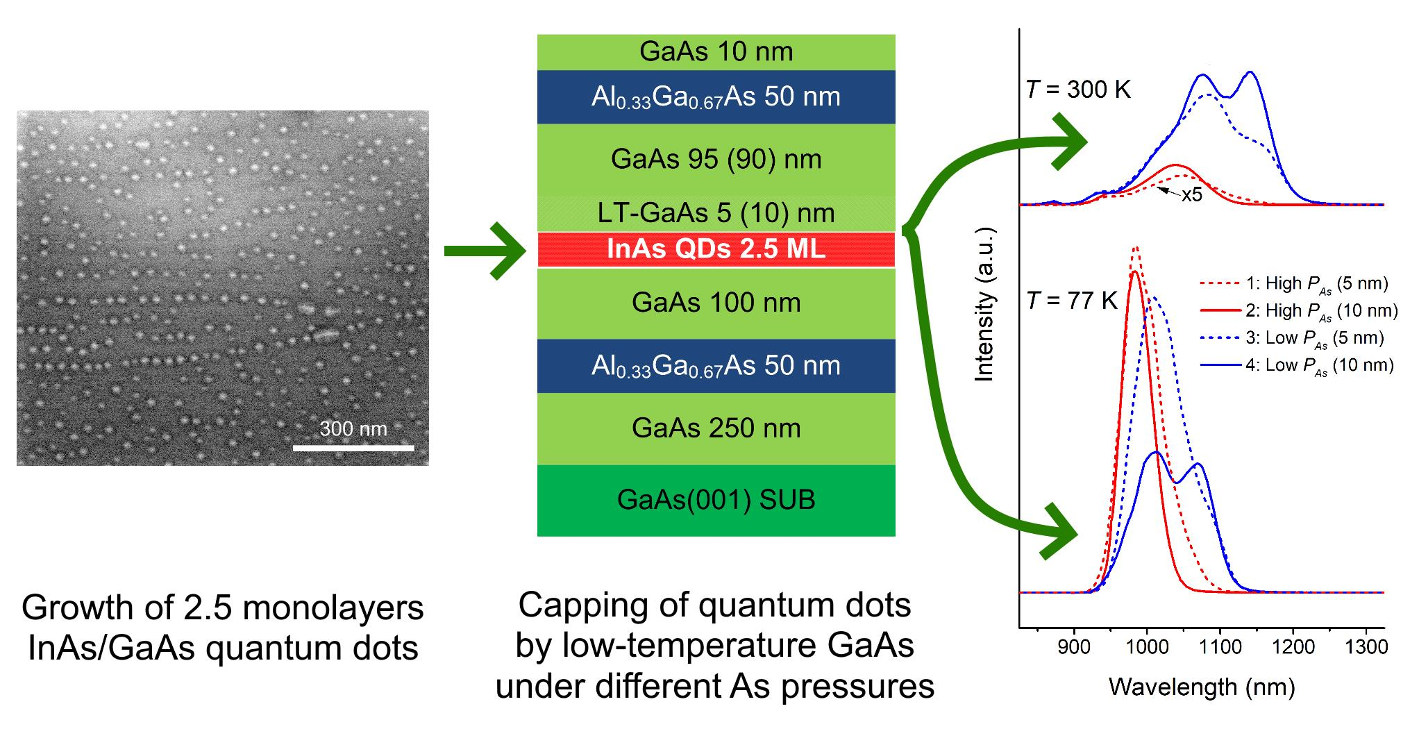
The samples were grown in a SemiTEq STE 35 solid-source molecular beam epitaxy system on GaAs(001) epi-ready substrates. Standard effusion cells were used as group-III component sources. For group-V arsenic, a valved cracker cell with As4 mode was used. After a standard procedure of the oxide removal, a 250-nanometer-thick GaAs buffer layer was grown at 580 °C. A single InAs QD layer was sandwiched between a 100-nanometer-thick GaAs inner layer and a 50-nanometer-thick Al0.33Ga0.67As outer layer grown at 580 °C and 600 °C, respectively. The QDs were formed by the Stranski–Krastanov growth mode after deposition of 2.5 MLs of InAs at 500 °C and 0.05 ML/s. The formation of InAs three-dimensional islands was verified by the streaky–spotty transition of the reflection high-energy electron diffraction pattern. After the QD formation, a growth interruption of 30 s under the arsenic flux was applied. Then, four different low-temperature (500 °C) GaAs capping procedures were carried out for samples 1–4: (1) 5 nm at PAs = 3 × 10⁻⁵ Pa; (2) 10 nm at PAs = 3 × 10⁻⁵ Pa; (3) 5 nm at PAs = 1 × 10⁻⁵ Pa; (4) 10 nm at PAs = 1 × 10⁻⁵ Pa. Thereafter, the substrate temperature was elevated to 580 °C to grow a high-temperature GaAs layer with a thickness of 95 nm for samples 1 and 3 and 90 nm for samples 2 and 4. Above the Al0.33Ga0.67As cladding layer, a 10-nanometer-thick high-temperature GaAs layer was grown, and the structure was annealed at 610 °C to reduce defects. For reference, an additional sample was grown with an array of uncovered QDs formed straightly on a GaAs buffer layer (sample 0).
A schematic QD PL structure grown in this study is illustrated in
Figure 1.
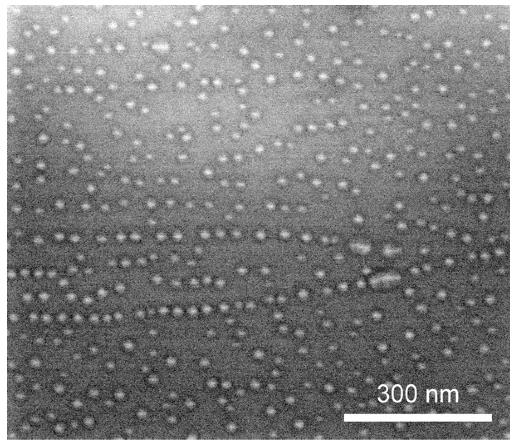
The reference sample was studied in FEI Nova Nanolab scanning electron microscope (SEM) and NT-MDT Ntegra atomic force microscope (AFM) for the characterization of shape, size and surface density of uncovered QDs.
For PL studies, the samples were placed in a flow Janis ST-500 cryostat to control the sample temperature (TPL) in the range of 77–300 K. The PL was excited by a YLF:Nd+3 laser operating in the cw mode (λ = 527 nm). The laser power was varied in the range from 0.084 to 40 mW. PL signal was detected using an SOL instrument’s MS 5204i monochromator and a single-channel InGaAs detector using synchronous detection (SRS 830 Stanford Research Systems).
3. Results and Discussion
The QD growth conditions were chosen so that the surface density of QDs was sufficiently large to provide high PL intensity, but not too large to stimulate QD coalescence. It is commonly known that InAs dots arranged quite close to each other merge due to Ostwald ripening [
7,
11]. A value of the surface density of uncovered QDs that we observe after 30 s interruption at the growth temperature before quenching is 4.1 × 10
10 cm
−2 (
Figure 2). Meanwhile, the density of the coalesced QDs is found to be 3.8 × 10
8 cm
−2. An average diameter of uncovered QDs is 23 nm, and their average height is 5.5 nm. QDs with these parameters are typically supposed to have separate energy levels contributing to distinct peaks in the PL spectrum after the capping procedure [
14,
19].
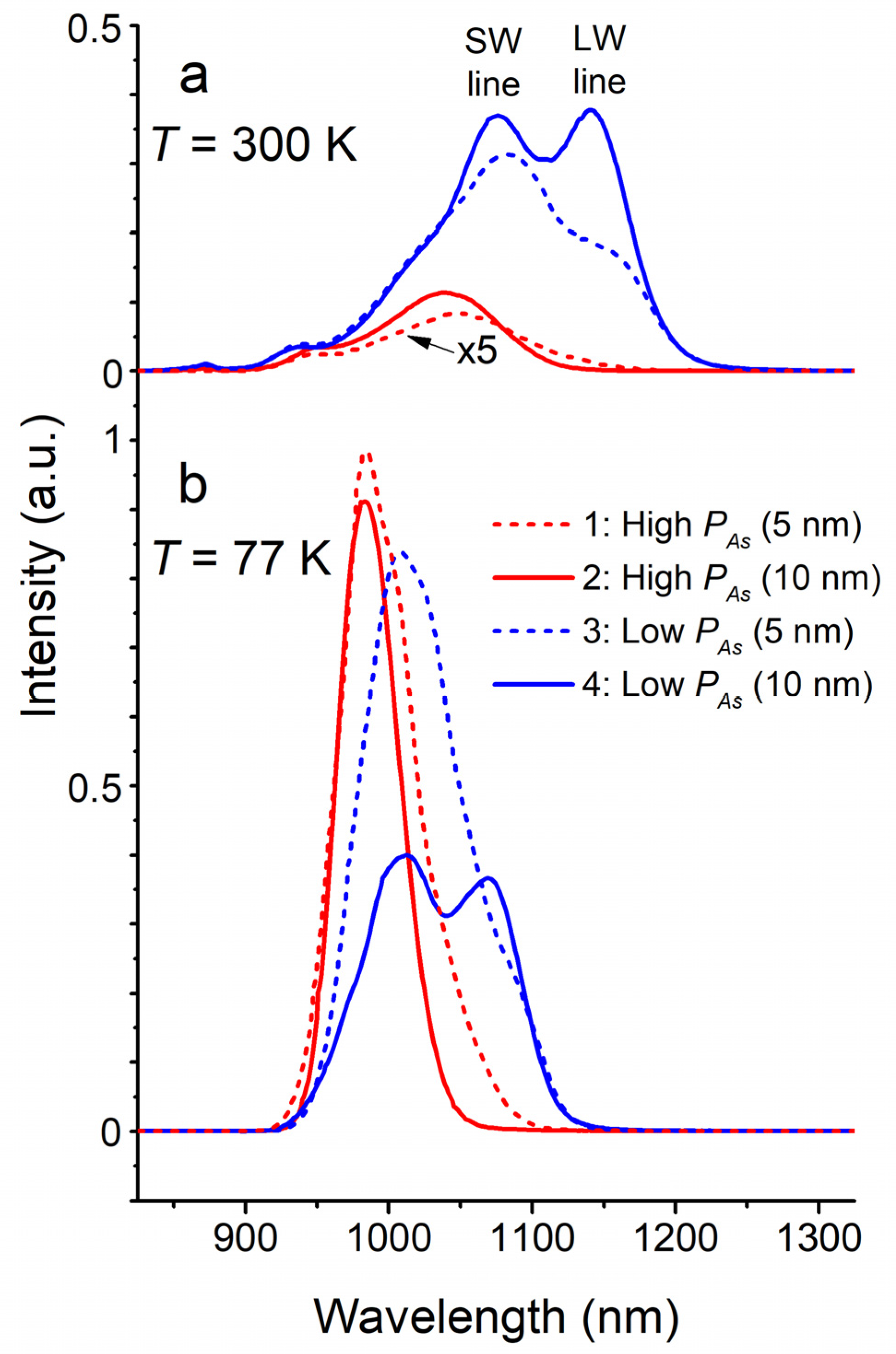
PL spectra taken from the overgrown structures demonstrate their strong dependence on the arsenic pressure used during overgrowth of QDs by the LT-GaAs layer (
Figure 3a). For each room-temperature spectrum, the lines corresponding to volume GaAs and InAs wetting layer are at ~870 and 935 nm, respectively, which is in good agreement with previous studies [
20]. However, longer-wavelength lines corresponding to the energy levels of QDs differ in their position and relative intensity (
Table 1).
When QDs are overgrown at
PAs = 3 × 10
−5 Pa, an unambiguous single broad line is observed in the room-temperature PL spectrum at 1049 and 1038 nm (shortwave (SW) line) for the LT-GaAs thicknesses of 5 and 10 nm, respectively (
Figure 3a), whereas at
PAs = 1 × 10
−5 Pa, two longer wave lines are pronounced. The first line (SW) is approximately the same for both LT-GaAs thicknesses and shifted to ~1080 nm. The longwave (LW) line is at a wavelength of ~1160 and ~1140 nm for 5 and 10 nm LT-GaAs, respectively. Although the appearance of an additional LW line is often attributed to an array of coalesced QDs [
11], we consider that its contribution is not sufficient to give a pronounced PL peak, taking into account the two-orders-of-magnitude-lower surface density of coalesced QDs compared with basic ones. Moreover, the coalescence of QDs before capping is equally inherent in each of the PL structures under consideration, but the additional LW lines appear only after the overgrowth at
PAs = 1 × 10
−5 Pa. Therefore, this behavior is not due to the initial size distribution of InAs islands, but to mass transfer processes during the overgrowth.
The red shift of the SW line, as well as the appearance of an additional LW line in the low-pressure LT-GaAs PL spectra, is due to the redistribution of the QD material and formation of new groups of QD sizes. At the high arsenic pressure, the diffusion of group-III atoms is suppressed, and therefore, InAs islands are predominantly conserved. Although the shape, size and composition of InAs QDs can change due to the indium segregation and strain-relaxing mass transfer, their uniformity in size is assumed to be retained. At the same time, an InAs QD covered by an intermediate InGaAs layer with changing In content is formed as a result of QD and LT-GaAs intermixing. As shown by TEM and X-STM studies [
11,
13], this form of QDs is typical for capping at the QD growth temperature. When the temperature is reduced to ultracold 300 °C, the QD shape remains almost perfectly pyramidal [
13]. Meanwhile, an increase in the temperature causes more intensive intermixing, which leads to blurring of the original pyramidal shape of QDs.
Similar behavior is observed when the arsenic pressure during the overgrowth is decreased. The diffusion length of group-III atoms increases, leading to more intensive mass transfer and coalescence of QDs located close to each other. As a result, two types of QDs appear in the volume and contribute to LW lines: 1140 nm for 10 nm LT-GaAs and ~1160 nm for 5 nm LT-GaAs (
Figure 3a). These lines are attributed to the appearance of QDs of quite a large size which contain an increased number of energy levels in the potential well, providing lower energy electron transitions with emission at longer wavelengths.
Integrated room-temperature PL intensity of QDs obtained at the low arsenic pressure during the overgrowth essentially exceeds the intensity of QDs which were overgrown at the high arsenic pressure (
Table 1). However, this difference is not so significant at 77 K PL (
Figure 3b). This indicates that excess arsenic accumulates in the capping layer grown at the high arsenic pressure and acts as additional nonradiative recombination centers for charge carriers migrating faster over the semiconductor volume at room temperature than at 77 K. It also should be noted that the integrated room-temperature PL intensity of QDs overgrown by 5 nm LT-GaAs is weaker than for 10 nm LT-GaAs, especially for the high arsenic pressure. It can be associated with higher defectiveness of thinner capping layers, which has been reported elsewhere. After the low-temperature overgrowth of QDs by a layer of 2–7 nm thickness, shallow depressions are formed above the tops of QDs and preserved on the surface at a stage of substrate heating up to a high temperature used for the overgrowth by a thick GaAs layer [
7,
11,
14,
17]. After the high-temperature overgrowth of the layer with these depressions, multiple dislocations are produced in the area above QDs [
7,
11]. In our study, the defectiveness of the structure increases when the 5 nm LT-GaAs layer is grown at the high arsenic pressure because, in this case, the excess arsenic incorporated into the thin capping layer (5 nm) desorbs, leading to the expansion of the depressions above QDs. Although the concentration of excess arsenic atoms decreases, an increased density of dislocations prevents efficient radiative recombination of carriers in QDs to a greater extent. However, the overgrowth of QDs by the thicker LT-GaAs layer (10 nm) allows inhibition of the depression formation and subsequent generation of dislocations [
11].
The intensity maximum of the LW line in the room-temperature spectra for the low arsenic pressure is observed to be higher than the intensity maximum of the SW line in the case of the 10 nm capping layer, but it is lower in the case of the 5-nanometer-thick layer (
Figure 3a). The integrated PL intensity from QDs overgrown by the 10 nm layer is also higher than from QDs overgrown by the 5 nm layer (
Table 1). This behavior can be explained by the difference in the surface density of QDs of various sizes formed during the diffusion of In atoms within the overgrown layer mixed with the QD material. In the case of the capping layer of a smaller thickness (5 nm), as noted earlier, a greater number of dislocations are formed in the layer after the high-temperature overgrowth than in the case of the overgrowth by the thicker LT-GaAs layer (10 nm). As a result, the integrated PL intensity at room temperature decreases, as does the intensity of the LW line, which corresponds to larger QDs having a greater number of dislocations in their neighborhood. Therefore, charge carriers in larger QDs are more prone to nonradiative transitions than in smaller QDs. This assumption is confirmed by the fact that the integrated PL intensity from QDs overgrown by the 5 nm layer increases with a decrease in the PL temperature to 77 K (
Figure 3b).
However, for the 10-nanometer-thick capping layer, the integrated PL intensity remains at the same level, with a slight decrease when moving from 300 to 77 K (
Table 1). As mentioned earlier, this indicates lower defectiveness of the material compared with the structure with the 5 nm layer. However, it is important to clarify the reason for the reduction in the integrated PL intensity from QDs at 77 K in comparison with the 10 nm layer. This regularity may be due to the continuation of intensive diffusion of In atoms at the stage of heating the 5 nm layer, which leads to an increase in the surface density of smaller QDs responsible for the SW line. Although the density of such QDs overgrown by the 5 nm layer is higher, the integrated PL intensity of QDs at room temperature becomes lower than in the case of the 10 nm layer due to the higher imperfection of the material. When QDs are overgrown by the thicker LT-GaAs layer (10 nm), the QD density remains almost unchanged during the heating, which is confirmed by the retention of two distinct lines in the PL spectrum (SW and LW lines).
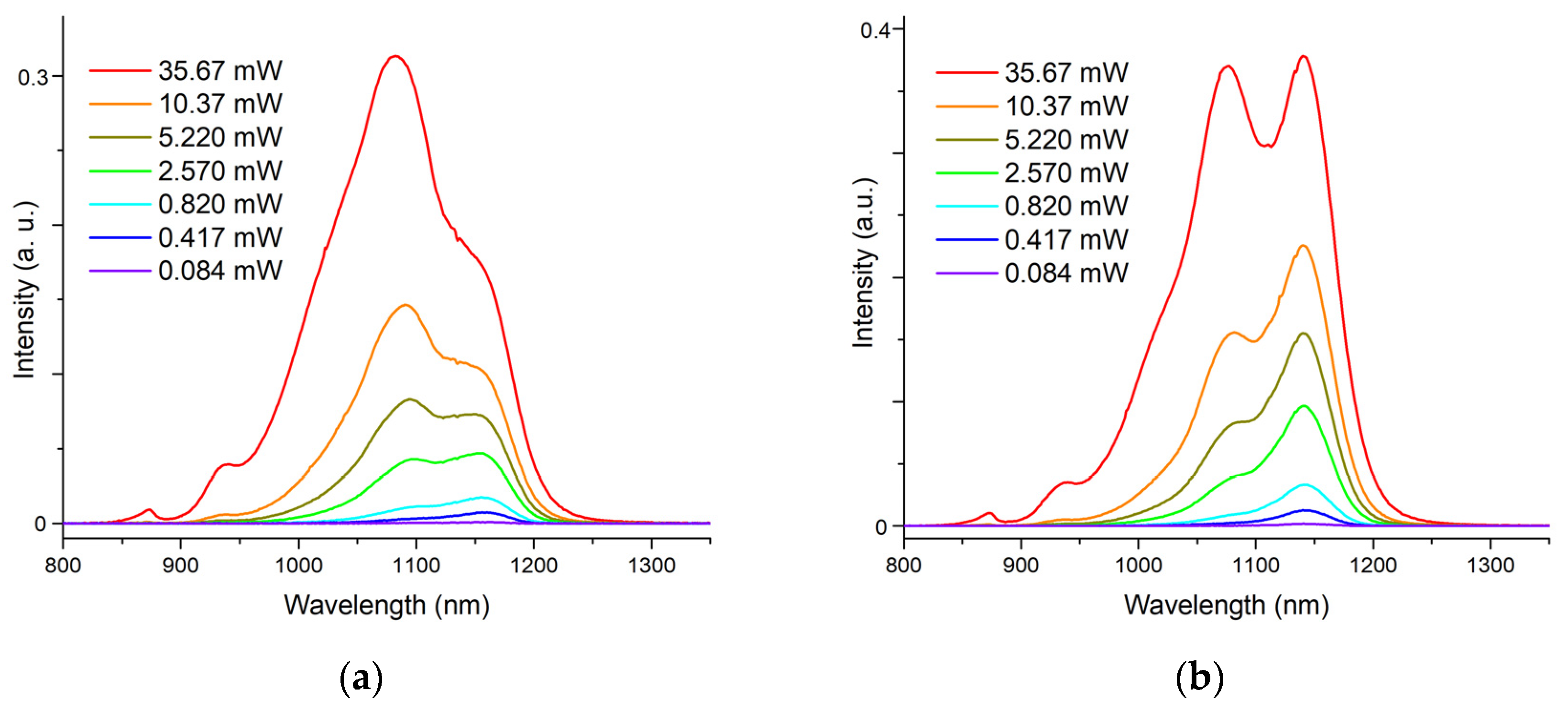
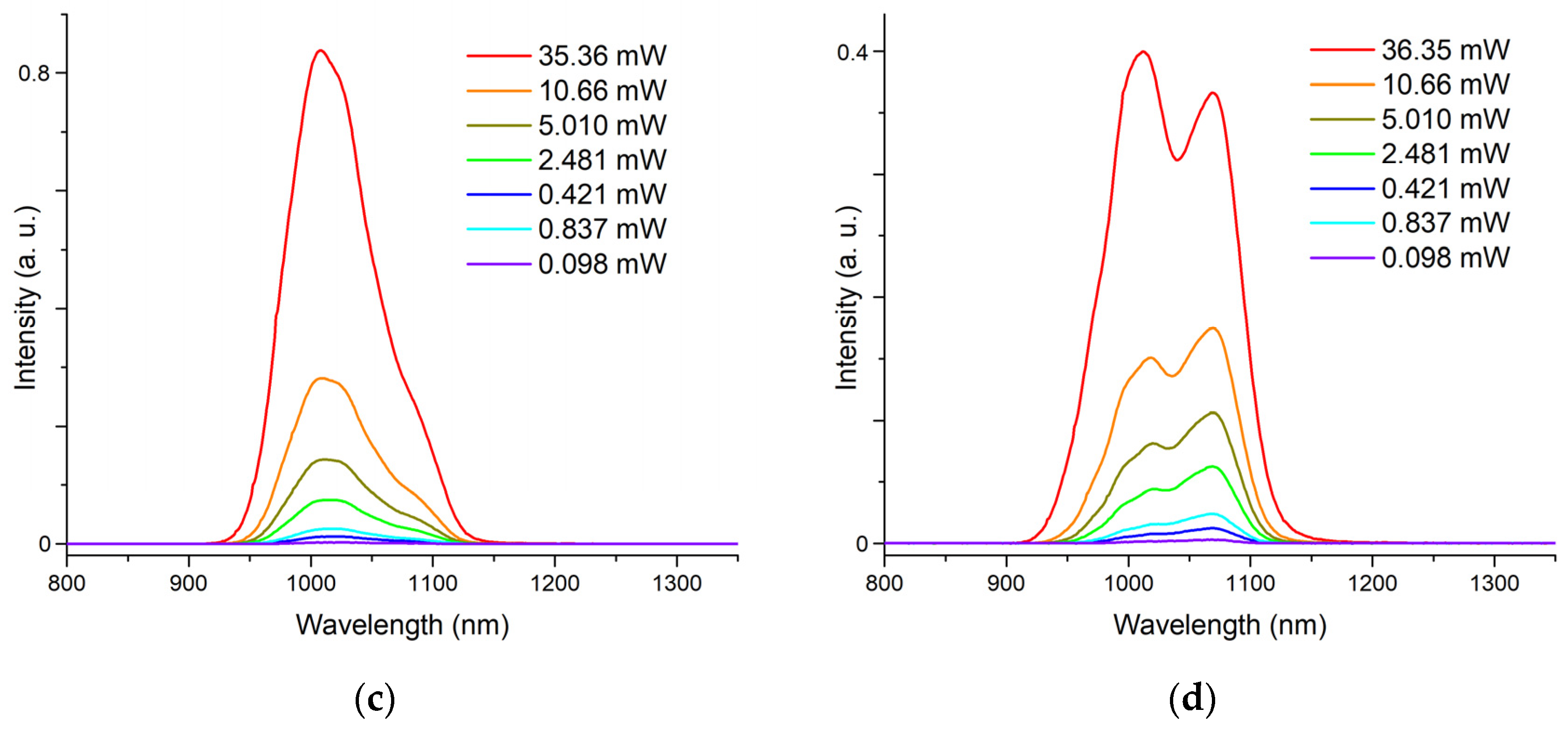
In order to estimate the nature of the separate SW and LW lines, the excitation intensity was varied in the range from 0.084 to 40 mW for the two PL temperatures of 300 K and 77 K for the samples with the low-pressure overgrowth by LT-GaAs layers of different thicknesses (
Figure 4).
For the room-temperature PL spectra of QDs overgrown at the low arsenic pressure, an increase in the ratio of SW to LW lines’ maximum intensity is observed, with increasing excitation power for both LT-GaAs layer thicknesses: 5 nm (
Figure 4a) and 10 nm (
Figure 4b). This is attributed to the fact that low-energy electron transitions in QDs of larger sizes are more favorable than shortwave transitions in smaller QDs. When the first ones reach saturation at a certain excitation intensity, the probability of high-energy transitions in smaller QDs becomes higher, contributing to the SW line of the PL spectrum.
A similar situation is observed in the cryogenic PL spectra, where the ratio of the SW to LW lines’ maximum intensity rises with increasing excitation power for the samples with both LT-GaAs thicknesses, i.e., 5 nm (
Figure 4c) and 10 nm (
Figure 4d). However, two LW lines become prominent at wavelengths of ~1020 and ~1080 nm. This fact confirms an assumption about the saturation of low-energy electron transitions, but it also demonstrates that appearance of a new group of QDs with an intermediate size (emitting at ~1020 nm) is possible in the case of the 5 nm LT-GaAs layer. Thus, the diffusion of In atoms within the thin capping layer is more rapid when the substrate heating occurs than within the thicker capping layer. Observation of both (SW and LW) lines in the cryogenic PL spectra at any excitation power confirms that the SW line is not due to the transitions from an excited level but due to the transitions in a certain type of small-sized QDs.
4. Conclusions
The influence of the arsenic pressure during low-temperature GaAs overgrowth of InAs QDs on their optical properties was revealed in this study. We demonstrated that overgrowth at a high arsenic pressure provides a single broad line in the QD PL spectrum, whereas two distinct lines are observed in the PL spectrum of QDs overgrown by the LT-GaAs layer at a low arsenic pressure. This behavior is explained by the strain-compensating mass transfer induced by the QD overgrowth. While the diffusion of In atoms is suppressed at the high arsenic pressure, formation of different size groups of QDs occurs during the low-pressure overgrowth. However, the integrated room-temperature PL intensity of QDs is significantly lower for QDs overgrown at the high arsenic pressure because excess arsenic incorporates into the capping layer in this case and leads to the enhancement of nonradiative recombination of charge carriers.
We also reveal a decrease in the integrated intensity of a thinner LT-GaAs capping layer (5 nm) as compared with a thicker layer (10 nm). We attribute it to one more source of nonradiative recombination centers, which has dislocations produced in the area of QD tops. These dislocations are caused by the formation of depressions during the low-temperature overgrowth and expand during the substrate heating of the thin layer (5 nm). Meanwhile, this pit formation can be inhibited using the low-temperature overgrowth by the thicker layer (10 nm). The higher defectiveness of the 5 nm LT-GaAs layer is also found for the overgrowth at the high arsenic pressure, which is associated with the desorption of the excess arsenic, inducing the depression formation.
The presence of the SW line at each excitation power in the cryogenic PL spectra for the samples with the low-pressure overgrowth confirmed the assumption that it is not caused by the electron transitions from an excited energy level, but it is due to the excitation of smaller-sized QDs. The SW line’s maximum intensity increases when the low-energy transitions from larger QDs reach saturation, giving rise to the shorter-wavelength transitions from smaller QDs. The analysis of the ratio of relative maximum intensities of the SW and LW lines also indicated a difference in the surface density of QDs obtained after the overgrowth by LT-GaAs layers of different thicknesses. Because the LW line’s intensity is relatively lower than the SW line’s intensity for the 5 nm LT-GaAs, we can conclude that the concentration of dislocations near larger QDs is higher than that near smaller QDs.


 ,
, 


