Article

Designing a Spintronic Based Magnetoresistive Bridge Sensor for Current Measurement and Low Field Sensing

1
Department of Electrical Engineering and Applied Physics, Transilvania University of Brasov, Blvd. Eroilor 29, 500036 Brasov, Romania
2
National Institute for Research and Development in Electrical Engineering, Splaiul Unirii 313, 030138 Bucharest, Romania
*
Author to whom correspondence should be addressed.
Electronics 2022, 11(23), 3888; https://doi.org/10.3390/electronics11233888
Submission received: 11 October 2022 / Revised: 20 November 2022 / Accepted: 22 November 2022 / Published: 24 November 2022
(This article belongs to the Special Issue Advanced Magnetic and Electrical Characterization Techniques)

Abstract

:
An exchanged-biased anisotropic magnetoresistance bridge sensor for low currents measurement is designed and implemented. The sensor has a simple construction (single mask) and is based on results from micromagnetic simulations. For increasing the sensitivity of the sensor, the magnetic field generated by the measurement current passing through the printed circuit board trace is determined through an analytical method and, for comparative analysis, finite elements method simulations are used. The sensor performance is experimentally tested with a demonstrator chip. Four case studies are considered in the analytical method: neglecting the thickness of the trace, dividing the thickness of the trace in several layers, and assuming a finite or very long conductive trace. Additionally, the influence of several adjacent traces in the sensor area is evaluated. The study shows that the analytical design method can be used for optimizing the geometric selectivity of a non-contacting magnetoresistive bridge sensor setup in single trace, differential, and multi-trace (planar coil) configurations. Further, the results can be applied for developing highly performant magnetoresistance sensors and optimizations for low field detection, small dimensions, and low costs.

1. Introduction

Measurement of the electric current is a key element in electrical systems, even more so with the continuous development and full-scale implementation of Industry 4.0 and 5.0 technologies in an Internet of things era. Some key characteristics can be identified for modern current measurement applications, such as high accuracy and sensitivity, linear response, DC/AC operation, low thermal drift, immunity to interferences, IC packaging, reduced costs, and power consumption.
Resistive-based current-sensing techniques are adequate for some applications but they present a lot of disadvantages, such as power loss, no galvanic isolation, and low bandwidth [1], issues that are not present with non-contacting current sensing techniques.
Typical non-contacting current sensor technologies are AC/DC current transformers, fluxgate magnetometers [2,3], or those that utilize Hall effect [4,5,6,7], anisotropic magnetoresistive (AMR) sensors [2,5,8], giant magnetoresistive (GMR) [4,9,10,11], and tunnelling magneto-resistance (TMR) sensors [12,13]. Current sensors based on magnetoresistive effects offer high accuracy, endurance, low temperature drift, low offset, and are suitable for low volume production together with tight integration capabilities with integrated circuits (ICs). An overview detailing their properties, performance characteristics, magnetic field behavior, as well as specific advantages and drawbacks was performed in [14,15]. Thus, for superior sensor characteristics (immunity to some electromagnetic interferences, high sensitivity, linearity), a double differential implementation of magnetoresistive current sensors should be used together with a multi-trace planar coil setup for improving low field response with a biasing system utilizing coils or permanent magnets. Versatility of the sensing system can be improved with a coil biasing system, but power consumption increases in this case.
Besides the general desirable characteristics for a sensor (sensitivity, low linearity error, low offset, and stability over time), in order to better define the requirements for a high performant current sensor, specific parameters for magnetic sensors have to be taken into account: hysteresis, perming, and geometric selectivity. Hysteresis is related to the magnetic material behavior and is usually defined as the current changing between the maxima of the full-scale range. Perming is the change in the sensor offset caused by a high intensity external magnetic field. Geometric selectivity refers to sensitivity of the sensor in function of the characteristics of the conductor through which the measured current is passing and the influence of crosstalk from non-measured currents or external magnetic fields [16]. Other practical characteristics are desirable, depending on the application in which they are implemented: immunity to high electric field variations, frequency response from DC to MHz, cost, weight, and size requirements.
The electrical resistivity of magnetic thin films (usually Fe, Co, Ni, or alloys like Permalloy—Ni80Fe20) is anisotropically dependent on the direction of the applied magnetic field [17]. Thus, the layer resistivity depends on the angle between the magnetization and direction of current flow. Moreover, the magnetization rotation direction and angle depend on the applied external field’s amplitude. The electrical resistance change can be measured as roughly the square of the cosine of the angle between the magnetization and the direction of current flow. This constitutes the basis for effects such as planar Hall effect (PHE), which is a consequence of the AMR effect.
Regarding the layout of AMR sensors, the basic approach is to utilize several magnetic thin film resistive elements that have a large aspect ratio (about 10 nm thin, a few μm wide, and tens of μm long), such that the magnetization is aligned on the longitudinal (easy) axis, connected in a Wheatstone bridge configuration for increased thermal stability and sensitivity around zero field. The maximum sensitivity and linearity are achieved when the magnetization is at 45° with respect to the current direction. This is commonly achieved using the Barber pole biasing technique [18] or other biasing techniques, such as herringbone [19].
In terms of classification, AMR sensors can be divided into two classes: those that are similar to Hall sensors and AMR bridges. [20]. The first class are those that share a geometry with Hall sensors, where the current is injected along one direction in the sensor cross and the voltage is measured orthogonally, these are referred as PHE sensors. In the second class, the AMR elements are combined in a Wheatstone bridge, such that the current is injected along one direction and the voltage is measured in the orthogonal direction. To further differentiate between the two classes, the term “PHE bridge (PHEB) sensors” was introduced to distinguish between other AMR bridge sensors, the more correct term being “exchange-biased AMR bridge sensors [21]. A comprehensive study for the geometry influence and structure of AMR/PHE sensors was performed in [22].
We demonstrated that both DC and AC currents through linear stripes can be measured down to μA using GMR sensors [15], however, some limitations in terms of sensor sensitivity, size, and setup complexity were found. For achieving lower detection limits, this study aims to consider some possible sources of electromagnetic interferences and trace current dimensional effects that can have adverse effects on the response of the magnetoresistive sensor. An analytical method can be used to estimate the response of the sensor, but such an approach is dependent on the number of dimensional parameters that are taken into account when modeling the magnetic field in the sensor area. This can be especially important for low currents which are producing magnetic fields that have to be measured. The method implemented in [15] did not take into account the length or thickness of the trace or specific trace geometries.
This work aims to improve the analytical method from [15], to include trace length and thickness as dimensional parameters. A comparative study is performed with different versions of the analytical method and finite elements simulations with COMSOL Multiphysics to study the influence of trace geometry and sensor placement on the magnetic field intensity in the sensor area. Results are applied for the design and implementation of a proof-of-concept exchange-biased AMR bridge sensor: often called planar Hall resistance (PHR) in the literature. The mode of operation of the sensor is proven using multi-domain micromagnetic simulations. Focus is placed on design optimizations by sensor placement and trace configurations that can be applied for various non-contacting current sensors. Experimental results from the PHR bridge sensor setup and a previously implemented GMR sensor setup are performed to validate the results. The main purpose of this study is to serve as the basis for designing optimized magnetoresistive sensor designs, improved mostly through geometric selectivity and experimental setup.

2. Materials and Methods

Materials and methods is structured into several sections. Firstly, the basic principles of the AMR, PHE (Section 2.1), and GMR effects (Section 2.2) are detailed, which are utilized in the experimental setup. Secondly, the analytical method for estimating the magnetic field intensity in the sensor area by a single or multiple printed circuit board (PCB) traces through which a current is flowing is shown in Section 2.3. Section 2.4 describes the layout of the PHR bridge sensor and critical analysis is performed using a single domain and multi-domain micromagnetic method to justify the specific layout influences for the sensing elements as well. Section 2.5 and part of Section 2.6 show the influence of thermal and magnetic annealing processes on the sensor performance to optimize sensitivity of the sensors. Exchange bias field effects on sensor response are justified throughout Section 2.4 and Section 2.5. Finally, Section 2.6 also describes the experimental setup and manufacturing steps for the demonstrator chip. Various sensor design steps and best practices can be extracted from all sections.

2.1. Principle of Operation–AMR and PHE Effects

The AMR effect appears in ferromagnetic bulk materials or thin films from Ni, Co, Fe, and their alloys [23]. The AMR effect comes from the dependence of the electrical resistivity of a material on the angle between the direction of electric current and direction of magnetization inside the material. In other words, the physical origin of AMR can be attributed to the anisotropic s–d scattering of electrons due to the spin–orbit coupling on 3d orbitals of ferromagnetic materials. [24,25]. The result of this effect is that in most magnetic materials, the resistivity of the material increases when the direction of the current is parallel to the applied magnetic field and minimum when the direction of the current is perpendicular. The AMR ratio can be expressed by:
Δ ρ ρ = ρ ρ ρ
where both resistivities ρ and ρ are expressed at saturation field, parallel, and perpendicular to the current direction, respectively.
Usually, for magnetic materials, this ratio is not larger than 5%, while for typical ferromagnetic NiFe films, the AMR value is in the order of 2–2.2% for magnetic fields of a few Oe [12]. Commonly, Ni80Fe20 (Permalloy) is used due to close to zero magnetostriction constants in all directions. For a schematic representation of the AMR effect, we can consider a thin film of ferromagnetic material (Figure 1). Note that for actual devices, an easy axis of magnetization is defined through the shape anisotropy (l > w) and the uniaxial anisotropy field HK. If an electrical current passes through the film along x direction and the magnetization, M, which makes an angle θ with the current, the longitudinal, Ex, and transverse, Ey, components of the electric field can be derived by considering the angular dependency of the resistivity tensor components ρxx and ρxy [7,18]:
E x = j x ρ x x = j x ρ + j x ρ ρ cos 2 θ
E y = j x ρ x y = j x ρ ρ sin θ cos θ
with j = j x and ρ and ρ as defined above.
The variation of the longitudinal resistivity, given by ρxx and measured through Ux = Ex × l, characterizes the AMR effect. The second term, Ey, shows generation of a signal perpendicular to the current direction in a geometry typical for Hall effect but with the applied field contained in the film plane. This is the PHE signal, VPHE, which is also defined in Figure 1:
V P H E = l ρ ρ t sin θ cos θ

2.2. Principle of Operation–GMR Effect

The GMR effect takes place in multilayered magnetic structures of the type FM/NM/FM coupled by exchange interaction. Here, FM denotes ferromagnetic layers of Ni80Fe20, Co, CoFeB layers with thicknesses between 1–100 nm and NM represents nonmagnetic layers, usually from Cu or Ag with thickness of about 1 nm, that mediate the exchange interaction between the FM layers. The basis of this effect is that a change in the electrical resistance of the magnetic multilayers is produced in response to an applied external magnetic field. The resistance change is dependent on the angle between the direction of the magnetizations of adjacent layers. Thus, when the ferromagnetic layers are magnetized in parallel, the resistance is at a minimum value, RP- while at antiparallel orientation, the resistance is at a maximum value. The electrical resistance dependency between the angle and direction of the electric current and the magnetization in the magnetic layers can be expressed by [26,27,28,29]:
R = R A P + R P 2 + R P R A P 2   c o s θ
Thus, for antiparallel configuration and parallel, we obtain:
θ = 180 °   c o s θ = 1   R = R A P = R H i g h
θ = 0 °   c o s θ = 1   R = R P = R L o w
The magnitude of the GMR effect is around 5–20% and is expressed by:
G M R = R A P R P R A P 100   % ,
The AA003-02 sensor was used in the experimental setup, which contains two active GMR elements, and two magnetically shielded identical sensors, together forming a Wheatstone bridge with an average sensitivity 25–40 μV/(V × A/m) [15,30].

2.3. Design Optimization of the Non-Contacting Current Sensor Based on Analytical Method for Current Stripes

Electromagnetic field modeling can offer great insight into the behavior, operation, and possible improvements for devices that rely on specific configuration of the magnetic field for proper operation, especially if these devices are susceptible to interferences or very high sensitivity is required. Applying software and mathematical methods for analyzing high-sensitivity magnetic sensors is a very a useful tool for improving their characteristics: reducing susceptibility to electromagnetic interferences, improving the signal-to-noise ratio, reducing size or costs. Several approaches from the literature have proposed modeling of the field produced by various configurations of single or multiple loops of wire in the same plane [31,32]. Most solutions focus on complex integral solutions that are usually solved with numerical methods [33], through FEM simulations [34], or serve application-specific purposes [35]. Although most methods that can be found in the literature are accurate up to a certain point, they are not adapted for the specificity required for field estimation in common setups in which magnetoresistive sensors are involved. However, many solutions shown in the literature, either lack automation or require intense computation steps. In this study, several specific optimizations are performed which reduce complexity significantly and do not require computationally intensive FEM simulations. For ease of use and integration with other instrumentation functionalities, the analytical method was implemented in a LabView application.
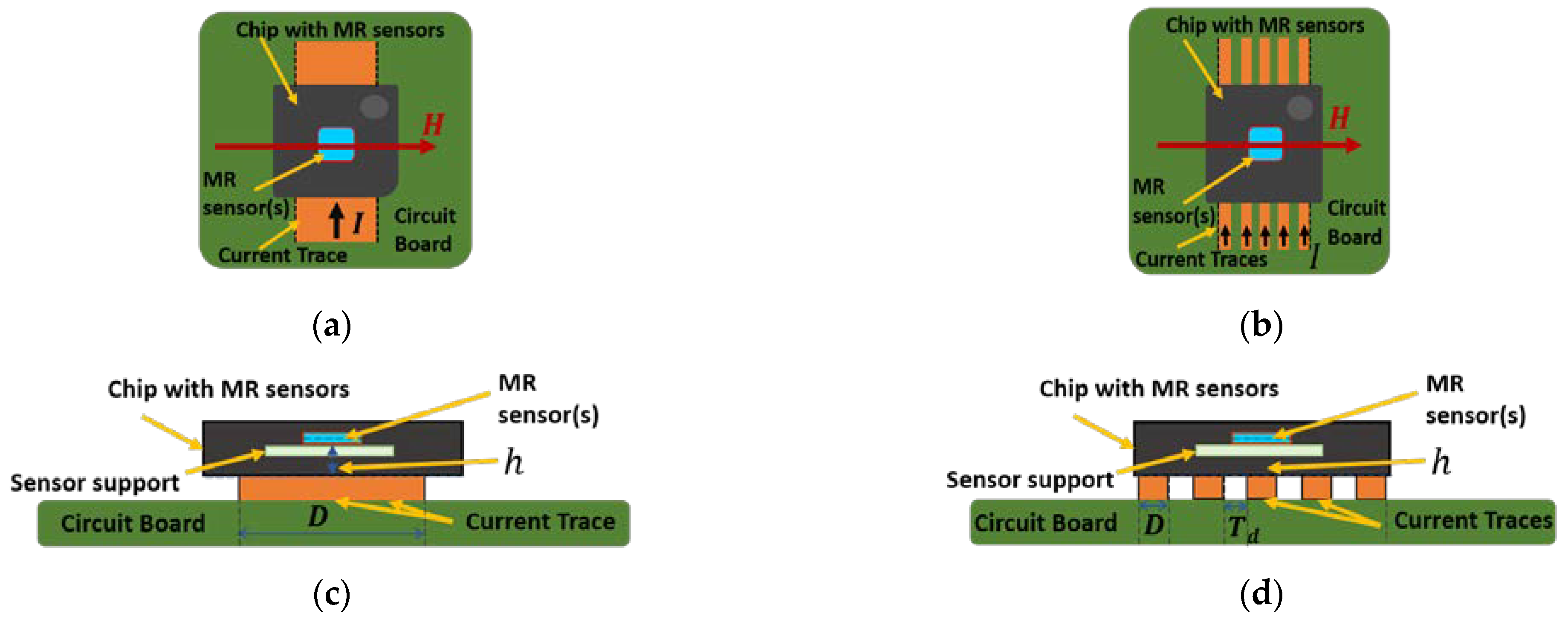
The basic principle of the proposed setup is to increase the intensity of the magnetic field in the non-contacting current sensor area, and thus the accuracy and sensitivity by a proper design of the current stripes from which the magnetic field to be measured is generated. This was achieved by integrating a planar coil below the magnetoresistive sensor which will increase the magnetic field intensity in the sensitive area of the sensor, essentially increasing sensor sensitivity for the same input current. In the current measurement setup, the MR sensors act as magnetometers, thus if a current, I, passes through a wire, the magnetic field, B, will produce a change in the output of the MR sensor. The working principle of the non-contacting current measurement setup for both single and multi-trace configurations is illustrated in Figure 2.
An approach optimized for low field detection by utilizing multiple current traces, in a double differential system, and implemented in a custom printed circuit board was demonstrated [15].
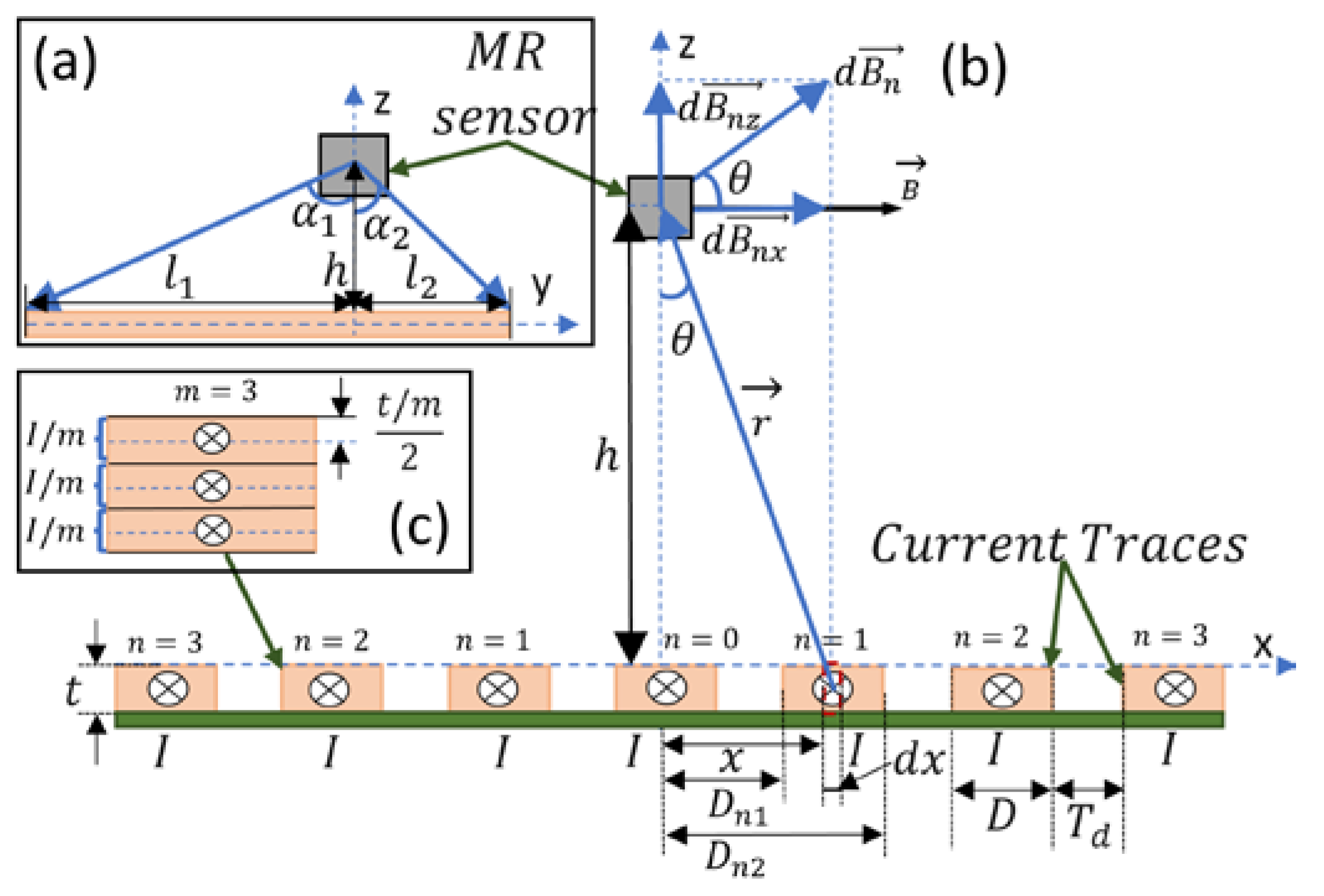
In order to estimate Bx, an analytical model based on Biot–Savart law was derived, which assumes that the sensor is centered above the multiple trace at distance h (Figure 3). Note that the thickness of each trace is divided by an m number of layers, consequently, h changes for each individual layer (from the center of each layer). For the finite length correction, we introduced the sum of the sine functions of the angles between the sensor area (above central trace) and for each end of the linear current trace (Figure 3a). Note that some geometric correction can still be introduced, especially for a large number of adjacent traces or nonlinear trace configurations.
For calculating the magnetic field, the Biot–Savart equation was applied to the geometry shown in Figure 3 and integrated:
d B = μ 0 I d l × r 4 π · r 3 100   % ,
By assuming a very long conductive trace (Figure 2d, the elementary current produced by the current I, can be expressed, using the Biot–Savart law by:
d B n = μ 0 d I 2 π r = μ 0 I d x D · 1 2 π h 2 + x 2   ; d I = I D d x ,
d B n x = d B n · c o s θ = μ 0 I d x 2 π D · 1 h 2 + x 2 ·   h h 2 + x 2   ,
where µ0 = 4π × 10−7 H/m is the vacuum magnetic permeability, D is the trace width, t is the trace thickness (not used in the equation), Td is the distance between the traces, h is the height on which the sensing element is placed above the trace, and θ is the angle shown in Figure 3a used to estimate the Bx component of the magnetic field.
By assuming a uniform linear current density, I/D, and integrating equation 11 from Dn1 to Dn2, the x component of the magnetic field generated by a trace n = 1, 2, 3,…, in the sensor area is determined corresponding for 2n + 1 traces for a planar coil (Equation (12)). If now, we introduce the length correction factor and divide the thickness of the trace in m layers, we get equation 13. If we take into account MR chip dimensions, usually the maximum value of n can be up to 6 (13 total traces).
B n x = μ 0 I 2 π D arctan D n 2 h arctan D n 1 h T ,
B n x = i = 0 m μ 0 I m 2 π D arctan D n 2 h i arctan D n 1 h i · s i n α 1 + s i n α 2 T
For a single trace (n = 0), from equation 13 it follows:
B 0 x = i = 0 m μ 0 I m π D arctan D 2 h i · s i n α 1 + s i n α 2 T  
A study based on four possible cases for this analytical method was performed: Case I- Infinite trace length, with a single layer (trace thickness neglected), Case II- Infinite trace length, with m = 35 layers (1 μm each layer), Case III, finite trace length, with a single layer (trace thickness neglected), and Case IV- finite trace length, with m = 35 layers (1 μm each layer). For Case II and Case IV, layered trace thickness means that the thickness of each trace is divided on a number of layers through which we assume a constant current, I/m is flowing (where m is the number of layers). The analytical method is in such a way implemented that the results of the final field is the sum of the field produced by the individual layers.
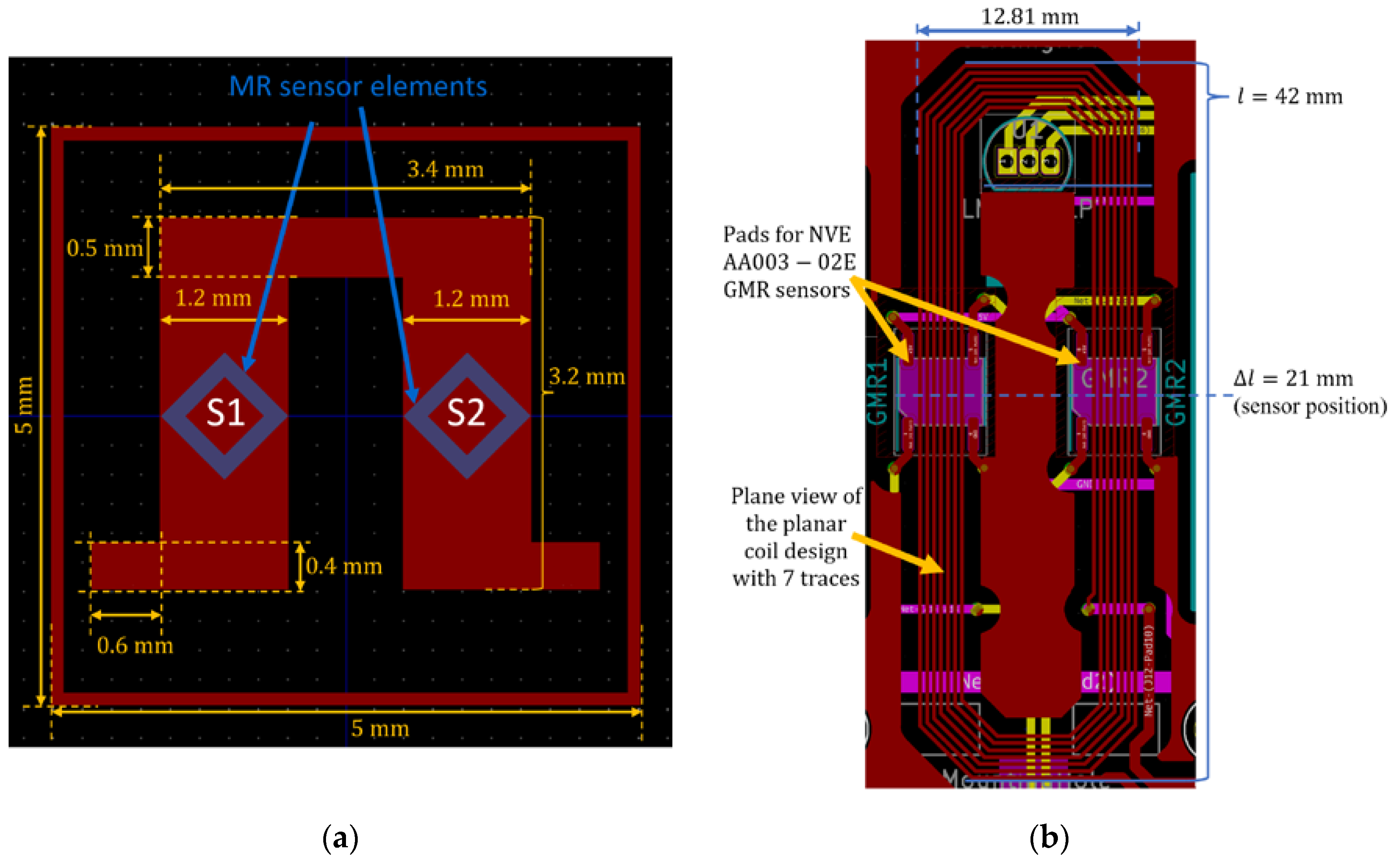
Moreover, for a comparative analysis of the results obtained with the analytical method, two use cases were studied using finite elements method simulations. Firstly, for a singular trace, results were compared with a single trace U-shaped current trace (Figure 4a) modeled to simulate the behavior in a double differential configuration. The specific dimensions of the U-shaped trace are chosen based on the ability to integrate highly sensitive and miniature magnetoresistive sensors, for example [36], in a double differential configuration in a very small package. Secondly, comparative analysis with experimental results is performed for the case of a multi-trace planar coil. The results of this comparison are shown in the Results and Discussion section.

2.4. Principle of Operation of the Exchange Bias AMR Bridge Sensor

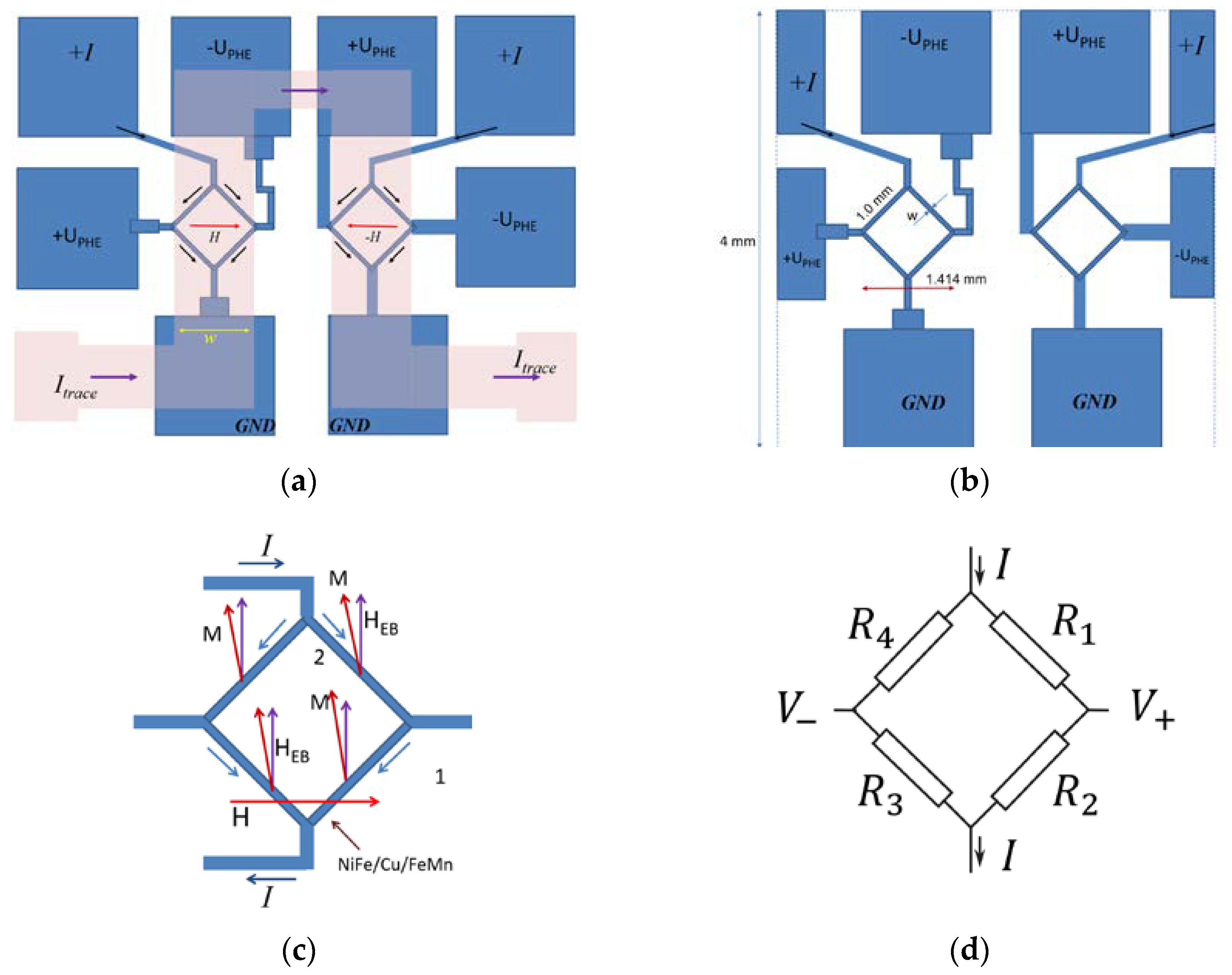
The design that serves as the layout for the demonstrator chip is shown in Figure 5. This design, which has two identical sensors is aimed at defining magnetoresistive structures adapted to the magnetic field produced by electric currents in the conditions of minimizing the effects created by temperature variations and interferences from external magnetic fields. The two sensors chip shows a double differential measurement system, in the sense that each of the AMR bridges is a differential sensor. On top of the sensor, a U-shaped Silver band is placed. The U-shaped trace was printed on top of a Kapton band with a thickness of 45 µm, by using a prototyping system (Voltera V-One) [37]. This band was placed on top of the sensors.
Based on the equivalent circuit for one AMR bridge sensor (Figure 5d), we can note that the four AMR chip elements are in a Wheatstone bridge configuration (arms of the bridge R1R4). Note that each resistor arm of the bridge can be constituted from multiple stripes for specific configurations [20]. Thus, the resistance of each arm is dependent on the number of stripes. If there is a positive applied current though the resistor, the output voltage (potential increase in the y-direction) from the bridge is:
V = I   R 2 R 3 R 1 R 4 R 1 + R 2 + R 3 + R 4 1 2 I R 3 R 1
where the result of the expression is valid when R1 + R2R3 + R4, thus when Istripe = I/2.
In [20], a single domain approach was used to model the response and field contributions on the resistance of a single stripe (in our case, equivalent to one arm of the AMR bridge). The expression that was obtained for the resistance of a single sensor construction element (single stripe) was:
R α = R 0 s i n 2 α S 0 B y e x t + S 0 B s f c o s α
where R0 is the stripe resistance when θ = 0 (θ is the magnetization rotation angle for a single domain stripe), α is the angle of a positive current passing through the stripe on the x-axis, S0 is the single stripe low field sensitivity, B y e x t is the field contribution due to homogenous external applied fields along the y-axis, and B s f is the contribution of the magnetic field induced by the bias current passing though the sensor (the self-field).
The single stripe low-field sensitivity S0 is [20]:
S 0 l Δ ρ w t B e x + B K
where w is the width, l is the length, t is thickness of the stripe, Δ ρ = ρ ρ , Bex is the exchange pinning field, and BK is the anisotropy field.
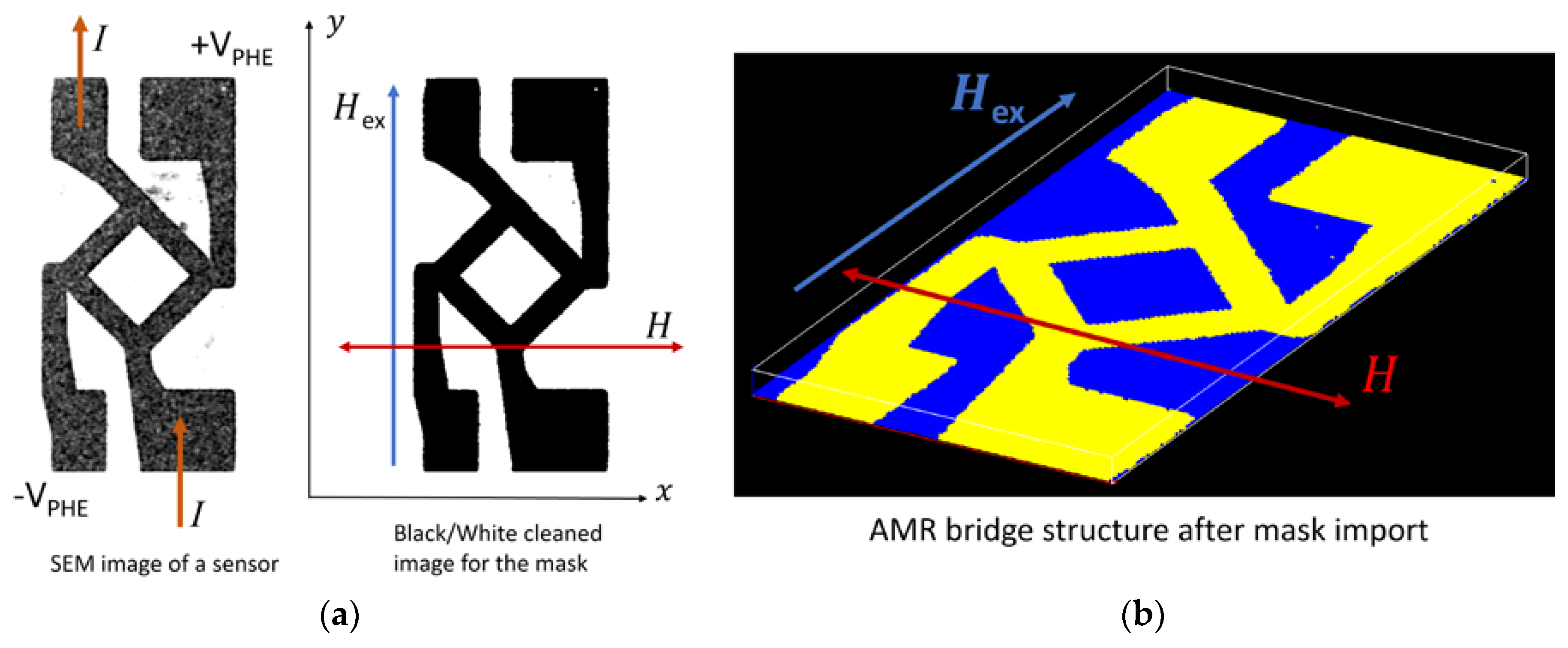
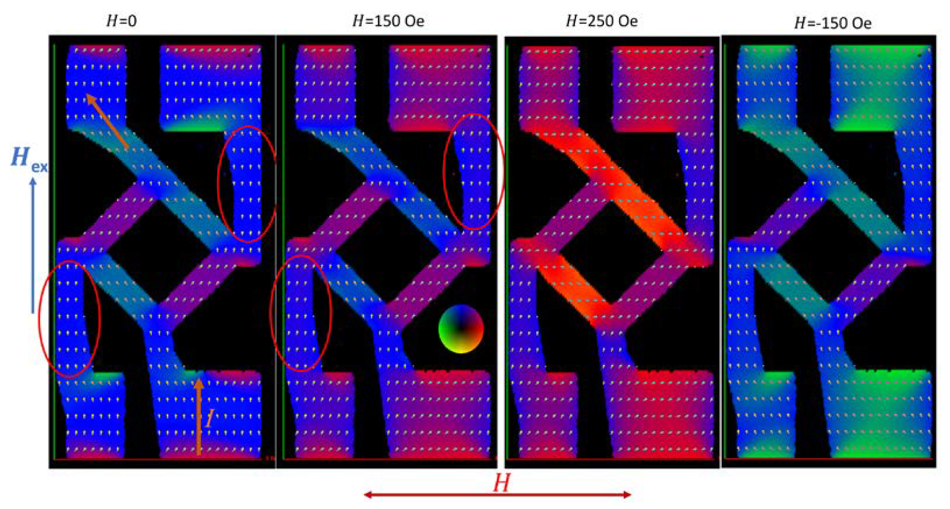
In order to validate the AMR bridge (PHR) sensor mode of operation for actual operation, we used a multi-domain simulation approach using LLG micromagnetics v4 [22,38]. The mask required for the simulation was obtained by editing a SEM image of the sensor and performing a black/white cleanup (Figure 6). The magnetic layer and spacing layer are situated in a 1000 × 2000 × 10 nm structure. The parameters used for the simulation are: saturation magnetization MS = 710 kA/m [14,22], exchange constant A = 1.3 × 10⁻¹¹ J/m, anisotropy constant Ku = 500 J/m3 [39], the exchange bias field (pinning field) Hex = 150 Oe, temperature T = 0 K; discretization cell 10 × 10 × 10 nm3. The convergence condition was maintained at 1 × 10⁻⁴. Note that between Ku and the anisotropy field Hk, there is the following relation HK = 2Ku/MS. Generally, micromagnetic simulators model structures at 0 K such that thermal fluctuations do not influence the results. These fluctuations make obtaining convergence difficult, especially for models with a high number of magnetic spins. Structures larger than 2 × 2 μm2 are usually not simulated because results are not significantly different and the computation time requirements are high. The magnetization distribution for different applied field values (H = 0 Oe, H = −150 Oe, H = 150 Oe, H = 250 Oe) is shown in Figure 7. From Figure 7 and the magnetization distribution along the x and y axis for the entire structure compared with the central area of the AMR bridge at low field values (Figure 8), it can be denoted that the contacting pads and traces have very little influence on the magnetization characteristic of the sensor as the magnetic moments of the vertical stripes almost do not change at different applied fields and thus no additional hysteretic behavior is added to the central area of the structure.

2.5. Fabrication of Exchange Bias AMR Bridge Sensor Demonstrator

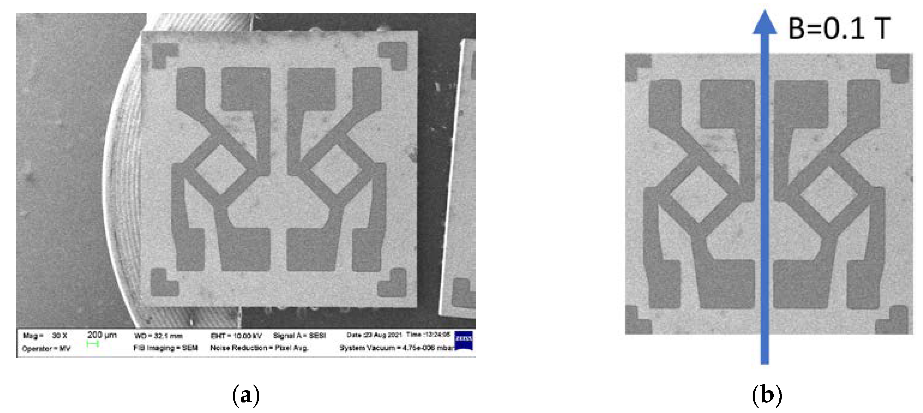
The AMR bridge sensors use spintronic structures of the type Ni80Fe20(10 nm)/FeMn(1 nm) and were deposited at ICPE-CA Bucharest though magnetron sputtering on an oxidized silicon substrate and microfabricated through the liftoff method. Given the particularities of the deposition method, the structures are amorphous and have a very low electrical conductivity. Additionally, the deposited structures do not show an established magnetocrystalline anisotropy axis or an exchange bias field, Hex, between the antiferromagnetic layer (FeMn) and the permalloy (Ni80Fe20) magnetic layer. Finally, 5 × 5 mm2 chips were cut. Of note is that a single mask was used for the chip, thus reducing complexity of the microfabrication process significantly. A scanning electron microscope image of the chip can be seen in Figure 9a. Several chips were thermally treated, Figure 9bc, with the purpose of enhancing the crystalline structures of the deposited layers and thus the electric conductivity. The thermal treatment was made in an argon (Ar, 99.99%) atmosphere, 2 mbarr pressure at a temperature of 450 °C for two hours [40].
The magnetic annealing system was comprised of: (1) Electronically controlled heated air blower (40–300 °C), (2) Vacuum pump (2 mbarr), (3) Electronic thermometer with K-type thermocouple; (4) Support Copper (Cu) sheet at the end of which a chip is fixed for the magnetic annealing, (5) Stainless steel tube connected to the vacuum pump, (6) Neodynium permanent magnets. The chip is placed at the end of a copper sheet which is introduced into a stainless-steel tube, which is connected to the vacuum pump. Given the small volume, a 2 mbarr pressure is obtained in approximately 15 min. Initially, the system is not placed between the poles of the magnets. After 15 min of vacuum, tube (5) is heated to 100 °C with the air blower for 10 min, in order to degas the interior walls, the Cu sheet, and the probe. The temperature is increased to 200 °C and the system is introduced within the poles of the magnets which generate a field of B = 0.1 T in the area of the tip of the tube where the chip is located. The temperature is maintained for 5 min after which it is dropped to 30 °C within 10 min. Field measurements were made with a Lake Shore 475 DSP Gaussmeter.
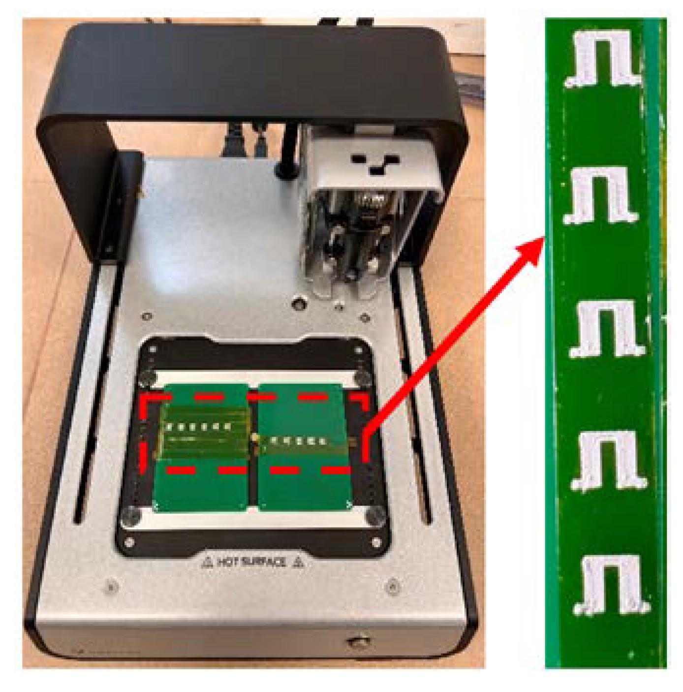
In order to produce the U-shaped current trace, Figure 4a, on the surface of the sensor, the utilized method was to print directly on a Flexible Kapton band, with silver ink, Voltera Adorable Anchovy, Flex 2 ink type [41], which remains flexible after thermal treatment for eliminating organic compounds. This ink is kept between 4–10 °C and is also compatible with polyethylene terephthalate (PET) and other flexible polymer substrates. The resistivity of the ink is around 1.36 × 10⁻⁷ Ωm after thermal treatment. The U-shaped trace was realized utilizing the dedicated PCB printer, Voltera V-One, Figure 10 [37]. A 6 mm wide and 45 µm (micrometer measured) Kapton band was used. For maintaining mechanical integrity and flatness during printing, the Kapton tape was temporarily fixed on a standard FR4 PCB board. The printer was configured to print a 35–40 µm layer from a distance of 0.08 mm from the surface and for the printing head, a 150 µm metallic tip was used. Immediately after printing, the entire ensemble was thermally treated at 160 °C for 30 min. By using a scalpel, a strip containing a single trace was cut and placed on the surface of the sensor. On the ends of the U-shaped trace, two wires were bonded using silver paste. The electrical resistance of the conductive trace was measured with the Keithley 2700 digital multimeter using a 4-wire method: R4w = 0.096 Ω.

2.6. Galvanomagnetic Characterization of the Exchange-Biased AMR Bridge Sensor

2.6.1. Experimental Setup

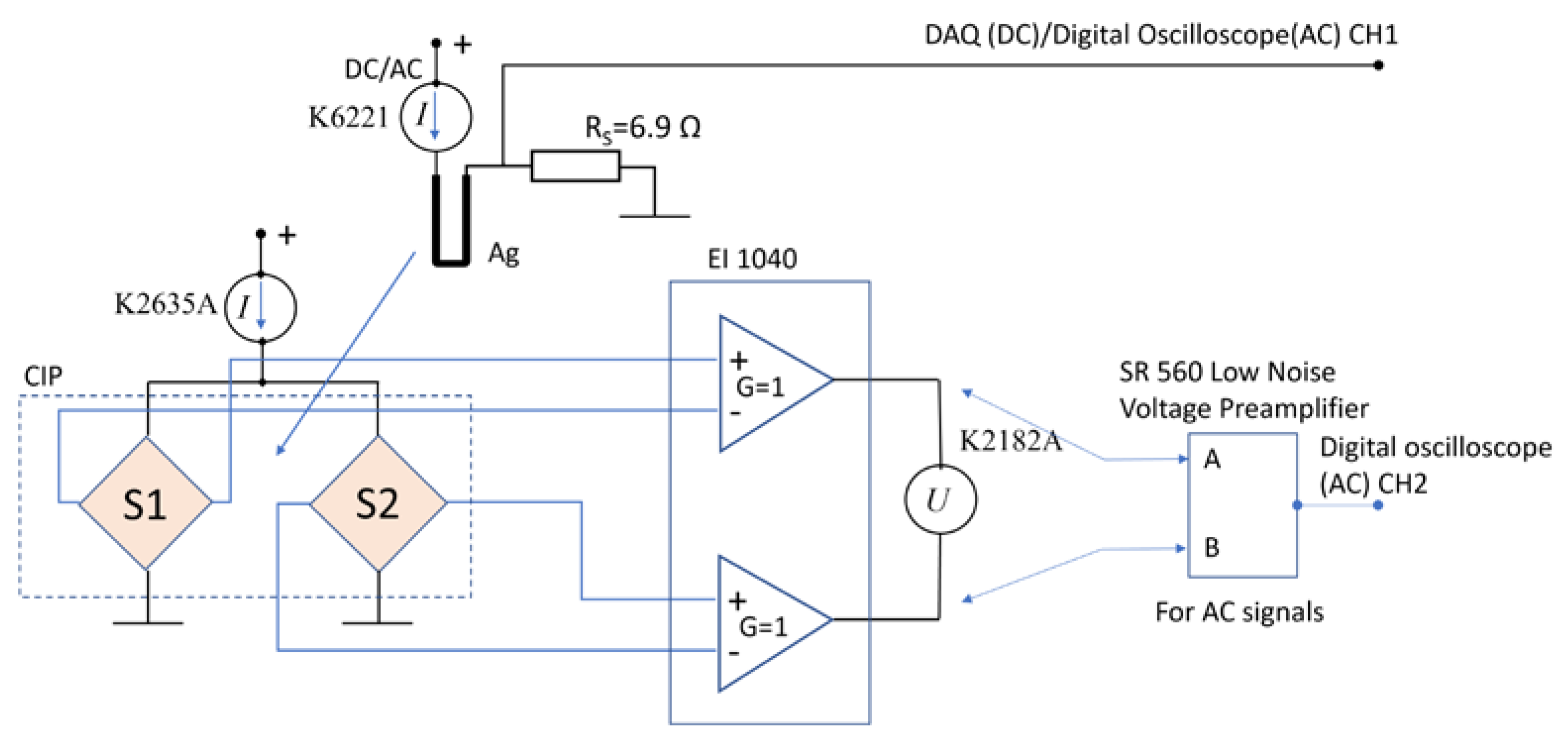
The functional block diagram of the setup can be seen in Figure 11. Evaluating the performance of the sensor is necessary as they should be able to detect low magnetic fields, under 1 Oe (10−4 T in air). Note that given the identical layout, results for a single sensor on the chip are shown.
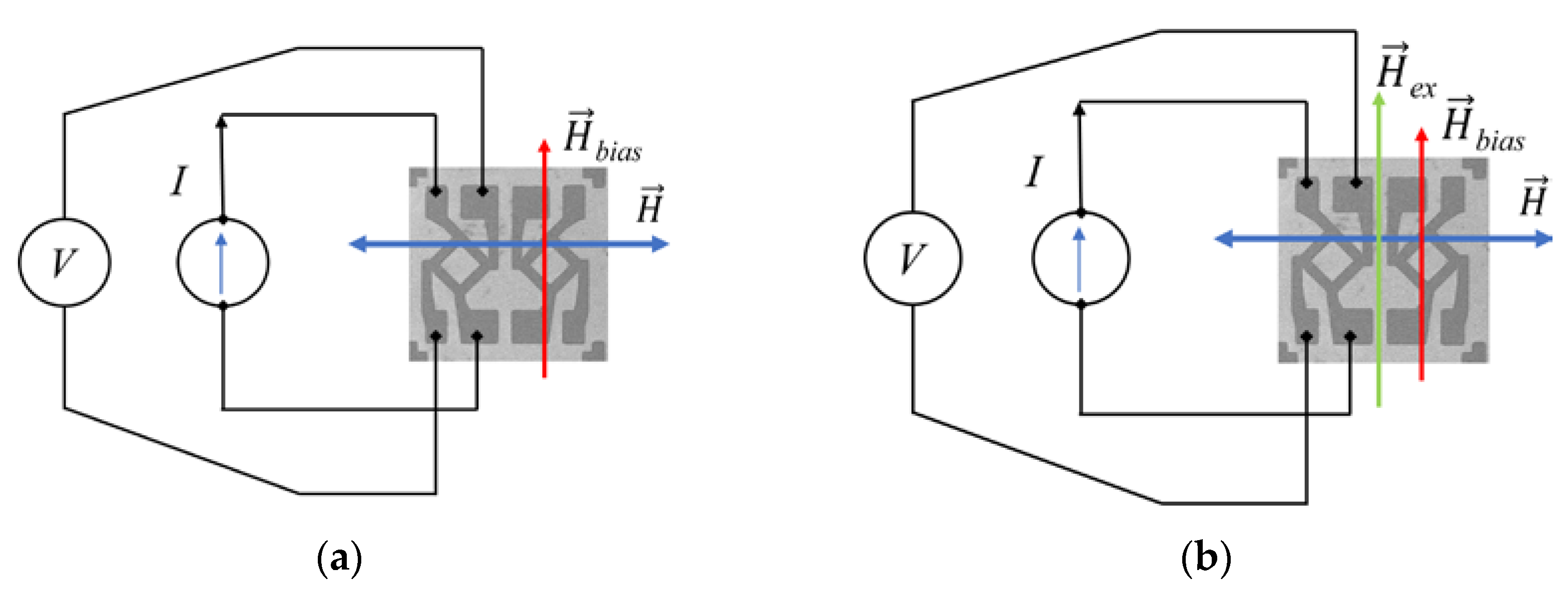
The chip measurement setup for both cases is shown in Figure 12. The magnetic field is applied in the sensor plane. A Keithley 6221 power supply is used to supply the sensors and a Keithley 2182 A nanovoltmeter for measuring the voltage output. As a magnetic field source, a Helmholtz coil was used, able to generate fields up to 200 Oe, which was powered by a programmable current source, Kepco BOP 100–10 MG. The coil was calibrated using the Lakeshore 475 DSP digital gaussmeter while data acquisition was done on a PC. For some tests, a biasing field was applied, Hbias, in order to linearize the characteristic of the sensor and to highlight the necessity for magnetic annealing; H is applied on the direction of the field which will be generated by the conductive trace, Figure 5. The sensor was supplied with a 1 mA current, DC.
Before testing, the chip was contacted with silver plated Cu wires. The wire-bonding was done with Ag paste from Sigma-Aldrich with a 24 h curing time at room temperature. The contacted chip was placed on a connecting PCB board, SO8, MSOP8 which allows placement in a DIP PIN 8 socket with gold plated pins, Figure 13a. Over the chip, the printed U-shaped trace was placed. Thus, a compact structure was obtained, which can be considered a hybrid integrated circuit that can be manipulated and characterized to allow great versatility. A second U-shaped trace was placed beneath the sensor to show the setup implementation for higher currents testing. Since the response of the sensor for low field values is of interest, a small size Helmholtz coil system was placed next to the chip, Figure 13b. The entire setup is placed in a ferromagnetic enclosure for magnetic shielding. The chip was introduced in a DIP PIN 16 socket where necessary connections were made to the connection grid while remaining pins was used to connect the current traces. An additional two ferrite permanent magnets were used to compensate the effect of the exchange bias field, Hex (noted as Hbias, Figure 12b).

2.6.2. Characterization of the Demonstrator Chip—After Thermal and Magnetic Annealing

For comparison purposes, the field characteristics for a chip with only thermal treatment applied and for a chip that went through the magnetic annealing process are shown.
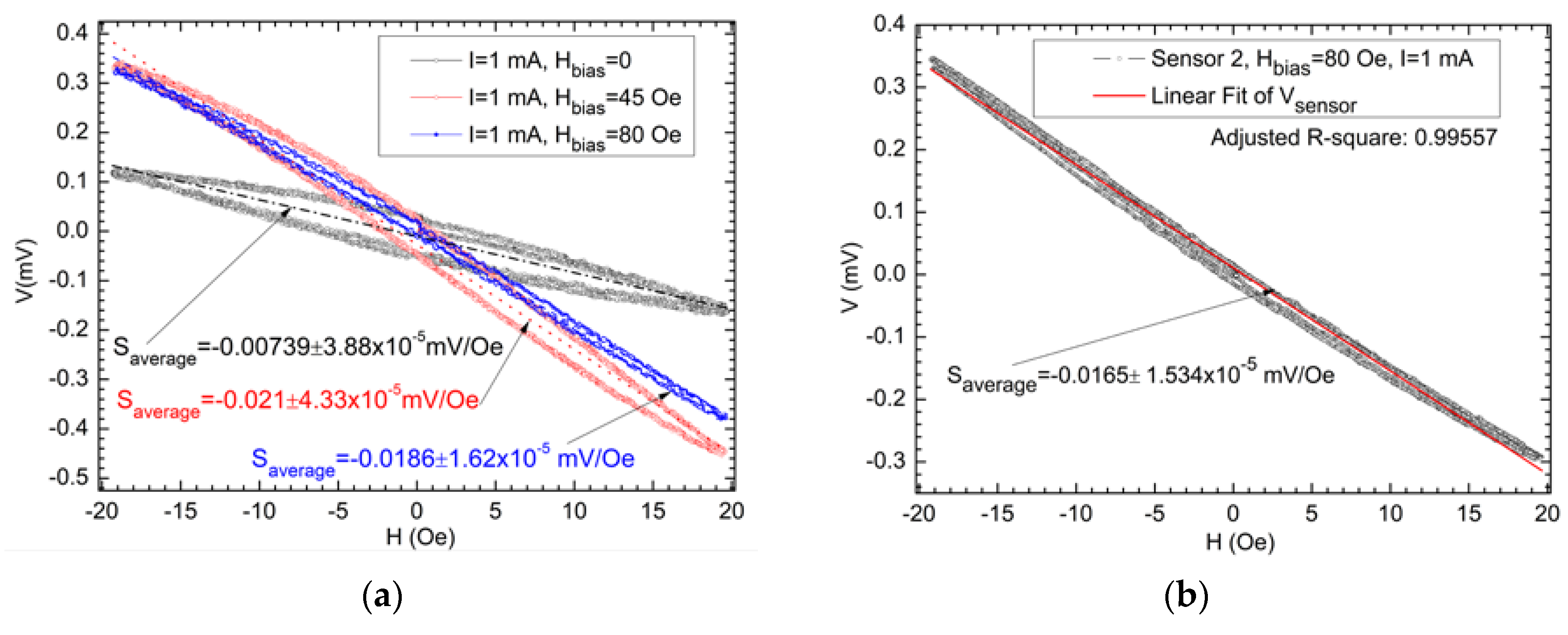
For the chip with only the thermal treatment, we can note, Figure 13a, the nonlinear, hysteretic characteristic, typical for AMR structures with no magnetic anisotropy and defined direction for Hex. By applying a prepolarization field, Hbias, like in Figure 12a, the nonlinearity of the response characteristic can be reduced, Figure 14b. This field has the same effect such as Hex which can be induced through magnetic annealing; HEB depends on the nature of the FM and AFM layers, the quality of the interface between these layers, and the magnetic annealing process.
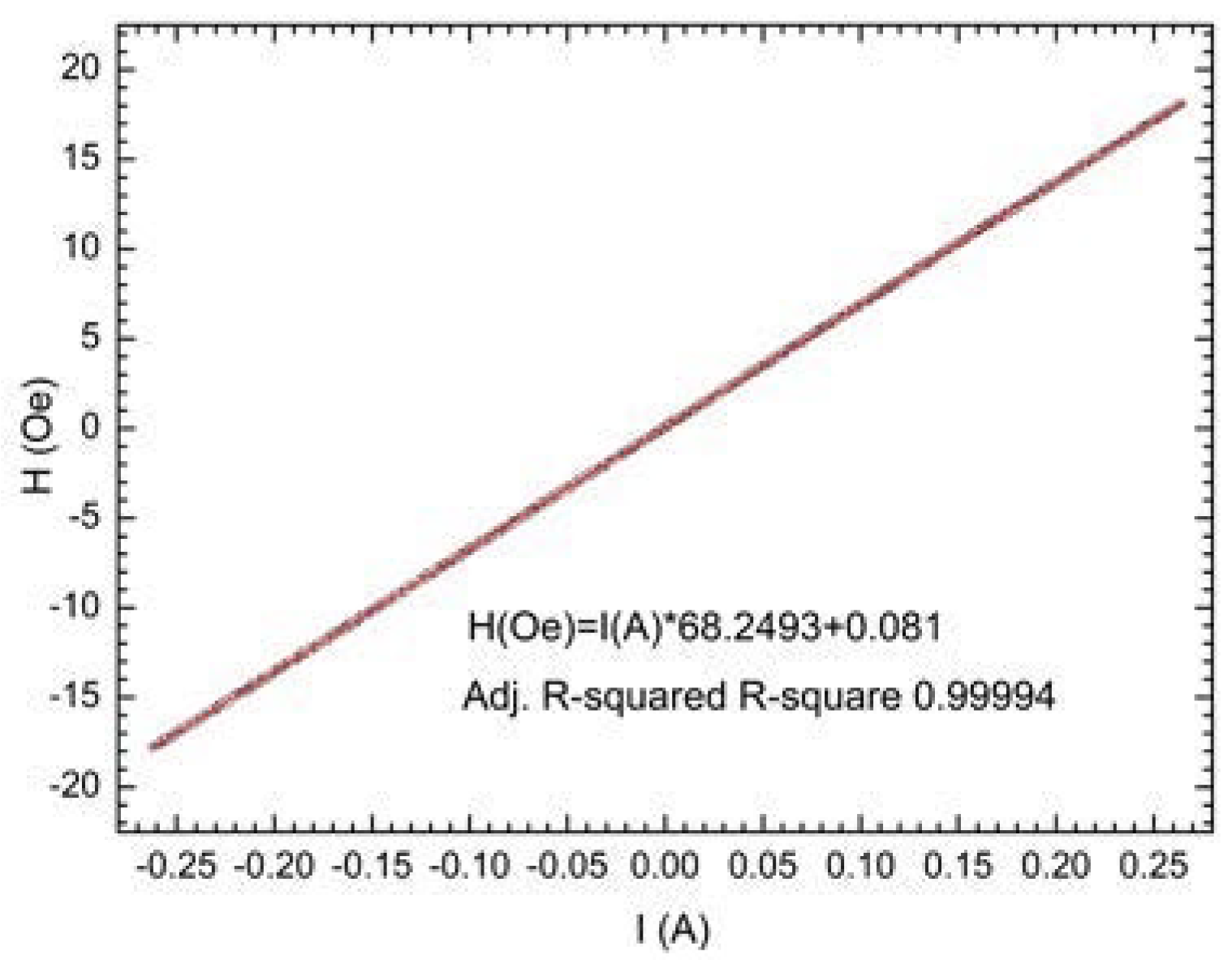
For the chip with both the thermal treatment and magnetic annealing, the results can be seen in Figure 14b for sensor “1”: and Figure 15b for sensor “2”, connected as shown in Figure 11b. The Helmholtz coils field characteristic (Figure 16) was obtained by placing, instead of the chip in the setup, the Hall probe of the Lakeshore 475 DSP gaussmeter.
By comparing the results from Figure 14a and Figure 15a, for Hbias = 0, we can note the emergence of the Hex field in the magnetically cured probe. In order to reduce hysteretic behavior and nonlinearity, two permanent magnets were placed on the wall of the metallic shielded box. Due to the box being ferromagnetic, the field from the magnets closes through it. Figure 15b shows the characteristics V = f(H) for two values of the biasing field Hbias = 45, respectively, 80 Oe. Additionally, the positions of the two magnets were modified such that a compromise is obtained between sensitivity and linearity. The Hbias = 80 Oe was considered optimal as higher values will reduce sensitivity. Note that the two sensors have a 1 mm gap between them. The light asymmetries between the response of the sensors will be compensated in the differential measurement system. By taking into account the distribution of the current through the U-shaped band and the magnetic field orientation created by the sensors, the output voltage will be of type: Vdiff = Vsensor1Vsensor2, as discussed in detail in [14,15].

3. Results and Discussion

3.1. Case Study Utilizing Analytical Model and Finite Elements Method Simulations for Currrent Stripes Optimization

For the finite elements method (COMSOL) simulation, a single trace “U-shaped” current trace was modeled (Figure 4b) to simulate the behavior in a double differential configuration. The specific dimensions of the U-shaped trace are chosen based on the ability to integrate highly sensitive and miniature magnetoresistive sensors. The specific parameters utilized for both the COMSOL simulation and the analytical model are shown in Table 1. Note, that in COMSOL, the U-shaped trace was modeled using Ag material properties but with a reduced resistivity of 1.36 × 10⁻⁷ Ωm to correspond to the experimental measurement, while the planar coil was modeled with Cu material properties with a resistivity of 1.72 × 10⁻⁸ Ωm. Note that the thickness of the U-shaped trace was 35 µm in the simulation for direct comparison with the planar coil thickness.
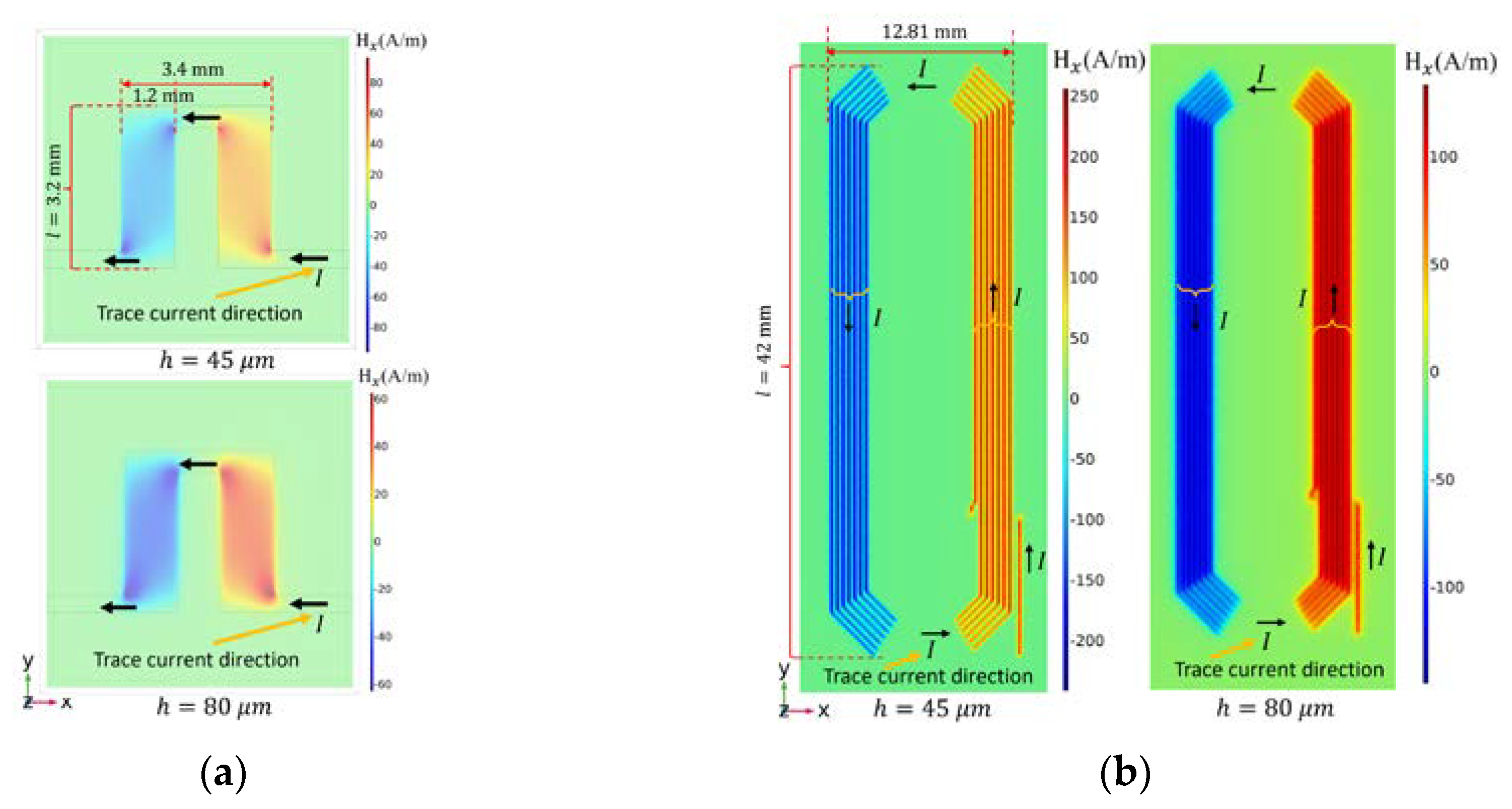
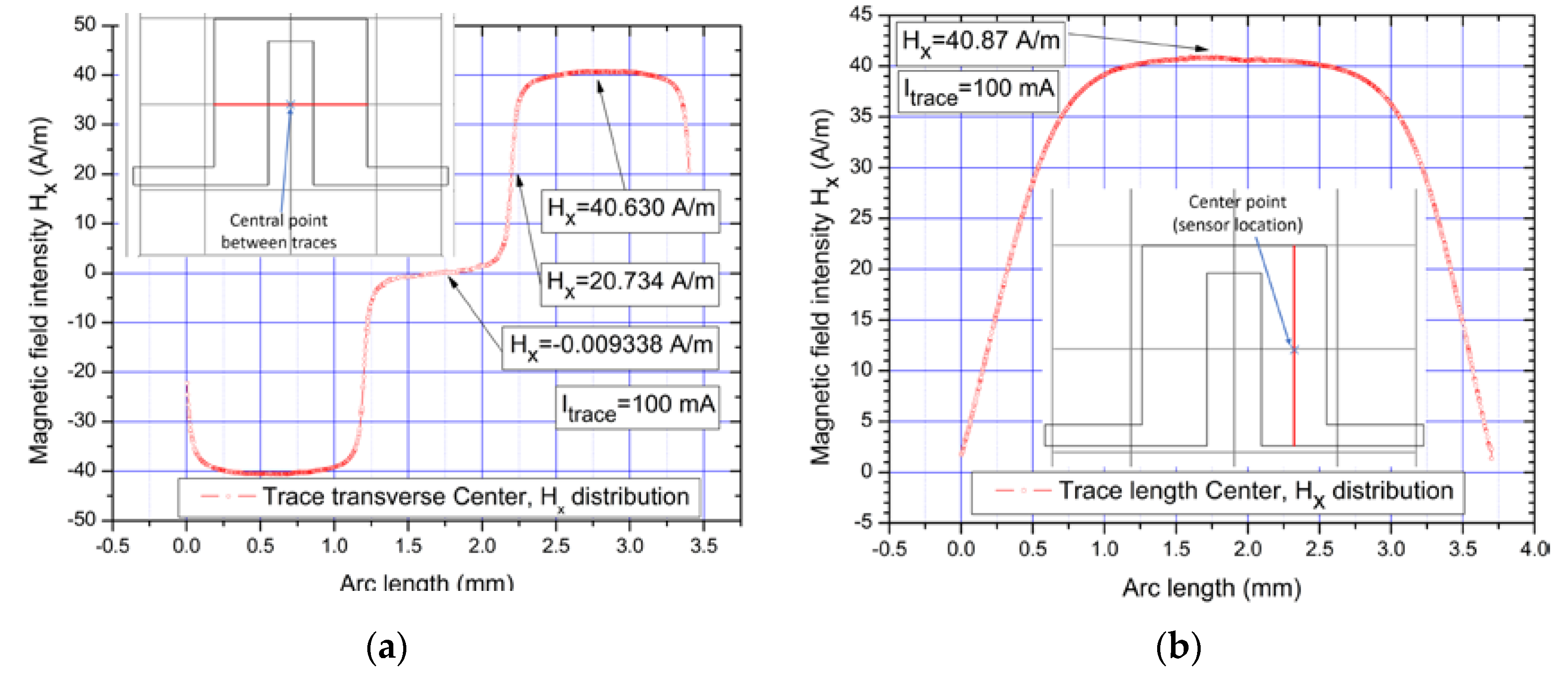
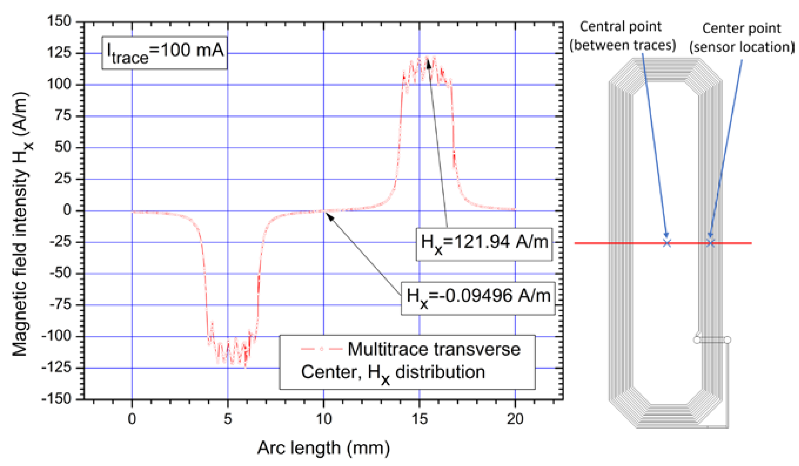
Figure 17a shows the magnetic field intensity distribution along the x-axis, Hx obtained from the COMSOL simulation of the U-shaped trace, and Figure 17b of the Multitrace from Figure 4b. In order to better illustrate the field values at specific points, at height h above the sensor, data were extracted for points of interest along transverse (Figure 18a and Figure 19) and longitudinal lines, Figure 18b (note the insets).
From Figure 18 and Figure 19, we can notice that, as expected, the magnetic field intensity is maximum at the center of the trace and there is a minimum magnetic field intensity between the traces. Figure 20a results show that the analytical model converges towards the COMSOL simulation results in the following way (for the U-shaped trace): for higher field values and consequently closer distance from the trace, the cases where a very long conductive trace is assumed (Case I and Case II) are closer to the results obtained from COMSOL while for the finite model (Case III and Case IV), results more closely converge to the results from the simulation at larger distances from the trace. Moreover, for the planar coil configuration, the analytical model provides results similar to the simulation for distances closer to the coil (Case I and Case II) while Case III and IV converge more closely at further distances which is the opposite behavior as in the case of just a single trace. We suspect some of the inaccuracies of the finite length models can be corrected by further geometric corrections. Additionally, more studies can be performed at various distances and trace configurations as the specific magnetic field at further trace distances can also contain y and z components, which can affect the sensor response, thus the analytical method can be improved to also account for those changes. Table 2 shows validation data for the central point (note inset from Figure 18a) between the COMSOL simulation results and the analytical method, after which the analytical method for the seven traces planar coil is compared with experimental results from [15]. The parameters from Table 1 were used for the results shown is Table 2. Note that the field values are calculated for 45 µm (thickness of the Kapton tape on which the trace is printed) and 80 µm distance between the sensor and the trace for the U-shaped trace and 0.8 mm or 0.08 mm for the planar coil as the planar coil experimental setup utilized the AA003-02 encapsulated sensors [31].
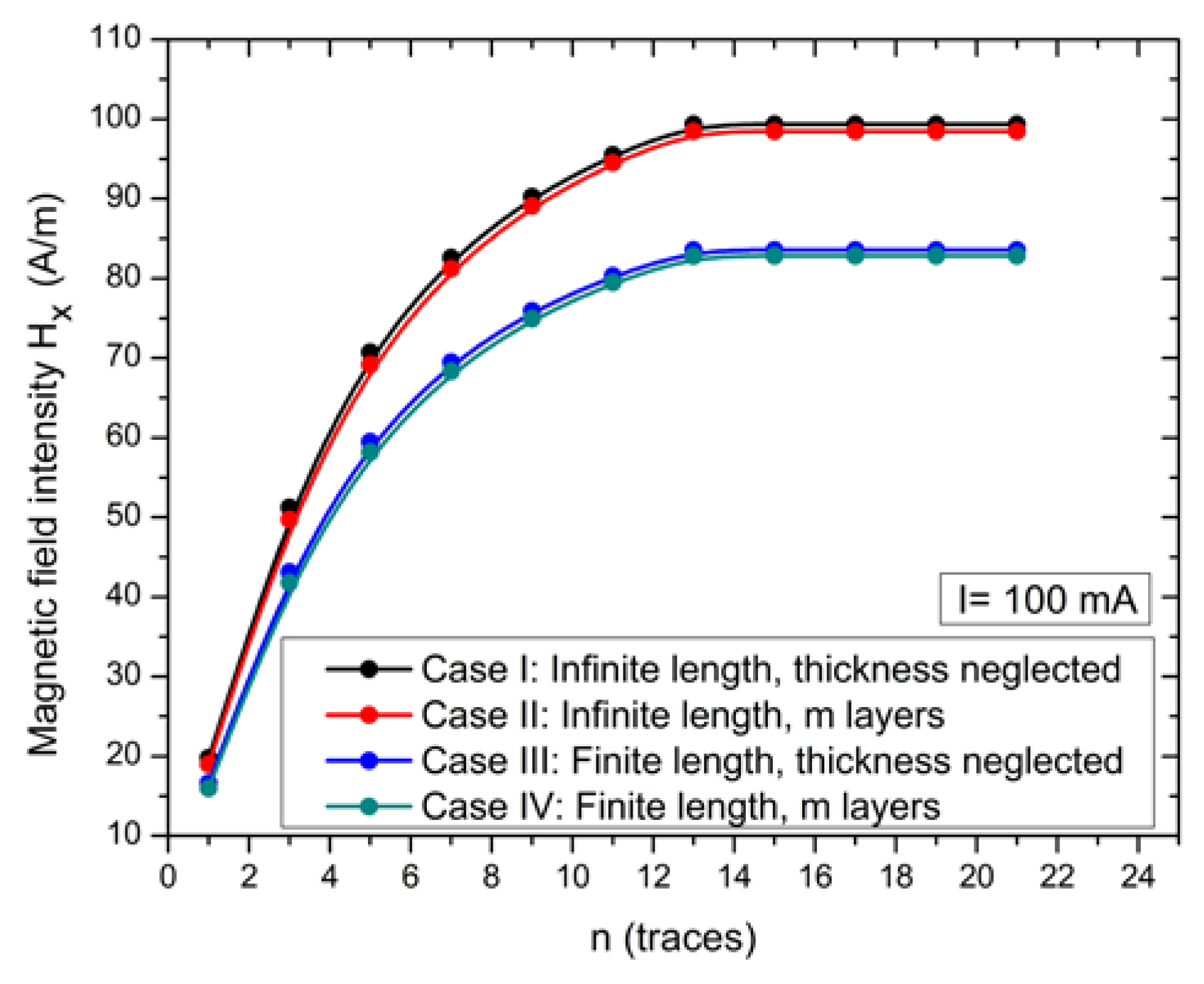
Figure 21 shows results obtained with the analytical method for a multi-trace configuration–different numbers of trace configurations (from 1 to 21 traces). We can denote, that the field intensity in the sensor area increases up until 13 traces, after which the field increase is minor. From tests, we determined that this number is consistent no matter the trace configuration of the planar coil (D, Td) and the current flowing through the trace. We consider that at a higher number of traces, other field parameters on the y and z axis also play a role in the field distribution, thus accuracy of the results can be affected with the current implementation.
By analyzing the data from Table 2, for the U-shaped trace, we can note that the estimated value of the surface parallel component of the magnetic field in the sensor area varies between 30 and 39.68 A/m (between 0.4 and 0.48 Oe), depending on the chosen model. Given that the U-shaped trace is a relatively short trace (3.2 mm), with a length/width ratio = 2.66, and h is comparable with the thickness of the layer, we consider that the estimation corresponding to Case IV is closer to reality. With these data, an estimation of the signal level which will be obtained from the sensors can be made for a 100 mA current through the metallic band and considering a 3 mA current through the sensors: Vsensor1 = 0.0186 ∗ 3 ∗ 0.4 = 0.022 mV, respectively, Vsensor2 = 0.0165 ∗ 3 ∗ 0.4 = 0.0198 mV. In differential regime, an output voltage of around 0.042 mV for an I = 100 mA current through the current trace, which means 0.084 mV for a signal variation of 200 mApp. Furthermore, for the planar coil with 7 traces, the experimental value is between those of Case II and Case III of the analytical model. Thus, it can be denoted that for a very long current trace compared with the location and size of the sensor, the length of the trace can be neglected while for shorter traces (like for the U-shaped trace), length correction is necessary for adequate magnetic field estimation.
In terms of electrical parameters from the COMSOL simulation, there is not a very good correlation between the simulation and experimental results: the electrical resistance is close enough to the experimental parameters for the planar coil (Rsimulated = 1.422 Ω and Rmeasured = 2 Ω) considering not all parameters are taken into account (such as the entire length of the planar coil as implemented in the experimental setup) and the inductance is ~13 times lower (Lsimulated = 1.9895 µH, and Lmeasured = 26.3 µH), while for the U-shaped trace, the electrical resistance is ~11 lower (Rsimulated = 0.008455 Ω and Rmeasured = 0.096 Ω).

3.2. Demonstrator Chip with AMR Bridge (PHR) Sensors

By taking into account the setup (Figure 11), the option to supply the sensors with a constant voltage source was tested but the response proved to be unstable. Given that the two sensors have very similar resistances, the option to supply the sensors with a constant current source was chosen as in Figure 14 and Figure 16. The K2635A current source was set to 6 mA. The current was evenly distributed between the two sensors as confirmed by the offset voltages measured for each sensor, which are very close to those when the sensors were separately supplied at 3 mA. In the conditions described above, the K2635A source determined:
  • The voltage at the terminals of the bridge: 4.399 V;
  • The total resistance of the bridge: 0.734 kΩ;
  • The power dissipated by the bridge: 13.1 mW.
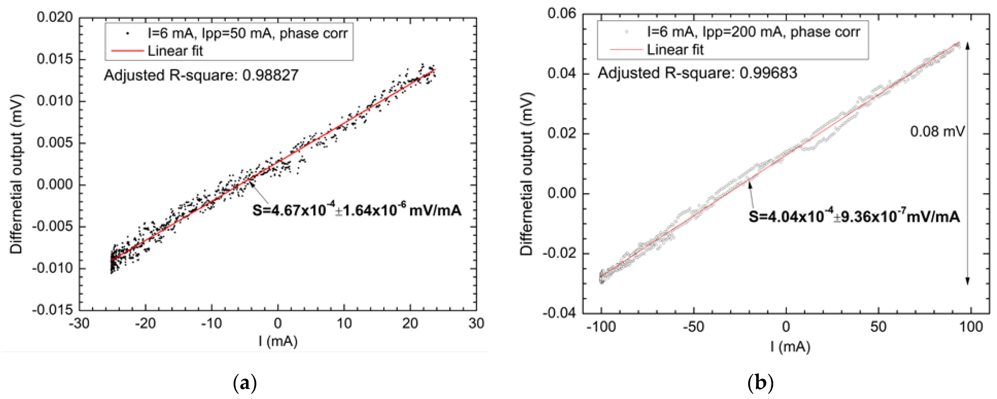
The output voltages from the two sensors were applied to the LabJack EI1040 conditioning system [42], Figure 11, which supplies two voltages at the output, equal with the input voltages but ground referenced. The obtained signal is applied to the K2182A nanovoltmeter. The current through the Ag band is generated by the K6221 source set to generate a sine waveform with 0.04 Hz (thus, quasi-stationary regime). The band current passes through the ground through a R = 6.903 Ω load resistance. The output from this resistor is read by a data acquisition system such that Vdiff = Vsensor1Vsensor2 = f(I) data are acquired. Figure 22 shows the response characteristic of the sensor in differential configuration in function of the current through the printed Ag band. We can note a good linearity of the system with a sensitivity between 4–4.67·10−4 mV/mA. Additionally, from Figure 20b, we can note that the experimental results are in good qualitative agreement with the output signal estimated in Section 3.1.
The demonstrator chip was tested in AC conditions. The total current through the sensors remained 6 mA. The K6221 source was programmed to generate alternative current through the U-shaped trace, Figure 11. The signal was amplified by the SR 560 low noise voltage amplifier from Standford Research; the gain was set to 2·104 and filters were used that cut frequencies higher than 1 kHz and lower than 5 Hz. The signal from the load resistor R = 6.903 Ω is applied on channel 1 and the one corresponding to the current sensor is applied on channel 2 of the HDO 4000 Lecroy Teledyne digital oscilloscope, which allows the analysis of the signal supplied by the chip.
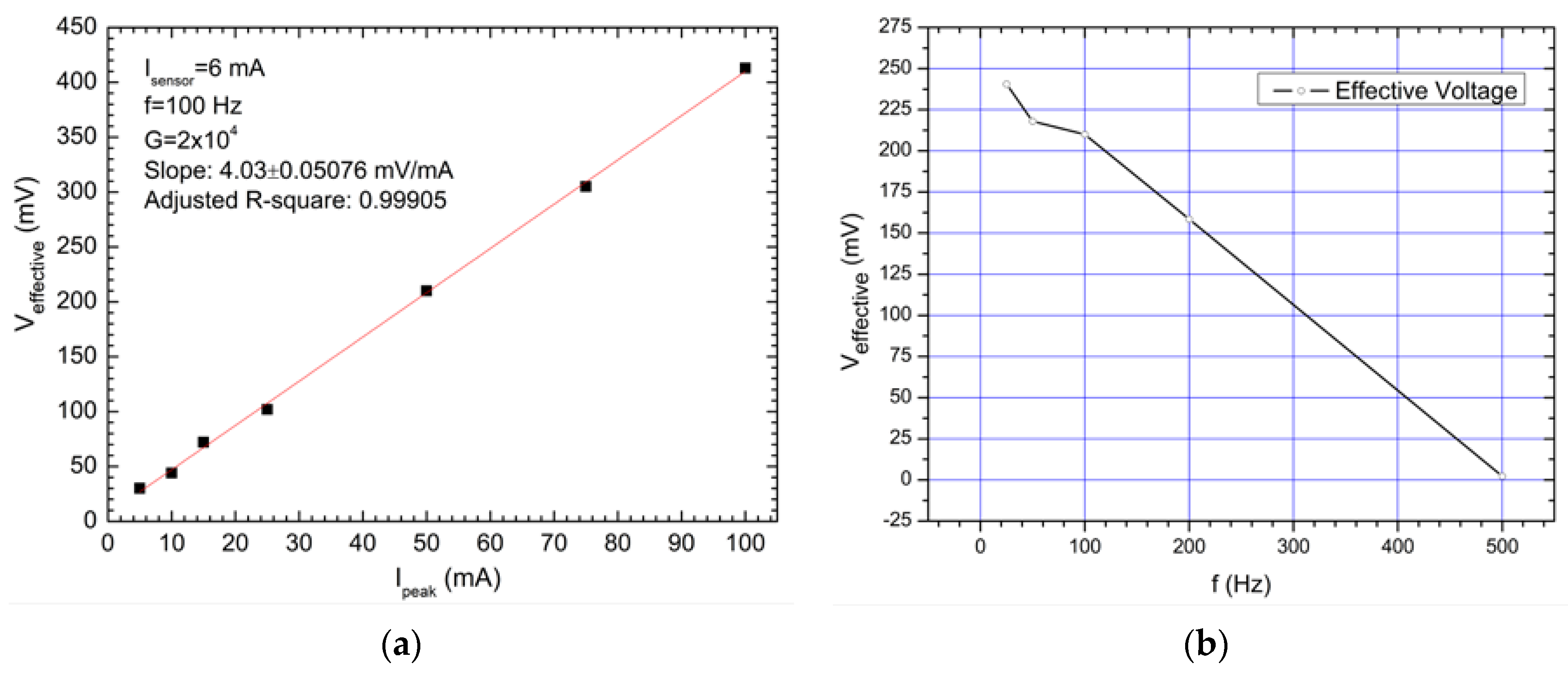
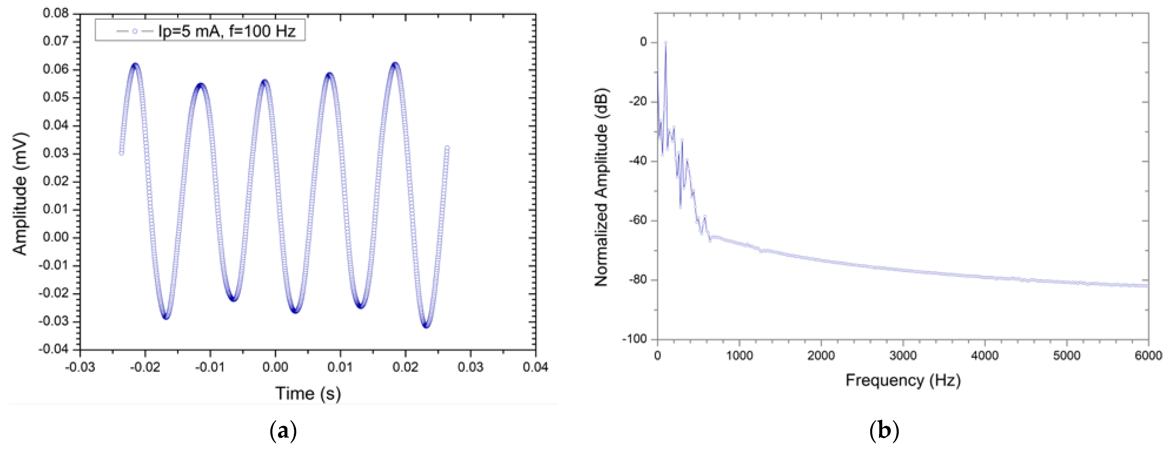
In the Ag band, the current was injected with the following amplitudes: 5, 10, 15, 25, 25, 50, 75 și 100 mA at a 100 Hz frequency. With the HDO 4000 digital oscilloscope, the waveforms of the signal generated by the chip and the effective signal value were measured. The calibration curve was obtained (Figure 23a). Additionally, the frequency response of the sensor was tested in this case, Figure 23b. Finally, in Figure 24, the waveforms obtained for a sinewave current with the amplitude Ipeak = 5, 25, and 50 mA at 100 Hz are shown. From Figure 24, it can be noted that for Ipeak > 15 mA, the waveform of the output voltage shows minimal distortions, following closely the sinusoidal waveform of the current, also confirmed by the Fourier analysis.
The detection limit of the setup is around 2 mA (both DC and AC). The linearity error was determined from Figure 22b by determining a 0.006 mV error for a signal variation of 0.078 mV, which constitutes around a 7.5% linearity error. The sensor was tested between a range of 0–100 mA to avoid any significant thermal effects on the conductive band which can influence the signal stability. Note that the setup aims to serve as a proof of concept and cannot be compared directly with commercial solutions but is now subject to new developments, especially concerning the multilayer structure used to deposit the sensors.

4. Conclusions

The aim of this study is to serve as a basis in designing and optimizing a magnetoresistive bridge sensor for current measurement and low magnetic field sensing. Focus was placed on improving the geometric selectivity of the setup by employing an analytical model which can be used to optimize sensor placement and configuration to achieve the best ratio in terms of sensitivity, complexity, and physical size. The optimization process means: appropriate biasing of the sensor, adequate spacing of components to avoid parasitic magnetic fields, thus greatly improving the sensitivity of the sensor by increasing the useful magnetic field present in the sensor area. This can be applied, for example, for non-destructive testing of electronic circuits when measuring the current in different regions of a printed circuit board.
The magnetic field modeling study of conductive traces for sensing applications has shown that the implemented analytical method can serve as an essential tool for designing high-sensitivity magnetoresistive sensor applications.
The analytical method included four study cases: neglecting the thickness of the trace, dividing the thickness of the trace in several layers, finite or very long conductive trace, and several adjacent traces in the sensor area. It was established that, in terms of accuracy with experimental data, the case of the analytical model when the trace is finite in length and the thickness of the trace is taken into account and divided in an appropriate number of layers, is the most accurate. However, for longer trace lengths, models which neglect the length of the trace can prove more accurate and are closer to the COMSOL FEM model.
A detailed overview of the layout, behavior, and fabrication steps for a demonstrator AMR bridge sensor setup focused on low fields was performed. The behavior of the magnetoresistive structure that comprise the sensor was demonstrated through both equations from a single domain micromagnetic model and simulations using a multi-domain micromagnetic approach. Through micromagnetic simulations, it was proved that only the AMR bridge sensor generates the output depending on the applied field. Other parts of the structure (such as the contacting pads or connecting traces) do not influence the magnetization dynamics of the bridge with the proposed setup.
Very useful data were obtained, such as the optimal number of traces in a planar coil setup to increase the field in the sensor area or the field distribution, depending on the distance from the trace. This method was proven to be accurate when compared with COMSOL simulations and experimental measurements for the implemented AMR bridge sensor and for a giant magnetoresistive (GMR)-based current sensor. Several specific optimizations were performed to the model, which reduce complexity significantly and do not require computationally intensive FEM simulations compared with other solutions shown in the literature [31,33,34,35], which either lack automation or require computationally intense steps. Further developments of the analytical method can focus on geometric corrections for multi-trace or non-linear trace configurations.
Furthermore, the proposed setup aims to create a highly versatile and sensitive sensor setup by taking advantage of inherent benefits in terms of sensor treatment and design (exchange bias field, geometry) and setup advantages (differential configuration, optimized U-shaped trace design, sensors placed in a magnetically shielded box). Given the relatively simple fabrication steps and procedure for the AMR bridge sensor, the proposed sensor design is for proof-of concept purposes only. This approach has some advantages, such as: simple fabrication, reduced costs, ease of use, and integration possibilities and disadvantages, such as: nonlinearity, increased resistivity, and limited sensitivity compared to commercial solutions [43,44,45]. Thus, the novelty of our approach is focused on modeling-setup optimizations and single mask chip microfabrication.
Results were shown for both thermally and magnetically annealed sensors illustrated into a complex testing device for DC/AC testing. From the analysis of the experimental results, a detection limit of approximately ± 2 mA can be estimated. An almost linear characteristic was obtained in the 0–200 Hz range, with an estimated 7.5% linearity error. Results can be significantly improved by utilizing more complex structures based on the GMR or TMR effect, with cross-axis anisotropy, which can lead to significantly enhanced performance of this type of sensor. The findings from this study can also be applied for magnetic nanoparticles detection placed on branches of the PHR sensor instead of the U-shaped stripe. They can be seen as additional sources of the magnetic field which can unbalance the bridge. Future studies can also focus on more complex sensor layouts together with refined analytical modeling in xyz directions and simulations for more complex sensor layouts in multiple axis orientations.

Author Contributions

Conceptualization, C.M., J.N. and M.V.; methodology, C.M, M.V. and M.O.; software, M.O. and M.V.; validation, M.V. and E.H.; formal analysis, M.O.; investigation, C.M. and M.O.; resources, M.V. and J.N.; data curation, E.H.; writing—original draft preparation, C.M.; writing—review and editing, C.M., M.V. and E.H.; visualization, C.M. and M.V.; supervision, M.V. and E.H.; project administration, M.V. and M.V.; funding acquisition, M.V. and J.N. All authors have read and agreed to the published version of the manuscript.

Funding

This research was funded for C.M., M.O., M.V by a grant of the Romanian Ministry of Education and Research, CCCDI-UEFISCDI, project number PN-III-P2-2.1-PED-2019-3514, 510PED/2020, within PNCDI III.

Data Availability Statement

Not applicable.

Conflicts of Interest

The authors declare no conflict of interest.

References

  1. Patel, A.; Ferdowsi, M. Current Sensing for Automotive Electronics—A Survey. IEEE Trans. Veh. Technol. 2009, 58, 4108–4119. [Google Scholar] [CrossRef]
  2. Ripka, P.; Mlejnek, P.; Hejda, P.; Chirtsov, A.; Vyhnánek, J. Rectangular Array Electric Current Transducer with Integrated Fluxgate Sensors. Sensors 2019, 19, 4964. [Google Scholar] [CrossRef] [PubMed] [Green Version]
  3. Snoeij, M.F.; Schaffer, V.; Udayashankar, S.; Ivanov, M.V. Integrated Fluxgate Magnetometer for Use in Isolated Current Sensing. IEEE J. Solid-State Circuits 2016, 51, 1684–1694. [Google Scholar] [CrossRef]
  4. Weiss, R.; Mattheis, R.; Reiss, G. Advanced giant magnetoresistance technology for measurement applications. Meas. Sci. Technol. 2013, 24, 082001. [Google Scholar] [CrossRef]
  5. Nhalil, H.; Givon, T.; Das, P.T.; Hasidim, N.; Mor, V.; Schultz, M.; Grosz, A.; Amrusi, S.; Klein, L. Planar Hall effect magnetometer with 5 pT resolution. IEEE Sens. Lett. 2019, 3, 1–4. [Google Scholar] [CrossRef]
  6. Hung, T.Q.; Oh, S.; Sinha, B.; Jeong, J.R.; Kim, D.Y.; Kim, C. High field-sensitivity planar Hall sensor based on NiFe/Cu/IrMn trilayer structure. J. Appl. Phys. 2010, 107, 9. [Google Scholar] [CrossRef]
  7. Granell, P.N.; Wang, G.; Cañon Bermudez, G.S.; Kosub, T.; Golmar, F.; Steren, L.; Makarov, D.; Fassbender, J. Highly compliant planar Hall effect sensor with sub 200 nT sensitivity. npj Flex. Electron 2019, 3, 10–1038. [Google Scholar] [CrossRef] [Green Version]
  8. Du, W.Y. Resistive, Capacitive, Inductive and Magnetic Sensor Technologies; CRC Press: Boca Raton, FL, USA, 2014; pp. 239–253. [Google Scholar]
  9. Poon, T.Y.; Tse, N.C.F.; Lau, R.W.H. Extending the GMR Current Measurement Range with a Counteracting Magnetic Field. Sensors 2013, 13, 8042–8059. [Google Scholar] [CrossRef] [Green Version]
  10. Soliman, E.; Hofmann, K.; Reeg, H.; Schwickert, M. Noise study of open-loop direct current-current transformer using magneto-resistance sensors. In Proceedings of the 2016 IEEE Sensors Applications Symposium (SAS), Catania, Italy, 20–22 April 2016; IEEE: Piscataway, NJ, USA, 2016; pp. 1–5. [Google Scholar] [CrossRef]
  11. Li, Z.; Dixon, S. A Closed-Loop Operation to Improve GMR Sensor Accuracy. IEEE Sens. J. 2016, 16, 6003–6007. [Google Scholar] [CrossRef]
  12. Ziegler, S.; Woodward, R.C.; Iu, H.H.C.; Borle, L.J. Current sensing techniques: A review. IEEE Sens. J. 2009, 9, 354–376. [Google Scholar] [CrossRef]
  13. Vidal, E.G.; Muñoz, D.R.; Arias, S.I.R.; Moreno, J.S.; Cardoso, S.; Ferreira, R.; Freitas, P. Electronic Energy Meter Based on a Tunnel Magnetoresistive Effect (TMR) Current Sensor. Materials 2017, 10, 1134. [Google Scholar] [CrossRef] [Green Version]
  14. Mușuroi, C.; Oproiu, M.; Volmer, M.; Firastrau, I. High Sensitivity Differential Giant Magnetoresistance (GMR) Based Sensor for Non-Contacting DC/AC Current Measurement. Sensors 2020, 20, 323. [Google Scholar] [CrossRef] [PubMed] [Green Version]
  15. Mușuroi, C.; Oproiu, M.; Volmer, M.; Neamtu, J.; Avram, M.; Helerea, E. Low Field Optimization of a Non-Contacting High-Sensitivity GMR-Based DC/AC Current Sensor. Sensors 2021, 21, 2564. [Google Scholar] [CrossRef] [PubMed]
  16. Ripka, P. Contactless measurement of electric current using magnetic sensors. Tm-Tech. Messen 2019, 86, 586–598. [Google Scholar] [CrossRef] [Green Version]
  17. Volmer, M.; Neamtu, J. Micromagnetic analysis and development of high sensitivity spin-valve magnetic sensors. J. Phys. Conf. Ser. 2011, 268, 012032. [Google Scholar] [CrossRef]
  18. Sreevidya, P.V.; Khan, J.; Barshilia, H.C.; Ananda, C.M.; Chowdhury, P. Development of two axes magnetometer for navigation applications. J. Magn. Magn. Mater. 2018, 448, 298–302. [Google Scholar] [CrossRef]
  19. Hauser, H.; Tondra, M. Magnetoresistors. In Magnetic Sensors and Magnetometers; Ripka, P., Ed.; Artech house: Norwood, MA, USA, 2001; pp. 136–144. [Google Scholar]
  20. Hansen, M.F.; Rizzi, G. Exchange-biased AMR bridges for magnetic field sensing and biosensing. IEEE Trans. Magn. 2016, 53, 1–11. [Google Scholar] [CrossRef] [Green Version]
  21. Henriksen, A.D.; Dalslet, B.T.; Skieller, D.H.; Lee, K.H.; Okkels, F.; Hansen, M.F. Planar Hall effect bridge magnetic field sensors. Appl. Phys. Lett. 2010, 97, 013507. [Google Scholar] [CrossRef]
  22. Elzwawy, A.; Pişkin, H.; Akdoğan, N.; Volmer, M.; Reiss, G.; Marnitz, L.; Schmalhorst, J.M.; Moskaltsova, A.; Gurel, O. Current trends in planar Hall effect sensors: Evolution, optimization, and applications. J. Phys. D Appl. Phys. 2021, 54, 353002. [Google Scholar] [CrossRef]
  23. McGuire, T.; Potter, R.L. Anisotropic magnetoresistance in ferromagnetic 3d alloys. IEEE Trans. Magn. 1975, 11, 1018–1038. [Google Scholar] [CrossRef]
  24. Lin, G.; Makarov, D.; Schmidt, O.G. Magnetic sensing platform technologies for biomedical applications. Lab A Chip 2017, 17, 1884–1912. [Google Scholar] [CrossRef] [PubMed]
  25. West, F.G. Rotating-field technique for galvanomagnetic measurements. J. Appl. Phys. 1963, 34, 1171–1173. [Google Scholar] [CrossRef]
  26. Tumanski, S. Thin film Magnetoresistance Sensors; CRC Press: Boca Raton, FL, USA, 2001. [Google Scholar]
  27. Jogschies, L.; Klaas, D.; Kruppe, R.; Rittinger, J.; Taptimthong, P.; Wienecke, A.; Wurz, M.C.; Rissing, L. Recent developments of magnetoresistive sensors for industrial applications. Sensors 2015, 15, 28665–28689. [Google Scholar] [CrossRef] [PubMed] [Green Version]
  28. Hauser, H.; Stangl, G.; Fallmann, W.; Chabicovsky, R.; Riedling, K. Magnetoresistive Sensors, Preparation, Properties, and Applications of Thin Ferromagnetic Films, June 2000. Available online: http://educypedia.karadimov.info/library/Hauser.pdf (accessed on 23 November 2022).
  29. Jander, A.; Smith, C.; Schneider, R. Magnetoresistive sensors for nondestructive evaluation. Adv. Sens. Technol. Nondestruct. Eval. Struct. Health Monit. 2005, 5770, 1–13. [Google Scholar] [CrossRef]
  30. NVE Sensors Catalogue. Available online: https://www.nve.com/Downloads/catalog.pdf (accessed on 23 November 2022).
  31. Misakian, M. Equations for the magnetic field produced by one or more rectangular loops of wire in the same plane. J. Res. Natl. Inst. Stand. Technol. 2000, 105, 557. [Google Scholar] [CrossRef]
  32. Nicolaide, A. Electromagnetics. General Theory of the Electromagnetic Field. Classical and Relativistic Approaches, 3rd ed.; Transilvania University Press: Brașov, Romania, 2012; pp. 170–173. [Google Scholar]
  33. Minnaert, B.; Stevens, N. Evaluation of The Vertical Magnetic Field Generated By A Spiral Planar Coil. In Proceedings of the Nordic Circuits and Systems Conference (NORCAS), Oslo, Norway, 26−28 October 2015; NORCHIP & International Sympo-sium on System-on-Chip (SoC). pp. 1–3. [Google Scholar] [CrossRef]
  34. Hrabovský, P.; Kravets, O. The Design and Simulation of Spiral Planar Coil in COMSOL Multiphysics. In IEEE International Conference on Modern Electrical and Energy Systems (MEES); IEEE: Piscataway, NJ, USA, 2019; pp. 374–377. [Google Scholar] [CrossRef]
  35. Gupta, M.; Agarwal, P. To model magnetic field of RF planar coil for portable NMR applications. In Proceedings of the In-ternational Conference on Inventive Computing and Informatics (ICICI), Coimbatore, India, 23−24 November 2017; pp. 490–494. [Google Scholar] [CrossRef]
  36. NVE ALTxxx-10 TMR Catalogue. Available online: https://www.nve.com/Downloads/ALTxxx-10.pdf (accessed on 23 November 2022).
  37. Voltera V-One Printer Overview. Available online: https://f.hubspotusercontent30.net/hubfs/5264434/Sales-Docs/Product-Development.pdf (accessed on 23 November 2022).
  38. Leliaert, J.; Mulkers, J. Tomorrow’s micromagnetic simulations. J. Appl. Phys. 2019, 125, 180901. [Google Scholar] [CrossRef]
  39. Yin, L.F.; Wei, D.H.; Lei, N.; Zhou, L.H.; Tian, C.S.; Dong, G.S.; Jin, X.F.; Guo, L.P.; Jia, Q.J.; Wu, R.Q. Magnetocrystalline anisotropy in permalloy revisited. Phys. Rev. Lett. 2006, 97, 067203. [Google Scholar] [CrossRef] [Green Version]
  40. Roshchupkina, O.D.; Strache, T.; McCord, J.; Mücklich, A.; Bähtz, C.; Grenzer, J. Structural modifications of thin magnetic Permalloy films induced by ion implantation and thermal annealing: A comparison. Acta Mater. 2014, 74, 278–284. [Google Scholar] [CrossRef]
  41. Voltera Flexible Conductor Ink Datasheet. Available online: https://assets.ctfassets.net/e6vf9wdhbae5/2z1lTqP8uRIxYLRCSZ9hCQ/839deb49846f3e75878cea856297f7eb/Voltera-Flexible-Conductive-Ink.pdf (accessed on 23 November 2022).
  42. LabJack EI1040 Instrumentation Amplifier. Available online: https://labjack.com/products/ei1040-dual-instrumentation-amplifier (accessed on 23 November 2022).
  43. Mlejnek, P.; Vopalensky, M.; Ripka, P. AMR current measurement device. Sens. Actuators A 2008, 141, 649–653. [Google Scholar] [CrossRef]
  44. Aceinna Current Sensors Catalogue. Available online: https://www.aceinna.com/current-sensors (accessed on 23 November 2022).
  45. Sensitec Current Sensors Catalogue. Available online: https://www.sensitec.com/products-solutions/current-measurement/cfs1000 (accessed on 23 November 2022).
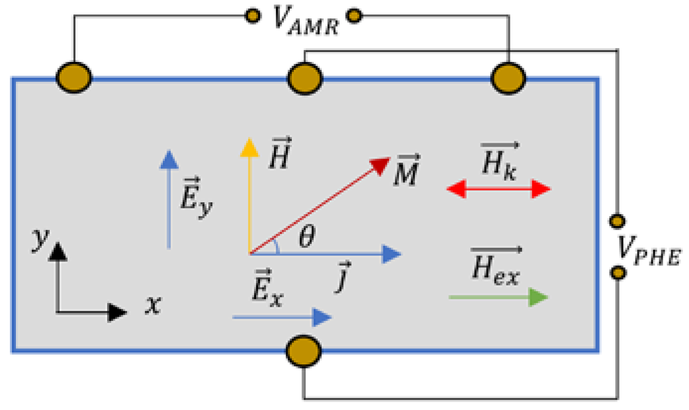
Figure 1. Schematic representation of the AMR and PHE effects on a Permalloy thin film through which a current is flowing along the x axis; M is the magnetization which makes an angle θ with the current direction due to the applied field, H which is perpendicular on the applied current.
Electronics 11 03888 g001
Figure 2. Working principle of the non-contacting current measurement setup utilizing current traces and a MR-based chip: (a) Single trace plane section; (b) Multi-trace plane section; (c) Single trace cross section; (d) Multi-trace cross section (adapted from [15]).
Electronics 11 03888 g002
Figure 3. Analytical model to compute the magnetic field present in the sensor area: (a) Length correction of the magnetic field in the sensor area based on the distance from the linear trace ends; (b) Magnetic field components generated by the current through the trace and dimensional parameters; (c) Layered trace thickness parameters. Note that the model takes into account that there is an odd number of traces that generate the magnetic field and the central trace is denoted as n = 0.
Electronics 11 03888 g003
Figure 4. Design and experimental implementation of (a) Geometry and parameters for the U-shaped trace; (b) Plane view of the planar coil with seven traces.
Electronics 11 03888 g004
Figure 5. Layout of the exchange biased AMR bridge sensor chip: (a) Chip layout with over imposed U-shaped current trace on top of the AMR bridges; (b) Dimensions of the chip; (c) Working principle of the AMR bridge sensor; (d) Equivalent circuit of a single AMR bridge sensor. Note that the structured is within a square of 4 × 4 mm2 and was realized on a 5 × 5 mm2 chip. The margins are 0.5 mm while the arm of the bridge has a length L = 1 mm and a width of either 0.1 or 0.2 mm. The contacting pads size can be reduced such that the chip can fit inside a 3 × 3 mm2 footprint.
Electronics 11 03888 g005
Figure 6. AMR bridge sensor, multi-domain simulation mask layout: (a) SEM image of the sensor with obtained mask image after editing; (b) Overview of the imported mask in the software with the marked direction of the applied field and exchange bias field.
Electronics 11 03888 g006
Figure 7. Simulated multi-domain magnetization distribution of the AMR bridge structure at different field values (H = 0 Oe, H = −150 Oe, H = 150 Oe, H = 250 Oe). The red arrow signifies the direction of the applied field while the blue arrow shows the orientation of the exchange bias field. The encircled areas show that no matter the field value, the orientation of the magnetic moments does not change and does not influence the behavior of the central area of the structure, thus there is no signal change with the applied field for these areas.
Electronics 11 03888 g007
Figure 8. AMR bridge sensor, multi-domain simulation results for low field values: (a) Magnetization distribution along the x-axis; (b) Magnetization distribution along the y-axis; (c) PHE signal for the entire structure; (d) PHE signal for the central area of the structure (bridge).
Electronics 11 03888 g008
Figure 9. (a) SEM image of the AMR bridge sensor; (b) Direction and intensity of the applied field, B over the structure during the magnetic annealing process.
Electronics 11 03888 g009
Figure 10. Voltera V-One printer with printed U-shaped traces and printed traces detail.
Electronics 11 03888 g010
Figure 11. Functional block diagram of the experimental setup for the AMR bridge sensor demonstrator chip.
Electronics 11 03888 g011
Figure 12. Measurement schematic for the AMR bridge sensors: (a) For the thermally annealed chip; (b) For the thermally and magnetically annealed chip.
Electronics 11 03888 g012
Figure 13. Demonstrator setup: (a) Steps for assembling the demonstrator chip; (b) The sensor mounted in the shielded box, as implemented for characterization and testing.
Electronics 11 03888 g013
Figure 14. Thermally annealed AMR bridge sensor, field characteristics: (a) No applied biasing field; (b) Field characteristics for different Hbias values.
Electronics 11 03888 g014
Figure 15. Thermally and magnetically cured AMR bridge sensor, field characteristics at different biasing levels (Hbias = 0, 45, 80 Oe): (a) Field characteristics for sensor 1; (b) Field characteristics for sensor 2 Hbias = 80 Oe bias level.
Electronics 11 03888 g015
Figure 16. Helmholtz coil supply current-field dependency, H(I) characteristic in the sensor area.
Electronics 11 03888 g016
Figure 17. Magnetic field distribution on the x-axis for the U-shaped trace and planar coil for a 100 mA current according to COMSOL simulations: (a) U-shaped current trace: Hx field distribution at height h = 45 µm ( H x _ s e n s o r = 40.630   A / m ) and h = 80 µm ( H x _ s e n s o r = 39.056   A / m ) from the current trace; (b) Multitrace (7 traces): Hx field distribution at height h = 45 µm ( H x _ s e n s o r = 126.67   A / m ) and h = 80 µm ( H x _ s e n s o r = 121.94   A / m ) from the current trace.
Electronics 11 03888 g017
Figure 18. Magnetic field intensity on the x direction, variation for the U-shaped trace at height h = 45 µm according to results from COMSOL simulation: (a) transverse center line (note the inset); (b) longitudinal center line (note the inset).
Electronics 11 03888 g018
Figure 19. Magnetic field intensity on the x direction, variation for the Multitrace planar coil with 7 traces at height h = 80 µm from the trace according to results from COMSOL simulation: transverse center line (note the inset).
Electronics 11 03888 g019
Figure 20. (a) Magnetic field intensity Hx, variation for different h (0.08 mm to 2.08 mm) for the “U-shaped current trace according to results from COMSOL simulation and from the analytical model; (b) Magnetic field intensity Hx, variation for different h (0.08 mm to 3.58 mm) for the “Planar coil with 7 traces” according to results from COMSOL simulation and from the analytical model; The current through the trace was 100 mA.
Electronics 11 03888 g020
Figure 21. Magnetic field intensity obtained according to the analytical method in the sensor area, dependency on the number of traces in the case of a planar coil (the same parameters as for the 7 traces planar coil were used in this case). Note that m = 35 layers (1 μm each layer).
Electronics 11 03888 g021
Figure 22. Response characteristics of the differential sensor, depending on the value of the current through the printed Ag trace for: (a) Low currents up to 25 mA; (b) Currents up to 100 mA.
Electronics 11 03888 g022
Figure 23. (a) AC calibration curve in the 0–100 mA range for a 100 Hz sinewave; (b) Frequency response of the output voltage for a 50 mA amplitude (peak-to-peak) sinewave.
Electronics 11 03888 g023
Figure 24. Demonstrator chip: Time-domain characteristics (a,c,e) and Fourier transforms (b,d,f) for the output voltage when a 5 mA, 100 Hz, sinusoidal waveform current is injected into the U-shaped trace, f = 100 Hz, with the amplitude of: (a,b) 5 mA; (c,d) 25 mA; (e,f) 50 mA.
Electronics 11 03888 g024aElectronics 11 03888 g024b
Table 1. Parameters utilized for the analytical model and COMSOL simulation (U-shaped trace and planar coil).
SymbolNameQuantity
DTrace widthPlanar coil with 7 traces: 0.22 mm
U-shaped trace: 1.2 mm
TdDistance between tracesPlanar coil with 7 traces: 0.19 mm
U-shaped trace: N/A
ICurrent through trace0.1 A
hDistance between
sensor
and trace
Planar coil with 7 traces: 0.045 [mm] to
3.58 [mm]
U-shaped trace: 0.045 mm to 2.08 mm
tTrace thickness35 µm
mNumber of layers in
which t is divided
35 (1 μm each layer)
LTrace lengthPlanar coil with 7 traces: 42 mm
U-shaped trace: 3.2 mm
ΔlSensor position on
trace length 1
Planar coil with 7 traces: 21 mm
U-shaped trace: 1.6 mm
VsSensor input voltage U-shaped trace setup: 4.399 V
Planar coil setup: 4.096 V
SSensor sensitivity U-shaped
trace sensor setup:
S1: 159 μV/(V × A/m)
(0.01268 mV/V-Oe)
S2: 188.54 μV/(V × A/m) (0.0150034 mV/V-Oe)
Sdifferential: 347.94 μV/(V × A/m) (0.0277 mV/V-Oe)
Planar coil
sensor setup:
Sdifferential: 32.67 μV/(V × A/m)
1 The sensor position on the trace length is given by Δ l L · 100   % .
Table 2. Comparative analysis between COMSOL simulation, analytical model, and experimental data.
Trace TypeValidation Caseh 1
[mm]
Hx
[A/m]
Vout2
[mV]
Vdifferential 2
[mV]
U-shaped trace
(Figure 4a)
Itrace = 100 mA
Vs = 4.399 V 3
COMSOL simulations0.0839.056--
0.04540.630--
Analytical
method
Case I: Infinite length,
t neglected
0.0838.150S1: 0.026750.05839
S2: 0.03164
0.04539.680S1: 0.027820.06073
S2: 0.03291
Case II: Infinite length, m = 35 layers
(1 μm each layer)
0.0836.7321S1: 0.025750.05622
S2: 0.03046
0.04538.2408S1: 0.026810.05853
S2: 0.03171
Case III: Finite length,
t neglected
0.0832.0769S1: 0.022490.04910
S2: 0.0266
0.04533.3818S1: 0.023410.05109
S2: 0.02768
Case IV: Finite length, m = 35 layers
(1 μm each layer)
0.0830.8842S1: 0.021650.04727
S2: 0.02561
0.04532.1704S1: 0.022550.04924
S2: 0.02668
Experimental results0.04531.7423S1: 0.0198 0.042
S2: 0.022
Planar coil with
7 traces
(Figure 4b)
Itrace = 100 mA
Vs = 4.096 V 3
COMSOL simulation0.879.780--
0.08121.94--
Analytical
method
Case I: Infinite length,
t neglected
0.882.588511.870223.7404
0.08157.42222.625745.2514
Case II: Infinite length, m = 35 layers
(1 μm each layer)
0.881.242811.676823.3536
0.08140.62420.211540.423
Case III: Finite length,
t neglected
0.867.94989.983819.9676
0.08132.46519.038838.0776
Case IV: Finite length, m = 35 layers
(1 μm each layer)
0.866.84279.82119.642
0.08118.33117.007334.0146
Experimental results 0.8-10.716 21.432
1 Distance between the sensing element and the current trace. Note that 0.045 mm is the distance between the sensors and the U-shaped trace in the experimental setup and 0.8 mm is the distance between the sensing element and the current trace in the experimental setup for the planar coil with the AA003-02 encapsulated sensors [31]. 2 Output voltage for a single sensor (Vout) and for the two sensors in differential configuration (Vdifferential). 3 Sensors supply voltage in differential configuration.
Publisher’s Note: MDPI stays neutral with regard to jurisdictional claims in published maps and institutional affiliations.