Article

Soft Error Sensitivity Analysis Based on 40 nm SRAM-Based FPGA

1
School of Nuclear Science and Technology, University of South China, Hengyang 421001, China
2
Science and Technology on Reactor System Design Technology Laboratory, Nuclear Power Institute of China, Chengdu 610213, China
*
Author to whom correspondence should be addressed.
Electronics 2022, 11(23), 3844; https://doi.org/10.3390/electronics11233844
Submission received: 29 October 2022 / Revised: 16 November 2022 / Accepted: 18 November 2022 / Published: 22 November 2022
(This article belongs to the Section Circuit and Signal Processing)

Abstract

:
Soft errors induced by radiation are the major reliability threat for SRAM-based field-programmable gate arrays (FPGAs). A more detailed analysis of the soft error sensitivity of the 40 nm SRAM-based FPGA was performed. Experimental methods for the configurable logic module, configure memory cells, and block RAM have been introduced for measuring the single event effects (SEEs) induced by alpha particles using a 241Am radiation source. The single event upset (SEU) and single event functional interrupt (SEFI) cross sections of different functional blocks have been calculated to discuss the failure mechanisms of the FPGA. The SEEs test results for the FPGA device based on the 40 nm CMOS process are significant.

1. Introduction

Because of its configuration flexibility, great computational power, low power consumption and other useful features, the SRAM-based FPGA is widely used in industrial, safety-critical, nuclear and aerospace application fields. In particular, the FPGA is very attractive to the aerospace sector because it helps with system integration, control optimization and miniaturization. A range of FPGA products have been successfully applied to satellites, controllers, data processors and deep space detectors [1,2,3,4]. However, electronic devices are susceptible to radiation environments, especially single event effects (SEEs). Therefore, SEEs induced by radiation particles are a serious threat to the reliability of SRAM-based FPGAs.
SEEs are the result of the interaction of highly ionized particles, such as heavy ions, alpha particles and neutrons, with sensitive regions of a microelectronic device. The high number of electron-hole pairs generated by the incident particles are collected by the sensitive junctions of the device, resulting in local transient ionization phenomena that lead to changes in the logic state of the semiconductor device or integrated circuit, parasitic structural circuit conduction, etc. [5,6]. SEE events can be divided into two categories: software errors (recoverable errors) and hardware errors (quasi-permanent and permanent errors) [7,8]. The software errors can be mitigated by resetting or reconfiguring the device so that it returns to its nominal functional state, methods for which include single event upset (SEU), single event transient (SET), and single event function interrupt (SEFI). Moreover, it is one of the major causes for spacecraft anomalies and failures. The hardware errors, such as single event latch-up (SEL), may have serious implications and cause permanent damage to the device if not mitigated in time, while single event burnout (SEB) and single event gate rupture (SEGR) are permanent and destructive errors.
There are three FPGA architectures, namely the SRAM-based FPGA, the flash-based FPGA and the antifuse-based FPGA. Compared with SRAM-based FPGAs, flash-based FPGAs are less densely integrated and more expensive, and antifuse-based FPGAs lack reproducible programming capabilities, although both are slightly more resistant to irradiation [9,10]. SEUs can insert a fault into the configuration memory, block memory and flip-flop to alter the FPGA system functions and cause failure. The SRAM-based FPGA contains a large sum of memory resources, especially configuration memory, so it is the most susceptible to SEUs. Irradiation tests can be performed to characterize the sensitivity of FPGAs and obtain an SEE cross section. A radiation effects experiment is the most effective measure for reflecting the real situation of electronic devices in a radiation environment. The radiation sources for the experiment consist of a particle accelerator, a nuclear reactor, an alpha source and a neutron source.
SEE research of the Xilinx SRAM-based FPGA has been performed with different FPGA types [11,12,13,14,15,16]. Heavy ion, proton and neutron radiation experiments have been carried out to characterize the sensitivity of Xilinx’s SRAM-based FPGA and obtain SEU cross sections of different functional blocks, such as the configuration RAM, block RAM and configuration logic blocks. It is important to investigate the SEEs of different commercial off-the-shelf (COTS) devices to screen out the devices that can best meet the requirements of space application fields. However, SEE research about SRAM-based FPGAs made in China has been undertaken less frequently. In order to promote the application of FPGAs in the aerospace and nuclear radiation fields, a significant effort should be undertaken to push forward independent research on radiation-hardened FPGAs. Because alpha particle content can be up to 14% in a space radiation environment, and since they come from the packaging materials and from the nuclear reaction of neutrons with boron doping in semiconductor devices [17,18], the single event effect of the FPGA based on 40 nm CMOS technology made by the PANGOMICRO company was investigated with a 241Am alpha radiation source in this paper.
In this work, a SRAM-FPGA device based on the 40 nm CMOS process was used as the research object. Firstly, the device under test was introduced to analyze the hardware resources; secondly, the SEE test methods and test system were explained; thirdly, the SEE sensitivity and error type for different functional units of the FPGA were analyzed; finally, the discussion and analysis of the experimental results provide a reference for the radiation hardening of the SEE area module.

2. Device under Test

2.1. Test Board

The FPGA test board is derived from the ALINX company’s development board. It is composed of a PANGO FPGA core board attached to an expansion board. The PGL22G FPGA, 256 MB DDR3 and 128 MB QSPI FLASH are the key components of the FPGA core board. It is responsible for high-speed data processing and the storage function. The FPGA is widely utilized in video image processing, high-speed data collection and communication areas due to its inherent high performance, high speed, high bandwidth and high capacity. The extension board includes several interfaces for the core board to communicate with external devices. It has a 10/100/1000 M ethernet port, a USB 2.0 port, a UART port, a secure digital memory card (SD) interface, a high-density multi-chip interconnect (HDMI) output port, a JTAG, a 4 Kbit EEPORM and 40 Pin I/O expansion interfaces, as illustrated in Figure 1 [19].

2.2. Test Chip

This alpha SEE experiment was carried out using the PGL22G SRAM-FPGA. It is fabricated on a 40 nm copper CMOS process run at a core voltage of 1.1 V. It includes a configurable logic module (CLM), flip-flops, distributed RAM, an 18 Kb dedicated block RAM module (BRAM), an arithmetic process module (APM), a hard ADC, a hard memory controller, a double data rate (DDR), a phase locked loop (PLL), a joint test action group (JTAG) interface, an advanced encryption standard (AES), a high speed signal test (HSST) and various I/O resources, as shown in Table 1. Additional information can be found in the datasheets provided by the manufacturer [19].

2.3. Test Module Analysis

The fault types induced by the SEEs of FPGAs can be divided into two main categories: faults caused by SEUs in the configuration memory, user memory, and flip-flops; and faults caused by SEFIs, which cause program function interruptions or program corruptions.
The configurable logic module (CLM) is the basic logic unit and consists of the multifunctional look-up table (LUT) structure, registers and extended function selectors, which are the primary resources for the implementation of system functions. The LUT is essentially RAM-based and functions similarly to a combinatorial logic function generator. A large number of register cells store information about the configuration of the circuit and the data for the control system. When a SEU error occurs in them, it may quickly lead to faults in the logic functions and subsequent outputs of the circuit. Thus, the sensitivity of this module to SEEs must be evaluated.
Configure memory cells (CRAM) are used to store in SRAM cells configuration data that are implemented through internal programmable modules such as CLM, interconnect resources (IR) and I/O block (IOB), physically distributed throughout the chip. The size of the resource of the configuration memory cell is huge, so if a SEU occurs in the underlying configuration cells such as look-up tables, configurable control bits, switch matrices and programmable interconnects, it can easily lead to errors in user’s logic output. On the other hand, SEUs occurring in the underlying configuration data that are represented by block memories or flip-flops routing, conversely, have no effect on the user’s logic output results and timing circuitry. As a result, errors in the configuration memory’s critical configuration bit can change the circuit structure and thereby cause system logic function corruption until its reconfiguration.
BRAM is a dedicated memory module inside the FPGA that can be freely configured by the user. The occurrence of a single event upset could cause errors in the user data stored in the BRAM, thus affecting the normal operation of the FPGA’s functions. With the FPGA’s arrays continuing to grow in size and its application scenarios diversifying, the storage capacity of BRAM increases exponentially. The BRAM storage bit count on the FPGA chip used in this work is 792 Kbit.

3. SEE Test Methods

According to the SEE sensitivity characteristics of different resources inside SRAM-FPGA devices, the SEE tests for SRAM-FPGA are divided into a configuration memory test, a block memory test and a CLM test with static test and dynamic test methods. The different blocks of the PGL22G FPGA were checked during irradiation. These test methods are described in detail as follows.

3.1. CRAM Test

The configuration memory module was tested using static testing methods. Static testing was performed on the entire device to test the sensitivity of the memory elements in a radiation environment. During the test, the FPGA was built to maximize configuration memory consumption, and the FPGA was made to be in a static condition by masking the external crystal clock signal. When the total cumulative fluence of irradiated particles was more than 1 × 10 7 particles · cm 2 , the data in the configuration memory were read back and compared with the unirradiated data to determine the sensitivity to the SEE.
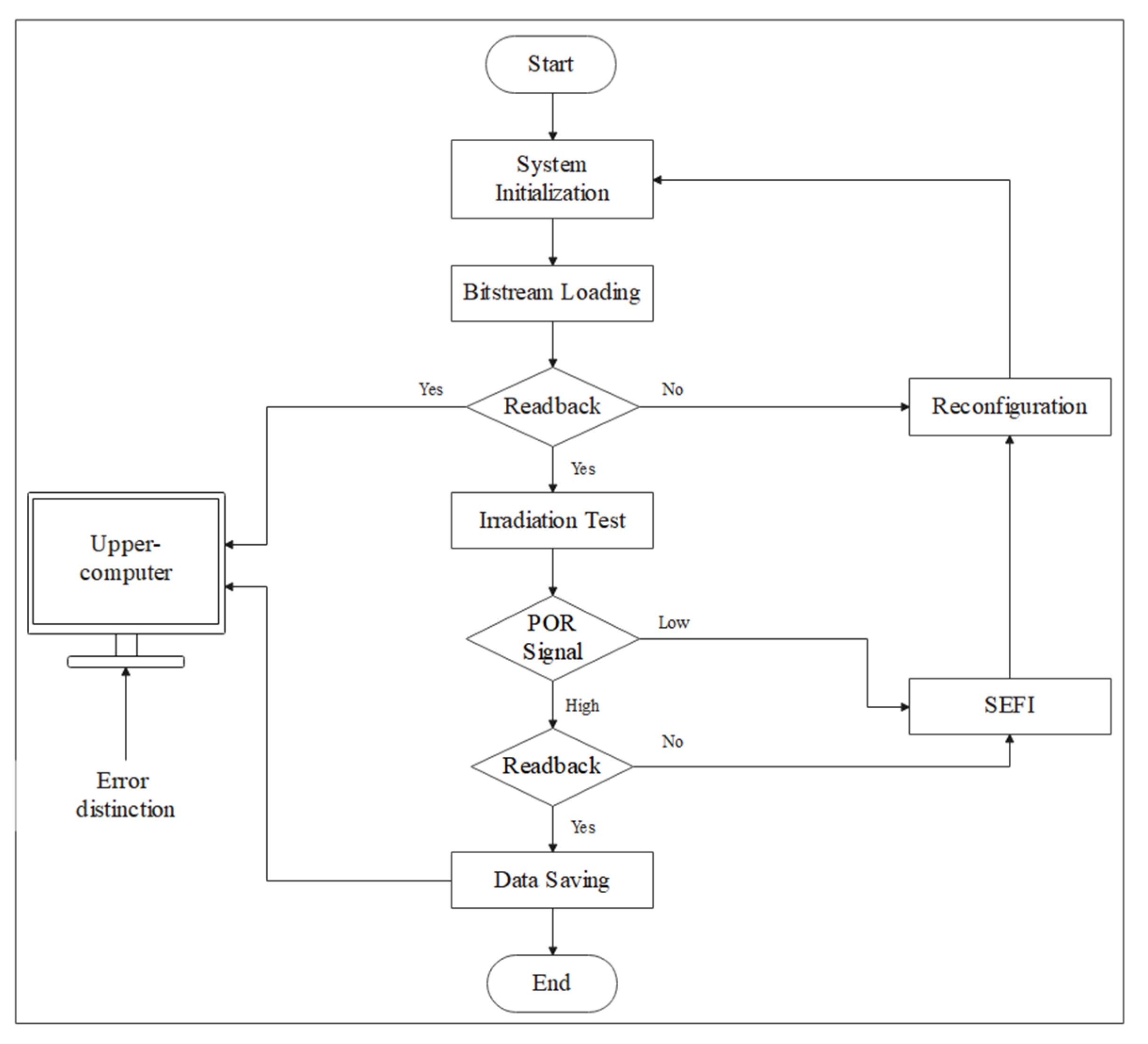
The configuration file (bitstream file), which was created by the EDA tool based on the pre-designed software, was downloaded and read back using the JTAG connection before the irradiation test. The process is shown in Figure 2: First, the DUT was connected to the power supply, the JTAG port and the host PC by a USB cable, which was used to configure and readback the bitstream file and to confirm the successful configuration of the DUT before the irradiation experiment. Second, in order to determine whether a SEFI has occurred in the DUT, the operational condition of the FPGA was monitored during the irradiation test, the configuration data were readback at intervals and the power-on reset (POR) signal light was detected. The POR signal light turning off meant that a SEFI had occurred and the chip needed to be reconfigured. However, if a SEFI didn’t occur when the fluence of alpha particles reached 107 particles·cm−2 magnitudes, the configuration memory data would be readback and generate a mask file. With the help of the mask file, the readback data for pre-irradiation and post-irradiation were compared to determine the number of flipped bits out of a total of 762,528 configuration bits, and then the flipped cross section of the configuration memory was obtained.

3.2. BRAM Test

A dynamic test approach was used in the SEE test of the block RAM [20]. During the irradiation, the operating state of the circuit was monitored in real time. Once a failure occurred in the DUT, it was noted as one functional error, and then the device was reconfigured to ensure the validity of next test.
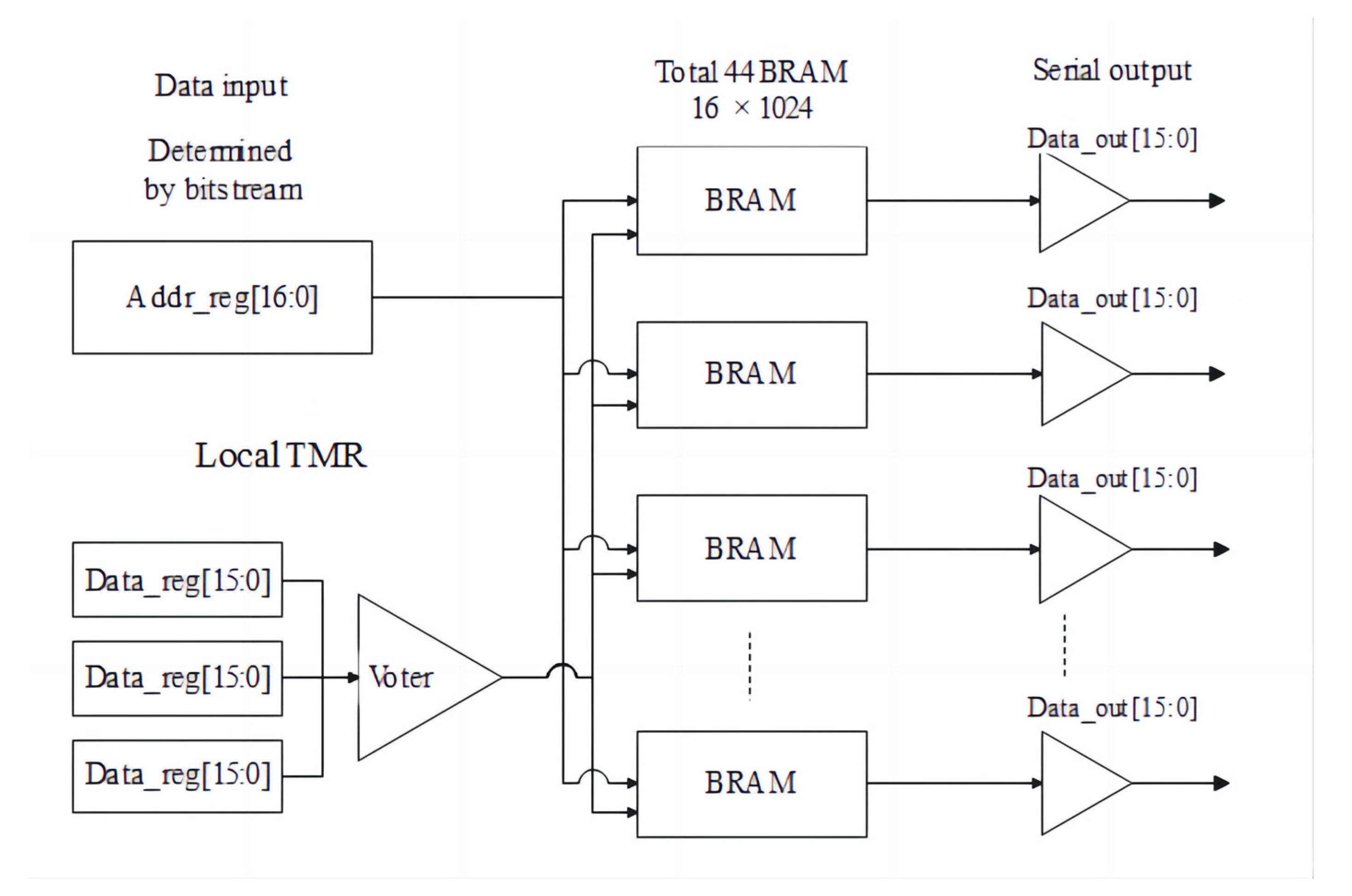
The dedicated BRAM of the PGL22G SRAM-FPGA has up to 18 K bits and can be configured independently as two 8 K bits or one 16 K bits, for a total of 48 BRAM cells. Each BRAM supports DP (True Dual Port) RAM mode and can also be configured for SP (Single Port) RAM mode, SDP (Simple Dual Port) RAM mode, ROM mode, and synchronous/asynchronous FIFO mode [21]. The test circuit was designed to configure the block memory as a synchronous FIFO with a bit-width of 16 and a depth of 1024 (16 × 1024). A total of 44 identical FIFOs were designed to form a FIFO chain in this circuit, as shown in Figure 3, and data 0XFFFF was written to the FIFO chain simultaneously through the data register module that was reinforced with a local triple-mode redundancy scheme to achieve radiation-resistant reinforcement and reduce data errors caused by SEEs in the data registers. The data read from the FIFO chain were then sent to the host computer for storage with the serial ports data transmitter module. During the experiment, the running status of the program needed to be continuously monitored to ensure that the FPGA could be reconfigured in time when a program function interruption took place. The sensitivity of the test module to SEEs was determined by recording the number of interruptions and comparing read and write data. This test method contributes more than 90% of the FPGA’s BRAM resources and can be used to test the SEE sensitivity of the BRAM.

3.3. CLM Test

SEEs of the CLM were investigated by the dynamic test method. Both the LUT cell and the flip-flop cell in the CLM were designed as a shift register chain. All the shift registers were filled with the 0XFFFFFFFF and started to shift at the same clock. To prevent one datum in the shift-registers from being flipped over several times after shifting, which would affect the accuracy of the experimental results, the shifted data were output after each shift of the shift register in the test. The data before and after the shift were compared to ensure whether the data were flipped or not. If they were flipped, they were reset to the initial data, and if they weren’t flipped, the function of shifting would continue. Each CLM was composed of four five-input LUTs (LUT5s) and six registers. In this test, 160 shift registers were used to form a shift register chain, and the shifted data were output by the serial output module, which was compared with the written data, with the number of bits that differed being the number of flipped bits. The SEFI was monitored in the same way as in the BRAM test. This test method allowed a more accurate assessment of the SEE sensitivity of the CLM.

4. SEE Experiments

4.1. Radiation Source

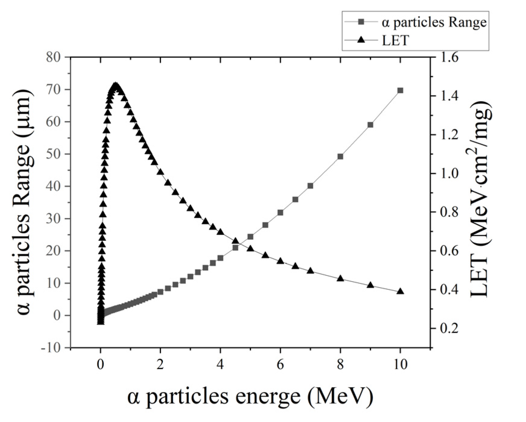
As known from the decay equation for the 241Am source, 237Np was produced mainly with three different energies of alpha particles and a small amount of gamma ray production (e.g., 84.8% of 5.486 MeV alpha particles, 13.1% of 5.443 MeV alpha particles, 1.66% of 5.388 MeV alpha particles and 35.9% of 59.541 keV gamma rays) [22]. For the alpha particles with an energy of 5.486 MeV, the LET value was 0.5758 MeV · cm 2 / mg , which has a range in silicon of about 27.9   μ m , as shown in Figure 4.
The parameters of the radioactive source are listed in Table 2. Alpha particles are emitted isotropically at a rate of 2 π from the surface of a cylindrical source with a thickness of 1 mm and a diameter of 45 mm. It has an emissivity of 1.21 × 10 6   particles / 2 π minute , which is much higher than the alpha particle emissivity in the real environment. All these parametric conditions are in accordance with international standards, i.e., JESD89 A [23], so it is suitable to be used for the accelerated testing of soft error rates introduced by alpha particles. In this experiment, the chip under test must have the packaging material removed from its surface to ensure that the particles are able to reach the sensitive areas inside the chip.

4.2. Test System

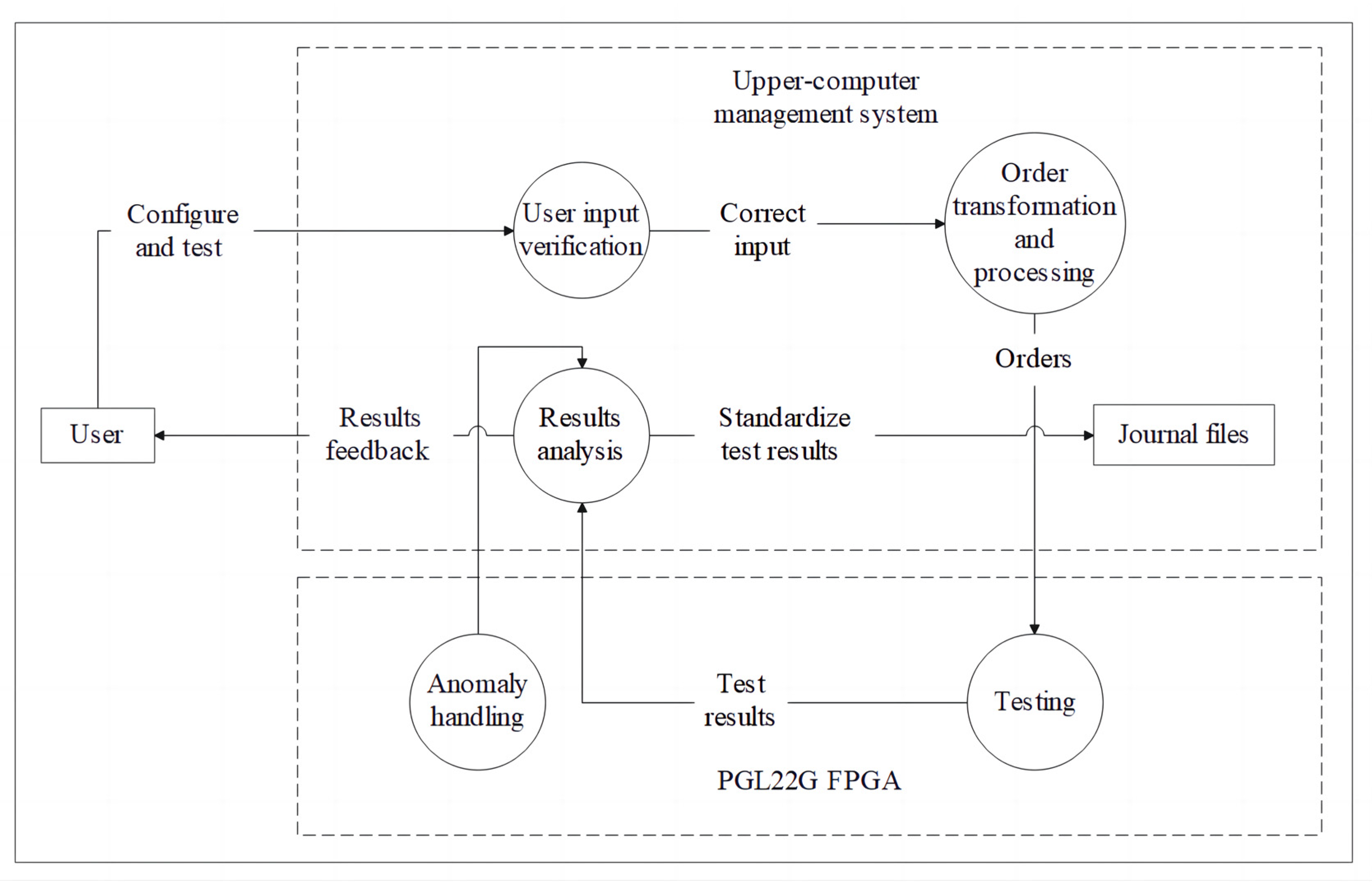
The test system was composed of a host computer, an FPGA test board and USB-UART and JTAG cables. The USB-UART cable was mainly used for data transmission recording by a serial assistant in the host computer, while the JTAG cable was responsible for programming FPGA. The electronic design automation (EDA) software tool, Pango design suite (PDS), was installed on the host computer. The PDS was used to realize the following: the circuit prototype design, synthesis, device map, place and route, bitstream generation and configuration. Moreover, the readback and verify bitstream would be realized with the help of the EDA tool. On the serial port debugging aids of the host computer, the test circuit operational aspect was demonstrated in real time and the movement results of the FPGA were examined. The test results reflect the impact induced by SEEs on an FPGA. The PGL22G FPGA chip mounted on a test board should be unpacked to ensure that the alpha particles can penetrate metal wiring layer to directly access sensitive areas of the semiconductor device before performing the SEE experiment. Based on the system design ideas and design objectives, the design block diagram of the FPGA SEE test system is shown in Figure 5, with the main workflow divided into the following steps:
  • User input and configuration, such as test circuits loading, configuration download, readback and other functions, were accepted by the host computer test management software;
  • The host computer test management software sent test commands, such as bitstream file configuration, to the lower computer FPGA test board;
  • The lower computer FPGA accepted the upper computer command to load the test program and executed the test according to the configuration;
  • The FPGA test board fed back the test results to the upper test management software, which was used to record the test results;
  • For the exceptions that occurred during the execution of the lower FPGA test board, information concerning the exception and its handling were fed back to the test management software of the upper computer.

4.3. Test Procedures

The purpose of conducting the alpha single event effect test is to determine the alpha SEE sensitivity of the main function units and to obtain the alpha particle SEE cross sections. Various test conditions for different modules were illustrated in Table 3. And The test flow, as shown in Figure 6, was as follows:
  • The system was powered up and at the same time the device was configured and the circuit program for the test, which was downloaded to the FPGA test board, was selected;
  • The radiation source was placed horizontally on the surface of the chip under test and the upper computer for the test function was verified;
  • Operation was continuous when the test board operated normally; otherwise, the abnormal data were counted and the FPGA test board was reconfigured;
  • If the number of SEE events exceeded 100 or the alpha fluence exceeded 1 × 10 7 particles · cm 2 , the irradiation test was stopped;
  • The radiation source was removed and the alpha fluence and the number of SEEs were calculated.

5. Experiments Results

The SEE cross sections were calculated according to Equation (1) [24].
σ = N error F ,
where σ is SEE cross section in cm2, N errors is the number of SEE events and F represents the α particle cumulative fluence in particles·cm−2.
The SEU cross section for the memory modules, such as the BRAM and CRAM, can be calculated as follows.
σ seu = # bit _ errors F   ×   Total _ bits   ,
where σ seu is the SEU cross section in cm2/bit, # bit _ errors is the number of bits upset in the BRAM or CRAM, F is the α particle cumulative fluence in particles·cm−2 and Total_bits represent the total measured capacity of the memory module.
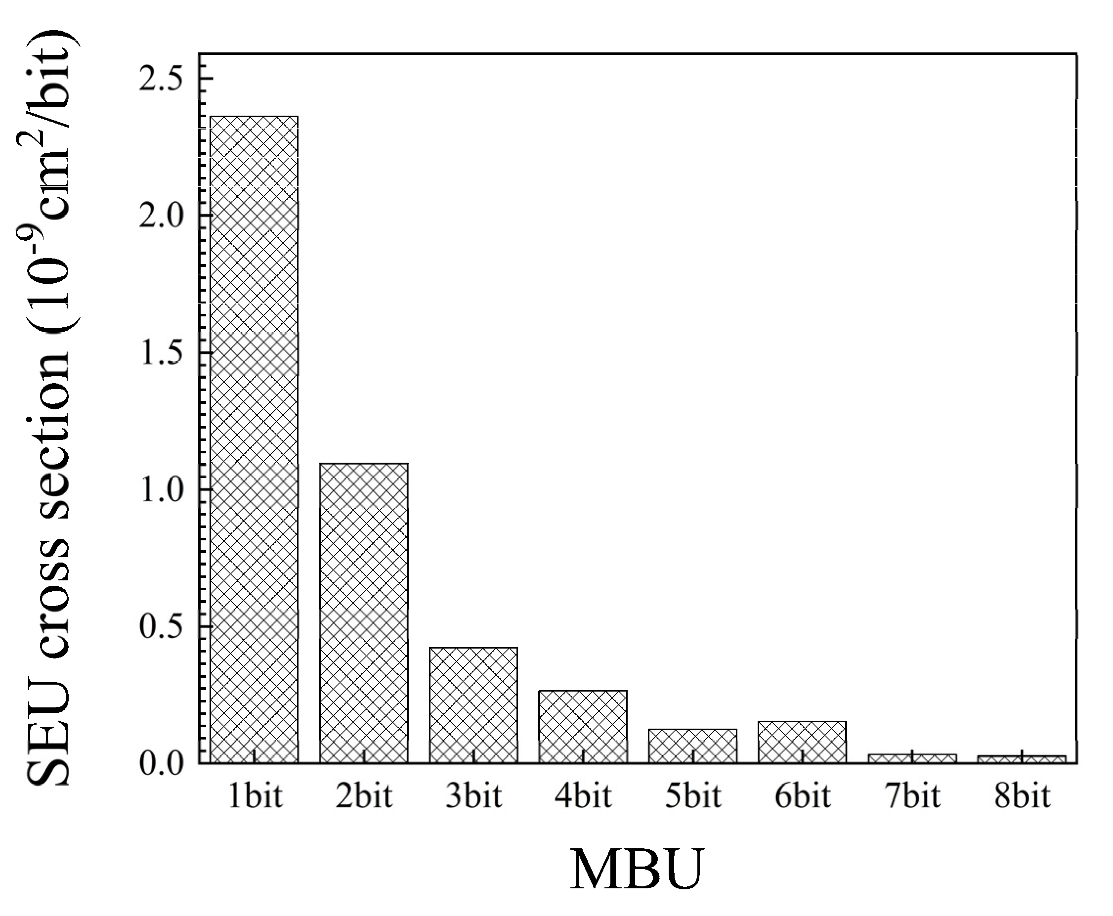
The detailed upset results are shown in Table 4. Both the BRAM and CRAM were based on SRAM cells for data storage. The cross sections of the SEUs for both the CRAM module and the BRAM module were in the order of 10 9 , with the CRAM’s SEU cross section being slightly higher. At the same time, two- to eight-bit upset errors were observed in the CRAM. Of the 762,528 bytes of the configuration memory under test, 357,430 bytes underwent SEU, with a single bit upset (SBU) of 188,513 bytes accounting for 52.7% of the total upsets and multiple bit upset (MBU) of a total of 168,917 bytes accounting for 47.3% of the total upsets. The specific MBU cross section data are shown in Figure 7. Two-bit flips were the most frequent of the MBUs, there being more than forty times as many as there were eight-bit flips. In the process of the experiment, attention was paid to the changes in the signal indicators on the experimental board. It was determined that there was no failure in the readback of the configuration interface during the whole experiment. In other words, there was no SEFI in the CRAM static test. From these experimental data, errors can be categorized into three types:
  • Upset Error: Data errors caused by SBUs and MBUs in the memory module or data register module. The LUT, register cell in the CLM module and the BRAM module were the main areas where SEUs occurred in this experiment.
  • Program Interrupt: The test program was suddenly stopped but could be returned to the normal state through reloading the program in the power state. All program function interrupts in the dynamic test could be recovered by reconfiguration, and no DONE signal dropout was observed. Burst errors induced by the upset of the global registers can be one of the most important reasons for SEFIs in a functional test.
  • Program Corrupt: An unrecognized or unknown output produced by the DUT which can be restored to a normal state by JTAG reconfiguration. Repetitive and unpredictable data upsets were often present in the output of this fault, which was generally considered to be the result of a clock-introduced error. This fault occurred very frequently in the BRAM and CLM testing, and thus should be considered when designing the radiation hardness techniques.

6. Discussion

6.1. Analysis of the Radiation Sensitivity

SEFI is specific to the entire device and typically occurs in the FPGA’s configuration control logic, communication interface control logic, power-on reset circuitry or global logic control circuitry [25]. Once a functional interrupt that is more harmful to the device occurs in this type of functional module, it needs to be recovered by a global reset or re-powering. The usual methods for monitoring SEFIs in the dynamic functional testing of BRAMs and CLMs include DONE signal monitoring and reconfiguration without re-power. While the FPGA was in operation, its DONE signal was high and the JTAG port could read back and configure the FPGA successfully. Conversely, there are three reasons why the program stopped due to alpha particle irradiation. First, the DONE signal changing to low meant that the POR circuit was in SEFI. Second, if reconfiguring the FPGA could not make the FPGA work again with the JTAG port in power, this meant that a SEFI had occurred in the JTAG control signal. However, if the above two circuits were in normal operation, the other control register modules in the design circuit, such as the write signal control register in the FIFO circuit and the shift signal control register in the shift register circuit, were in SEU, causing the program to stop.
Under the radiation of 241Am, faults appeared in the form of SBUs and MBUs in the CRAM module of the DUT. The results show that interconnecting line capital control bits are primarily responsible for configuration memory flips. Isotropic alpha particles deposit energy in one or more sensitive regions of the chip under test while generating a high density of charge–hole pairs, which drift and spread in adjacent sensitive nodes so that a single particle penetrating multiple sensitive regions and severe charge sharing are important causes of MBUs in configuration memory. The bit upset of the configuration memory reached up to eight bits, and the MBU caused by radiation was not negligible. Attention should be paid to this in the hardening design.
For the BRAM module, the data of the block memory were constantly updated so as to reduce the probability of data flipping in the dynamic test. The SEU cross section for the BRAM was smaller than the cross section in the static test. Additionally, a SEFI caused by a global register error has a greater impact on this functional module than a data error caused by an SEU. Errors in the write control registers, communication interface control registers and clock control registers affected by the SEE can lead to direct failure of the BRAM module. In addition, when the program was interrupted during the test and the data output stopped, a read-back verification of the configuration stream showed errors in the underlying configuration memory, suggesting that configuration memory errors caused by single event effects during the test could also lead to program function interruptions in the functional module.
The LUT cells and registers in the CLM are more severely affected by charge sharing, while the influence of bipolar amplification effects also need to be considered [23]. The charge–hole pair generated by the incident particle diffuses and drifts in the presence of an electric field to produce a transient pulse, and the bipolar amplification effect plays an important role in the spreading of the transient pulse width, which increases the chance that the logic flip caused by the propagation of a single event transient current in a logic circuit will be captured by a register. Transient pulses captured by control registers are prone to single event function interruptions, while those captured by one or more data registers are prone to SEUs or MBUs, as shown in Figure 8. Particular attention should be paid to the radiation hardening of the CLM.

6.2. Influences and Strategies

The radiation sensitivity of the PGL22G FPGA is evident based on the results of the alpha experiments. Therefore, some conclusions and recommendations on SEE sensitivity and hardening strategies for the DUT that may be very useful for FPGA users are provided. From the above experimental results and the underlying reasons, it is clear that different methods of radiation reinforcement are required for different modules. For configuration memory modules, the alpha particles mainly cause SEUs on the underlying interconnects, which have a significant impact on the underlying configurable resources and the functionality of the FPGA. The hardening scheme of readback-refresh and reconfiguration can effectively mitigate the impact of the SEE. For BRAM modules, the use of CRC/ECC codes before and after reading/writing data can effectively reduce the upset errors that occur in the BRAM module. In addition, local triple-mode redundancy for some of its internal global control registers can reduce the impact of SEFIs. For CLM modules, which are more affected by single event effects, a triple mode redundancy hardening scheme can be used to cut down the probability of SEUs occurring in this module. Additionally, a timed refresh reconfiguration hardening scheme should also be considered. In terms of the underlying physical structure of the FPGA, dual interlocking memory cells (DICE) are more suitable for replacing standard cells in SEFI sensitive ports [26]. Although fully hardened structures are power-consuming and increases the area of the FPGA, the cross sectional results of SEFIs can be effectively controlled [27]. Moreover, the influence of the MBUs caused by cascade reaction would be another essential issue that needs to be solved before application in a radiation environment.

7. Conclusions

The soft error sensitivity tests for the commercial 40 nm FPGA were performed by alpha particle irradiation using a 241Am source. The results show that the error types induced by the SEEs were upset errors, program interrupts and program corrupts for different functional units. The SEUs and SEFIs were major causes leading to the operational failure of the FPGA. The SEE cross sections of different blocks are presented to guide radiation hardening strategies. It is a great challenge to produce commercial 40 nm devices that work in space radiation environments where protons/heavy ions have larger LETs and higher energy relative to the 241Am source in terms of experiment results. The single event effect research for the FPGA device based on the 40 nm CMOS process was significant.

Author Contributions

Conceptualization, X.D.; methodology, X.D.; software, X.D.; validation, X.D. and X.X.; formal analysis, X.D. and X.X.; investigation, X.D. and X.X.; resources, X.D., B.Z., Z.C., W.J. and S.H.; data curation, X.X. and Y.Z.; writing—original draft preparation, X.X.; writing—review and editing, X.X. and X.D.; visualization, X.X., X.D., B.Z., Z.C. and W.J.; supervision, X.D., B.Z., Z.C. and W.J.; project administration, X.D., Z.C. and W.J.; funding acquisition, X.D., Z.C. and W.J. All authors have read and agreed to the published version of the manuscript.

Funding

This research was supported by the Science and Technology on Reactor System Design Technology Laboratory, grant number HT-KFKT-24-2021004; the Research Foundation of the Education Bureau of Hunan Province, China, grant number 20A430; the Natural Science Foundation of Hunan Province of China, grant number 2021JJ40444 and grant number 2019JJ30019; the science and technology innovation Program of Hunan Province, grant number 2020RC3054; and the Doctoral Research Fund of the University of South China.

Data Availability Statement

Not applicable.

Conflicts of Interest

The authors declare no conflict of interest.

References

  1. Wang, J.J.; Katz, R.B.; Sun, J.S. SRAM based re-programmable FPGA for space applications. IEEE Trans. Nucl. Sci. 1999, 46, 1728–1735. [Google Scholar] [CrossRef] [Green Version]
  2. Montealegre, N.; Merodio, D.; Fernandez, A.; Armbruster, P. In-flight reconfigurable FPGA-based space systems. In Proceedings of the 2015 NASA/ESA Conference on Adaptive Hardware & Systems, Montreal, QC, Canada, 15–18 June 2015; pp. 1–8. [Google Scholar]
  3. Leon, A.F. Field programmable gate arrays in space. IEEE Instrum. Meas. Mag. 2003, 6, 42–48. [Google Scholar] [CrossRef]
  4. Yan, L.; Wang, Q.; Fang, L.; Gu, H.; Li, N. Application of FPGA in space electronics device. J. Space Sci. 2009, 29, 54–58. [Google Scholar]
  5. Normand, E. Single-event effects in avionics. IEEE Trans. Nucl. Sci. 1996, 43, 461–474. [Google Scholar] [CrossRef]
  6. Normand, E.; Oberg, D.L.; Wert, J.L.; Ness, J.D.; Majewski, P.P.; Wender, S.; Gavron, A. Single event upset and charge collection measurements using high energy protons and neutrons. IEEE Trans. Nucl. Sci. 1994, 41, 2203–2209. [Google Scholar] [CrossRef]
  7. Koga, R. Single-event effect ground test issues. IEEE Trans. Nucl. Sci. 1996, 43, 661–670. [Google Scholar] [CrossRef]
  8. White, D. Considerations surrounding single event effects in FPGAs, ASICs, and processors. Xilinx White Pap, WP402 (v1.0.1) March 7. 2012. Available online: https://www.xilinx.com/content/dam/xilinx/support/documents/white_papers/wp402_SEE_Considerations.pdf. (accessed on 28 October 2022).
  9. Cabanas-Holmen, M.; Cannon, E.H.; Amort, T.; Ballast, J.; Brees, R.; Fischer, S.; Kleinosowski, A.J.; Meaker, B.; Swann, T.; Wert, J. Predicting the Single-event Error Rate of a Radiation Hardened by Design Microprocessor. IEEE Trans. Nucl. Sci. 2011, 58, 2726–2733. [Google Scholar] [CrossRef]
  10. Rezgui, S.; Louris, P.; Sharmin, R. SEE Characterization of the New RTAX-DSP (RTAX-D) Antifuse-based FPGA. IEEE Trans. Nucl. Sci. 2010, 57, 3537–3546. [Google Scholar] [CrossRef]
  11. George, J.; Koga, R.; Swift, G.; Allen, G.; Carmichael, C.; Tseng, C.W. Single Event Upsets in Xilinx Virtex-4 FPGA Devices. In Proceedings of the 2006 IEEE Radiation Effects Data Workshop, Ponte Vedra Beach, FL, USA, 17–21 July 2006; pp. 109–114. [Google Scholar]
  12. Quinn, H.; Morgan, K.; Graham, P.; Krone, J.; Caffrey, M. Static Proton and Heavy Ion Testing of the Xilinx Virtex-5 Device. In Proceedings of the 2007 IEEE Radiation Effects Data Workshop, Honolulu, HI, USA, 23–27 July 2007; pp. 177–184. [Google Scholar]
  13. Hiemstra, D.M.; Kirischian, V. Single Event Upset Characterization of the Virtex-6 Field Programmable Gate Array Using Proton Irradiation. In Proceedings of the 2012 IEEE Radiation Effects Data Workshop, Miami, FL, USA, 16–20 July 2012; pp. 1–4. [Google Scholar]
  14. Du, B.; Sterpone, L.; Azimi, S.; Codinachs, D.M.; Ferlet-Cavrois, V.; Polo, C.B.; Alía, R.G.; Kastriotou, M.; Fernandez-Martínez, P. Ultrahigh Energy Heavy Ion Test Beam on Xilinx Kintex-7 SRAM-Based FPGA. IEEE Trans. Nucl. Sci. 2019, 66, 1813–1819. [Google Scholar] [CrossRef]
  15. Lee, D.S.; Allen, G.R.; Swift, G.; Cannon, M.; Wirthlin, M.; George, J.S.; Koga, R.; Huey, K. Single-Event Characterization of the 20 nm Xilinx Kintex UltraScale Field-Programmable Gate Array under Heavy Ion Irradiation. In Proceedings of the 2015 IEEE Radiation Effects Data Workshop (REDW), Boston, MA, USA, 13–17 July 2015; pp. 1–6. [Google Scholar]
  16. Koga, R.; Davis, S.; George, J.; Zakrzewski, M.; Mabry, D. Heavy Ion and Proton Induced Single Event Effects on Xilinx Zynq UltraScale+ Field Programmable Gate Array (FPGA). In Proceedings of the 2018 IEEE Radiation Effects Data Workshop (REDW), Waikoloa, HI, USA, 16–20 July 2018; pp. 1–5. [Google Scholar]
  17. Autran, J.L.; Munteanu, D.; Roche, P.; Gasiot, G.; Martinie, S.; Uznanski, S.; Sauze, S.; Semikh, S.; Yakushev, E.; Rozov, S.; et al. Soft-errors induced by terrestrial neutrons and natural alpha-particle emitters in advanced memory circuits at ground level. Microelectron. Reliab. 2010, 50, 1822–1831. [Google Scholar] [CrossRef]
  18. Baumann, R.C. Radiation-induced soft errors in advanced semiconductor technologies. IEEE Trans. Device Mater. Reliab. 2005, 5, 305–316. [Google Scholar] [CrossRef]
  19. Logos Family FPGA Device Data Guide Sheet. Pangomicro: Shenzhen, China. (DS02001, Version2.2), 2020. Available online: https://www.pangomicro.com/upload/support/file. (accessed on 28 October 2022).
  20. Keller, A.M.; Whiting, T.A.; Sawyer, K.B.; Wirthlin, M.J. Dynamic SEU sensitivity of designs on two 28-nm SRAM-based FPGA architectures. IEEE Trans. Nucl. Sci. 2017, 65, 280–287. [Google Scholar] [CrossRef]
  21. Logos Series FPGA Dedicated RAM Modules (DRM) User Guides. Pangomicro: Shenzhen, China. (UG020002, Version1.1), 2018. Available online: https://www.pangomicro.com/upload/support/file (accessed on 28 October 2022).
  22. Zhang, Z.G.; Ye, B.; Ji, Q.G.; Guo, J.L.; Xi, K.; Lei, Z.F.; Huang, Y.; Peng, C.; He, Y.J.; Liu, J.; et al. Mechanisms of alpha particle induced soft errors in nanoscale static random access memories. Acta Phys. Sin. 2020, 69, 136103. [Google Scholar] [CrossRef]
  23. JESD89A Measurement and Reporting of Alpha Particle and Terrestrial Cosmic Ray-Induced Soft Errors in Semiconductor Devices JEDEC standard, JEDEC Solid State Technology Association: South Arlington, VA USA, 2006. Available online: https://www.jedec.org/ (accessed on 28 October 2022).
  24. Berg, M.; Kim, H.; Phan, A.; Seidleck, C.; Label, K.; Campola, M. Xilinx Kintex-UltraScale Field Programmable Gate Array Single Event Effects (SEE) Heavy-ion Test Report. NASA Electronic Parts and Packaging (NEPP): Washington, USA. 2018. Available online: https://nepp.nasa.gov/pages/pubs.cfm. (accessed on 28 October 2022).
  25. Cai, C.; Gao, S.; Zhao, P.; Yu, J.; Zhao, K.; Xu, L.; Li, D.; He, Z.; Yang, G.; Liu, T.; et al. SEE Sensitivity Evaluation for Commercial 16 nm SRAM-FPGA. Electronics 2019, 8, 1531. [Google Scholar] [CrossRef] [Green Version]
  26. Li, T.; Yang, H.; Cai, G.; Zhi, T.; Li, Y. A CMOS triple inter-locked latch for SEU insensitivity desige. IEEE Trans. Nucl. Sci. 2014, 61, 3265–3273. [Google Scholar] [CrossRef]
  27. Cai, C.; Fan, X.; Liu, J.; Li, D.; Liu, T.; Ke, L.; Zhao, P.; He, Z. Heavy-ion induced single event upsets in advanced 65 nm radiation hardened FPGAs. Electronics 2019, 8, 323. [Google Scholar] [CrossRef]
Figure 1. A picture of the PGL22G FPGA development board (unpacked chip).
Electronics 11 03844 g001
Figure 2. SEE detection process for configuration RAM.
Electronics 11 03844 g002
Figure 3. SEE test circuit design for block RAM.
Electronics 11 03844 g003
Figure 4. The LET and range of α particles in silicon varies with energy.
Electronics 11 03844 g004
Figure 5. The structure chart of the testing system.
Electronics 11 03844 g005
Figure 6. Single event effect dynamic test flow.
Electronics 11 03844 g006
Figure 7. The cross section of the MBU for the CRAM in the static test.
Electronics 11 03844 g007
Figure 8. The cross section of the MBU for the CLM in the dynamic test.
Electronics 11 03844 g008
Table 1. List of resources for the PGL22G FPGA.
DeviceCLM18 Kb BRAMAPMPLLADCHMEMCIO
LUT5FFDistributed RAM
PGL22G17,53626,30471,0404830612240
Table 2. Radiation source parameters used in the experiment.
ParameterValue
Radiation source241Am
Source number14AM4R2031
Emissivity ( particles / 2 π · minute ) 1.21 10 6
Diameter (mm)35
Thickness (mm)1.0
ShapeCylinder
Table 3. Various test conditions for different modules of the device under test.
DUTTest ModuleTest CapacityTest MethodTest Duration
PGL22GCRAM610,024 bitStatic test11 h 46 min
BRAM811,008 bitDynamic test10 h 6 min 19 s
CLB5120 bitDynamic test10 h 10 min 7 s
Table 4. The experiment results for the PGL22G FPGA.
Test ModuleEvent TypeTotal Number of EventsFluence
( p a r t i c l e s / c m 2 )
Cross Section
CRAMUpset Error706,164 1.413 × 10 7 8.193 × 10 9   cm 2 / bit
BRAMProgram Interrupt95 1.214 × 10 7 7.825 × 10 6   cm 2 / device
Program Corrupt89 7.331 × 10 6   cm 2 / device
Upset Error20,668 2.099 × 10 9   cm 2 / bit
CLMProgram Interrupt144 1.221 × 10 7 1.189 × 10 5   cm 2 / device
Program Corrupt25 2.064 × 10 6   cm 2 / device
Upset Error1011 1.617 × 10 8   cm 2 / bit
Publisher’s Note: MDPI stays neutral with regard to jurisdictional claims in published maps and institutional affiliations.