Abstract
Skin and cancer cell treatments using high-intensity focused ultrasound (HIFU) have garnered considerable attention as a technology with fewer side effects. Hence, various schemes have been developed to operate ultrasound transducers with high efficiencies. Class DE power amplifiers operate in zero-voltage switching (ZVS) and zero-derivative switching (ZDS); therefore, high-efficiency operation is possible. However, during the CMOS process, a difference in efficiency arises depending on the gate oxide process, which has not yet been analyzed. In high-power devices, a thick oxide layer is primarily used to prevent breakdown. However, this can lead to a decrease in power efficiency. This study analyzes the overall power consumption for each oxide layer thickness during the AMS H35 CMOS process and compares its efficiency. The results confirm that an output power of approximately 1.8 W and a power efficiency of 94% can be obtained with just a relatively thin gate oxide thickness of approximately 10 nm. Furthermore, an additional power efficiency of approximately 3% can be obtained by reducing only the gate oxide thickness.
1. Introduction
High-intensity focused ultrasound (HIFU) technology is a non-invasive surgical technique that uses ultrasound to treat skin and cancers [1]. For HIFU applications, the driver is preferred to be located near the transducer. The HIFU driver is a self-contained power supply which regulates the power required for the transducer or array of transducers. Moreover, a structure without an inductor in the driver is helpful when using magnetic resonance imaging (MRI) [2,3]. MRI-guided focused ultrasound (MRI-HIFU) was studied for bone metastases pain treatments [4]. To this end, CMOS integration technology has been used to drive multiple transducers [5,6]. This could be of great help in creating catheter ablation systems in the future [7,8]. Also, most of the commercial ultrasonic transducers today are based on piezoelectricity. However, compared to piezoelectricity, the capacitive micromachined ultrasonic transducer (CMUT) process is easy to integrate with other CMOS circuits, including drivers, and has been studied a lot recently [5]. A representative treatment using HIFU is prostate cancer treatment because heat is applied only to the desired area [9,10]. HIFU treatment destroys cancerous tissue by inserting an HIFU device into the body through the anus and generating heat above 80 °C [9]. Although surgery is the basic treatment for prostate cancer, HIFU treatment can be an effective alternative for patients who have difficulty with surgery due to regional prostate cancer, age, or comorbidities [10,11]. HIFU treatment is virtually painless and can be performed only once [11]. Above all, using HIFU treatment, the urination and sexual functions can be effectively preserved [12,13]. In addition, there are no restrictions on retreatment; therefore, it is highly preferred method for patients with early cancer. Based on the fusion image overlaid with MRI, the image can be checked in real-time during treatment, and the rectal wall can be automatically recognized using ultrasound to locate the treatment area accurately [11]. Therefore, it has few side effects and enables a quick return to daily life after treatment. In practical applications, HIFU has a good prognosis for treating prostate cancer and has shown great success [14]. However, for HIFU treatment, heat must be applied to the correct area, and the effect must be small in other areas; therefore, the array form is preferred. A phased array is used to not only steer the beam but to avoid heating sensitive structures. To achieve constant efficiency in these multi-array cells, several control algorithms have been developed [15].
Recently, class DE amplifiers rather than linear amplifiers have been proposed for driving circuits to reduce the internal temperature and increase efficiency. A power amplifier is a key component that determines the performance of a transducer driver [16,17]. In order to have high-power driving and high-power efficiency, research is being conducted on GaN devices in addition to CMOS devices [18]. In the driving topology, there were efforts to lower the high DC voltage bias [19,20] and to simultaneously control a large array [21,22]. There were also attempts to increase the range of operating frequencies [23] and to try to implement them digitally [24,25]. Research analyzing the problems in practical application [26] are also being made. However, for catheter ablation systems, research to minimize the generation of additional heat by achieving high power efficiencies is essential. A recent study used a class AB topology to design a high-bandwidth linear amplifier with approximately 50% power efficiency for medical ultrasonic transmitter applications [27]. The class AB topology has the advantage of obtaining a linear signal. However, it operates in a push-pull type manner, and its power efficiency is lower than that of the class B topology. However, in the case of a single element, a class DE power amplifier can achieve a power efficiency of approximately 90% [28,29,30]. This is possible because in the case of switched amplifiers, the power loss can be reduced through zero-voltage switching (ZVS) with the assistance of zero-derivative switching (ZDS) operation. The total transmitted power may have a disadvantage in that it has a low value in terms of the duty ratio, but the power efficiency is very high, so it is suitable for the catheter ablation-type application.
It is noted that the previously proposed class DE structure has the advantage of enabling a gate swing of 20 V, using a thick oxide for the driver circuit. However, this increases the gate loss (PG) owing to the large gate voltage swing [31]. In the case of a class DE amplifier, the gate voltage swing is not limited to VDD [32]. Essentially, the gate oxide thickness affects the gate voltage swing and the overall efficiency of the power amplifier. To analyze this effect, the overall power loss according to the gate oxide thickness of the driver circuit was compared in this study. Although a multi-element comparison is possible, a case wherein one element operates as an ideal class DE amplifier was considered. All the verification processes were performed based on the physical and electrical parameters of the AMS H35 CMOS process. Through this study, the optimal structure of the gate driver circuit according to the thickness of the gate oxide was confirmed, and the effect on the power efficiency was analyzed.
2. Experiments and Results
Fundamentally, the total power loss in a power amplifier is defined as follows.
where Ploss is the total power loss; Pconduction is the conduction power loss; PS is the switching power loss; and PG is the gate loss, which includes the gate driver power loss. As the switching speed increases, PS and PG increase significantly. In class DE amplifiers, PS can be significantly reduced through ZVS and ZDS operations. To reduce Pconduction, new materials, such as GaN, can be used as a low-drain source of resistance (Rds,on). However, GaN devices are difficult to integrate into gate driver circuits; nonetheless, they can be used to drive high-power transducers. Therefore, for the case of a CMOS process and class DE amplifier, Pconduction occupies the largest portion. Moreover, Pconduction is simply the product of the current flowing through a switch when it is forward-biased, and the voltage drops across it. To reduce this Pconduction, various processes, such as CoolMOS from Infineon, are being developed in the CMOS process [33].
Ploss = Pconduction + PS + PG,
In this study, the simulation was performed using the AMS 0.35 μm 50 V process. The gate oxides capable of 50 V VDS provided by the AMS H35 process were thick, mid, and thin oxides. The thickness of the thick oxide was approximately 50 nm, and that of the thin oxide was approximately 10 nm. The gate voltage swings of the thick gate, mid gate, and thin gate oxides could be realized up to 20, 5, and 3.3 V, respectively. Figure 1 shows the basic structure of the class DE power amplifier. An equivalent model of the piezoelectric transducer was placed under the load. The structure was in the form of a full bridge to increase output power. The power transistors used for the nMOS and pMOS were sized to have similar switching speeds. The gate voltage swing of the driver varied according to the gate-oxide thickness. In the case of the class DE amplifier, switching of the amplifier was performed according to the transducer’s resonance frequency. The series inductance (Ls), series capacitance (Cs), series resistance (Rs), and parallel capacitance (Cp) of the piezoelectric transducer-equivalent model of a single-element structure for the simulation were 315 µH, 90 pF, 55 ohm, and 950 pF, respectively [30]. Using a class DE amplifier is a method that actively utilizes the resonance frequency of the load. In this case, the duty ratio (D) and conduction angle (φ) for the ZVS or ZDS operation can be determined using the following equation [29]:
where δ is ΔV/V, which represents the voltage overshoot during the switching sequence. For ZVS operation, ΔV must be equal to zero. In an ideal case, ZVS, ZDS, and high efficiencies are achieved. However, only some transducer elements can operate as ideal class DE amplifiers when driving multiple transducer elements. D was used primarily at approximately 25%. The calculated D, φ, and f values were 0.26, 1.5, and 966 kHz, respectively. Furthermore, ZVS and ZDS operations could be realized through these operations, and the PS could be lowered. Digital logic was used to generate the output of the pulse generator, the D and f values were adjusted, and the output voltage was fixed at 3.3 V for comparison. The voltage, VDD, was fixed at 22 V for high-power delivery.

Figure 1.
Schematic of full bridge class DE power amplifiers.
When a thick gate oxide is used in the power amplifier, a gate swing of 20 V is required for the low-side gate driver. Similarly, mid and thin gate oxides require gate voltage swings of 5 V and 3.3 V, respectively. Therefore, in this study, the structure of the low-side gate driver was configured differently to minimize power consumption according to the gate oxide thickness. A thin gate oxide can be configured only in the form of two inverters. This structure was configured by optimizing the size of the device to drive a large capacitance; additionally, it had the lowest static power loss. In the case of the mid-thickness gate oxide, the input of the pulse generator was converted from 3.3 V to 5 V using a simple level shifter. In this case, a cross-coupled structure was used, with the disadvantage that static loss continues to occur. Similar to this structure, in the case of a thick gate oxide, a cross-coupled level shifter was used, which generated a gate voltage swing of 20 V. Figure 2 depicts the proposed structure of the low-side gate driver depending on the gate oxide thickness. Figure 2a,b show a low-side gate driver with a thick and mid-thickness gate oxide, respectively, and have a cross-coupled structure. Figure 2c shows a low-side gate driver in thin gate oxide and has an inverter structure. Although the level shifter structure has the advantage of being able to generate a high voltage easily, it has the disadvantage of exhibiting static power loss. An optimal structure based on the operating voltage is proposed in Figure 2. “In” signal indicates the input voltage from the pulse generator. In the case of the low-side gate driver, the voltage swing has a large difference; therefore, it significantly affects PG.
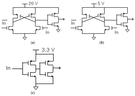
Figure 2.
Schematic of low-side gate driver: (a) thick gate oxide, (b) mid-thickness gate oxide, (c) thin gate oxide.
The power consumption with load for low-side gate drivers using thick, mid, and thin gate oxides was 7.89 mW, 1.17 mW, and 0.69 mW, respectively. In the case of low-side gate drivers, a low gate voltage swing has a significant advantage in terms of power consumption. Because two drivers are used for the low side-gate driver, they consume twice the power mentioned above.
The configuration becomes more complicated in the case of a high-side gate driver. To drive the power transistors of the PMOS, a gate swing from 22 V to 2 V, from 22 V to 17 V, and from 22 V to 18.7 V should be made for thick-gate oxide, mid-gate oxide, and thin-gate oxide devices, respectively. In the case of the thick gate oxide, a structure similar to the previous one was used for comparison [31]. When designing a high-side gate driver, a cross-coupled structure similar to that of a level shifter was used. “In” signal indicates the input voltage from the pulse generator. In this case, a cross-coupled structure was used and static loss occurred. The inverter structure at the backstage was used to drive a high capacitance and generate the desired voltage for a high-side gate driver. The average power consumption of this gate driver was 13.87 mW (Figure 3a). However, note that when the same structure is used for mid or thin gate oxides, the power transistor pMOS in the full-bridge structure does not turn on. This is because the gate voltage swing difference for the turn-on and turn-off of the pMOS power transistor is too small in mid and thin gate oxides. To prevent this in the case of mid and thin gate oxides, the high-side gate driver was configured in the form of a voltage divider using resistors (R1 and R2). In this case, similar to the cross-coupled structure, static loss occurs; however, this loss can be minimized by increasing the resistance (Figure 3b,c). High resistance can increase the turn-on delay; therefore, an optimization process is required. Thus, the total gate loss became approximately 12.61 mW for the mid gate oxide and 9.44 mW for the thin gate oxide. In the case of a high-side gate driver, the reduction in the gate voltage swing does not have a significant effect on power reduction. The voltage divider structure enables a simple configuration and fast switching speed; therefore, it can have a switching delay within 2 ns. Essentially, the switching voltage range is very important for the structure of a high-side gate driver. When the switching voltage range is large, the cross-coupled structure is advantageous in speed and power consumption. When the switching voltage range is small, the voltage divider structure is advantageous in speed and power consumption.
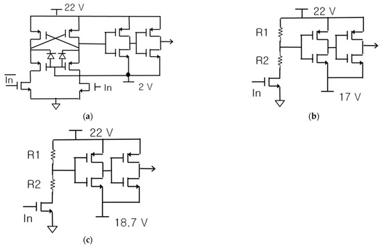
Figure 3.
Schematic of high-side gate driver: (a) thick gate oxide, (b) mid gate oxide, (c) thin gate oxide.
Finally, Pconduction and PS were verified. Pconduction can be determined using the following equation:
where IDS is the drain current between the source and drain during the on state, which is not constant. For an accurate comparison, the total area of the power amplifier was fixed at the same value because Rds,on can be reduced in proportion to the total area. In the case of thick-gate oxide devices, the approximate values of Rds,on, Pconduction, and PS were 4.5 ohm, 32.8 mW, and 0.64 mW, respectively, for one transistor. Each PS for various gate oxide thicknesses can be calculated by integrating the currents during switching times. Figure 4 shows the waveforms of the drain currents for the high-voltage pMOS. The load currents are also shown for better understanding. Evidently, the peak load currents were slightly higher for the thin-gate oxide devices. In the case of mid-gate oxide and thin-gate oxide devices, the approximate values of Rds,on, Pconduction, and PS were 3.5 ohm, 23.92 mW, and 0.32 mW; and 3.5 ohm, 24.1 mW, and 0.36 mW for one transistor, respectively. These values were similar for high-power nMOS and pMOS. Under a similar VDS, as depicted in Figure 4, the main factor for reduced Pconduction in mid- and thin-gate oxide devices is the reduced Rds,on.
Pconduction = Rds,on × IDS2,
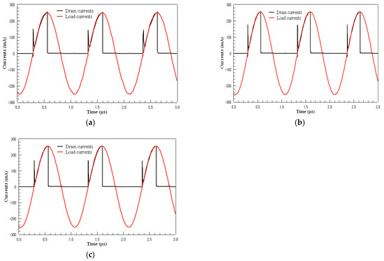
Figure 4.
Waveforms of the PMOS drain currents and the load currents for Pconduction and PS calculations: (a) thick gate oxide, (b) mid gate oxide, (c) thin gate oxide.
Rds,on, which is proportional to 1/IDS in the linear region, tends to decrease significantly because the gate oxide capacitance per unit area (Cox’) and effective mobility (µeff) increase as the gate oxide thickness decreases in a high-voltage CMOS. However, Rds,on tends to increase slightly because the gate overdrive voltage (VGS-Vth) decreases as the gate oxide thickness decreases in a high-voltage CMOS. IDS of the MOSFET in the linear region is modeled as follows:
where L and W are the channel length and width, respectively. However, because several model parameters affect IDS and Rds,on, the trends of IDS and Rds,on, according to the gate oxide thickness, may vary depending on the fabrication process. In the case of the AMS H35 process, a low Rds,on can be obtained through optimization without affecting the operation by reducing the gate oxide thickness, even when the total area is the same. This is because the increases in Cox’ and µeff are greater than the decrease in the gate overdrive voltage when the gate oxide thickness decreases. Therefore, Rds,on can be reduced in mid- and thin-gate oxide devices.
In the class DE power amplifiers, PS is significantly smaller than Pconduction. This is because the class DE power amplifier operates in ZVS and ZDS. A very small PS was observed for devices with all gate oxide thicknesses. CMOS drain currents drive only approximately 26% of the entire waveform, and the voltage is slowly decreased by Cp of the load stage, thereby creating a total sine wave. In this process, noise components, such as harmonic components, have very small values. In this case, the drain current of the CMOS exhibited power loss during switching. However, this value was not observed in the load currents owing to the tuning effect of the load. Table 1 lists the total loss and power efficiency for gate oxide thickness. The power consumption of the pulse generator module was assumed to be 3 mW, which was added to the PG.

Table 1.
Summary of overall power loss and power efficiency with different gate oxide technologies.
Although there was a slight difference in the power consumption depending on the piezoelectric transducer, we obtained similar results. Among Ploss, PS is very small because it operates as ZVS and ZDS in a class DE amplifier. The power efficiency can be further increased using a gate oxide with a low gate thickness and lowering the gate voltage swing. The PG can be lowered to approximately 23 mW when a thin gate oxide is used. In addition, the Pconduction can be lowered with mid- and thin-gate oxide devices. The efficiency of the class DE amplifier was improved by reducing the gate voltage swing and the gate oxide thickness.
The achievable power efficiency of thin-gate oxide devices was approximately 93.7%, which reduced the effect of reducing heat generation of the entire chip. In the case of the class DE amplifier, PG power loss reduction was achieved without affecting the operation of the power amplifier using a thin gate oxide process. The overall power loss is plotted against different oxide thicknesses for each component (Figure 5).
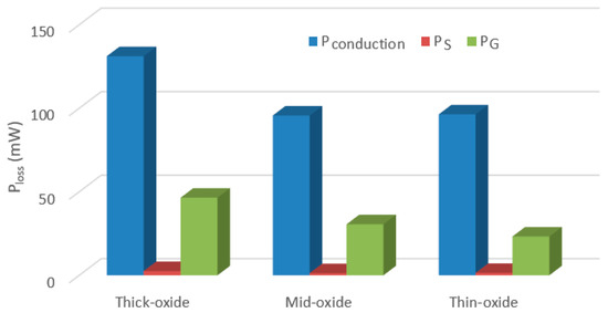
Figure 5.
Ploss diagram against different oxide thicknesses.
These results confirm that the ratio of Pconduction to Ploss was high in the case of the class DE amplifier. Evidently, process development of the power devices is required to reduce this. In addition, Pconduction decreased in the AMS H35 CMOS process by reducing the gate oxide thickness. In terms of circuit design, the PG can be reduced, and static loss must be reduced. This approach can be achieved by reducing the gate voltage swing using a thin oxide layer, which can contribute to reducing the overall loss. Moreover, various circuit approaches are possible. In particular, by suggesting structures suitable for gate voltage in this study, it will help realize low-power circuits for HIFU applications in future studies.
3. Conclusions
CMOS processes can achieve high efficiency because they can be easily integrated into a single chip to operate in HIFU applications. In particular, a high-efficiency class DE CMOS power amplifier was proposed. This study analyzed the power efficiency based on the gate oxide thickness in a class DE power amplifier. In this case, using the thin gate oxide process for a low gate swing, PG and Pconduction could be reduced to 23 mW and 96 mW, respectively. An overall power efficiency was achieved at approximately 93.7%. Thus, a transducer driver that generates less heat can be manufactured using thin-gate oxide device. In addition, an optimal structure in terms of the power loss according to each gate oxide thickness was proposed for further studies. This structure will be suitable for catheter ablation-type applications, and it is planned to perform power-efficiency increase analysis in array types in the future.
Author Contributions
Conceptualization, H.-S.C. and T.N.; Methodology, H.-S.C. and Y.Z.; Validation, H.-S.C., T.N. and Y.Z.; formal analysis, Y.Z.; investigation, H.-S.C.; resources, Y.Z.; data curation, H.-S.C.; writing—original draft preparation, H.-S.C.; writing—review and editing, Y.Z.; visualization, H.-S.C.; supervision, Y.Z.; project administration, Y.Z.; funding acquisition, H.-S.C. All the authors have read and agreed to the published version of the manuscript. All authors have read and agreed to the published version of the manuscript.
Funding
This study was supported by a research fund from the Chosun University (2020).
Institutional Review Board Statement
Not applicable.
Informed Consent Statement
Not applicable.
Data Availability Statement
Not applicable.
Acknowledgments
This study was supported by a research fund from the Chosun University (2020).
Conflicts of Interest
The authors declare no conflict of interest.
References
- Sanchez, M.; Barrere, V.; Treilleux, I.; Chopin, N.; Melodelima, D. Development of a noninvasive HIFU treatment for breast adenocarcinomas using a toroidal transducer based on preliminary attenuation measurements. Ultrasonics 2021, 115, 106459. [Google Scholar] [CrossRef] [PubMed]
- Yee, C.H.; Chiu, P.K.F.; Teoh, J.Y.C.; Ng, C.F.; Chan, C.K.; Hou, S.M. High-intensity focused ultrasound (HIFU) focal therapy for localized prostate cancer with MRI-US fusion platform. Adv. Urol. 2021, 2021, 7157973. [Google Scholar] [CrossRef] [PubMed]
- Yu, L.; Zhu, S.; Zhang, H.; Wang, A.; Sun, G.; Liang, J.; Wang, X. The efficacy and safety of MR-HIFU and US-HIFU in treating uterine fibroids with the volume <300 cm3: A meta-analysis. Int. J. Hyperth. 2021, 38, 1126–1132. [Google Scholar] [CrossRef] [PubMed]
- Bongiovanni, A.; Foca, F.; Oboldi, D.; Diano, D.; Bazzocchi, A.; Fabbri, L.; Mercatali, L.; Vanni, S.; Maltoni, M.; Bianchini, D.; et al. 3-T magnetic resonance-guided high-intensity focused ultrasound (3 T-MR-HIFU) for the treatment of pain from bone metastases of solid tumors. Support. Care Cancer 2022, 30, 5737–5745. [Google Scholar] [CrossRef] [PubMed]
- Joseph, J.; Ma, B.; Khuri-Yakub, B.T. Applications of capacitive micromachined ultrasonic transducers: A comprehensive review. IEEE Trans. Ultrason. Ferroelectr. Freq. Control 2022, 69, 456–457. [Google Scholar] [CrossRef] [PubMed]
- Brenner, K.; Ergun, A.S.; Firouzi, K.; Rasmussen, M.F.; Stedman, Q.; Khuri-Yakub, B. Advances in capacitive micromachined ultrasonic transducers. Micromachines 2019, 10, 152. [Google Scholar] [CrossRef]
- Bozkurt, A.; Farhanieh, O.; Roy, R.B.; Ergun, A.S. Design of a driver IC for an ultrasound catheter ablation system. In Proceedings of the 2014 IEEE International Ultrasonics Symposium, Chicago, IL, USA, 3–6 September 2014; pp. 1536–1539. [Google Scholar]
- Bui, N.T.; Nguyen, T.M.T.; Ataklti, G.Y.; Bui, Q.C.; Dinh, T.T.N.; Phan, D.T.; Park, S.; Choi, J.; Vu, T.T.H.; Oh, J. Design of a High-Power Multilevel Sinusoidal Signal and High-Frequency Excitation Module Based on FPGA for HIFU Systems. Electronics 2021, 10, 1299. [Google Scholar] [CrossRef]
- Aus, G. Current status of HIFU and cryotherapy in prostate cancer—A review. Eur. Urol. 2006, 50, 927–934. [Google Scholar] [CrossRef]
- Cordeiro, E.R.; Cathelineau, X.; Thueroff, S.; Marberger, M.; Crouzet, S.; de la Rosette, J.J. High-intensity focused ultrasound (HIFU) for definitive treatment of prostate cancer. BJU Int. 2012, 110, 1228–1242. [Google Scholar] [CrossRef]
- Panzone, J.; Byler, T.; Bratslavsky, G.; Goldberg, H. Transrectal Ultrasound in Prostate Cancer: Current Utilization, Integration with mpMRI, HIFU and Other Emerging Applications. Cancer Manag. Res. 2022, 14, 1209. [Google Scholar] [CrossRef]
- Bakavicius, A.; Marra, G.; Macek, P.; Robertson, C.; Abreu, A.L.; George, A.K.; Malavaud, B.; Coloby, P.; Rischmann, P.; Moschini, M.; et al. Available evidence on HIFU for focal treatment of prostate cancer: A systematic review. BJU Int. 2022, 48, 263–274. [Google Scholar] [CrossRef] [PubMed]
- Maestroni, U.; Tafuri, A.; Dinale, F.; Campobasso, D.; Antonelli, A.; Ziglioli, F. Oncologic outcome of salvage high-intensity focused ultrasound (HIFU) in radiorecurrent prostate cancer. A systematic review. Acta Bio Med. Atenei Parm. 2021, 92, 2021191. [Google Scholar]
- Dellabella, M.; Branchi, A.; Di Rosa, M.; Pucci, M.; Gasparri, L.; Claudini, R.; Carnevali, F.; Cecchini, S.; Castellani, D. Oncological and functional outcome after partial prostate HIFU ablation with focal-one®: A prospective single-center study. Prostate Cancer Prostatic Dis. 2021, 24, 1189–1197. [Google Scholar] [CrossRef] [PubMed]
- Zubair, M.; Dickinson, R. Calculation the effect of ribs on the focus quality of a therapeutic spherical random phased array. Sensors 2021, 21, 1211. [Google Scholar] [CrossRef]
- Jang, J.H.; Rasmussen, M.F.; Bhuyan, A.; Yoon, H.S.; Moini, A.; Chang, C.; Watkins, R.D.; Choe, J.W.; Nikoozadeh, A.; Stephens, D.; et al. Dual-mode integrated circuit for imaging and HIFU with 2-D CMUT arrays. In Proceedings of the 2015 IEEE International Ultrasonics Symposium (IUS), Taipei, Taiwan, 21–24 October 2015. [Google Scholar]
- El-Desouki, M.M.; Hynynen, K. Driving Circuitry for Focused Ultrasound Noninvasive Surgery and Drug Delivery Applications. Sensors 2011, 11, 539–556. [Google Scholar] [CrossRef] [PubMed]
- Carpenter, T.M.; Cowell, D.M.J.; Clegg, H.R.; McLaughlan, J.R.; Freear, S. High-Power Gallium Nitride HIFU Transmitter with Integrated Real-Time Current and Voltage Measurement. IEEE Trans. Biomed. Circuits Syst. 2021, 15, 270–280. [Google Scholar] [CrossRef]
- Takagi, R.; Yoshinaka, K.; Washio, T.; Koseki, Y. A visualization method for a wide range of rising temperature induced by high-intensity focused ultrasound using a tissue-mimicking phantom. Int. J. Hyperth. 2022, 39, 22–33. [Google Scholar] [CrossRef]
- Merbeler, F.; Wismath, S.; Haubold, M.; Bretthauer, C.; Kupnik, M. Ultra-Low-Voltage Capacitive Micromachined Ultrasonic Transducers with Increased Output Pressure Due to Piston-Structured Plates. Micromachines 2022, 13, 676. [Google Scholar] [CrossRef]
- Poongodan, P.K.; Sakolski, O.; Vanselow, F.; Maurer, L. An 8 Channel Transceiver ASIC to Interface a CMUT Array. In Proceedings of the 19th IEEE International New Circuits and Systems Conference (NEWCAS), Toulon, France, 1–4 June 2021. [Google Scholar]
- Wodnicki, R.; Kang, H.; Li, D.; Stephens, D.N.; Jung, H.; Sun, Y.; Chen, R.; Jiang, L.-M.; Cabrera-Munoz, N.E.; Foiret, J.; et al. Highly Integrated Multiplexing and Buffering Electronics for Large Aperture Ultrasonic Arrays. BME Front. 2022, 2022, 9870386. [Google Scholar] [CrossRef]
- Khan, M.; Agha, S. Class-E amplifier design for efficient CMUT transmission and wide band operation. Analog Integr. Circuits Signal Process. 2022, 110, 139–149. [Google Scholar] [CrossRef]
- Howard, K.; Ramirez, L.; You, B.H.; Song, I.H. Design Analysis of Capacitive Micromachined Ultrasonic Transducers. In Proceedings of the IEEE 17th International Conference on Nano/Micro Engineered and Molecular Systems (NEMS), Virtual. 14–17 April 2022; pp. 296–300. [Google Scholar]
- Zheng, J.; Bai, B.; Zhang, H. Multi-channel drive system of phased array based on DDS chips. Appl. Acoust. 2021, 182, 108199. [Google Scholar] [CrossRef]
- Maxwell, A.D.; Haworth, K.J.; Holland, C.K.; Hendley, S.A.; Kreider, W.; Bader, K.B. Design and characterization of an ultrasound transducer for combined histotripsy-thrombolytic therapy. IEEE Trans. Ultrason. Ferroelectr. Freq. Control 2021, 69, 156–165. [Google Scholar] [CrossRef] [PubMed]
- Capineri, L. A 15 MHz bandwidth, 60 Vpp, low distortion power amplifier for driving high power piezoelectric transducers. Rev. Sci. Instrum. 2014, 85, 104701. [Google Scholar] [CrossRef] [PubMed]
- Christoffersen, C.; Wong, W.; Pichardo, S.; Togtema, G.; Curiel, L. Class-DE Ultrasound Transducer Driver for HIFU Therapy. IEEE Trans. Biomed. Circuits Syst. 2016, 10, 375–382. [Google Scholar] [CrossRef] [PubMed]
- Christoffersen, C.; Ngo, T.; Song, R.; Zhou, Y.; Pichardo, S.; Curiel, L. Quasi Class-DE Driving of HIFU Transducer Arrays. IEEE Trans. Biomed. Circuits Syst. 2019, 13, 214–224. [Google Scholar] [PubMed]
- Song, R.; Christoffersen, C.; Pichardo, S.; Curiel, L. An integrated full-bridge Class-DE ultrasound transducer driver for HIFU applications. In Proceedings of the 14th IEEE International New Circuits and Systems Conference, Vancouver, BC, Canada, 26–29 June 2016. [Google Scholar]
- Ngo, T. Optimum Switch Sizing for Class DE Amplifier. Master’s Thesis, Lakehead University, Thunder Bay, ON, Canada, 2018. [Google Scholar]
- Farhanieh, O.; Sahafi, A.; Bardhan Roy, R.; Ergun, A.S.; Bozkurt, A. Integrated HIFU Drive System on a Chip for CMUT-Based Catheter Ablation System. IEEE Trans. Biomed. Circuits Syst. 2017, 11, 534–546. [Google Scholar] [CrossRef] [PubMed]
- Kim, J.G.; Yang, O. Efficiency Characteristics of DC-DC Boost Converter Using GaN, Cool MOS, and SiC MOSFET. J. Semicond. Disp. Technol. 2017, 16, 49–54. [Google Scholar]
Publisher’s Note: MDPI stays neutral with regard to jurisdictional claims in published maps and institutional affiliations. |
© 2022 by the authors. Licensee MDPI, Basel, Switzerland. This article is an open access article distributed under the terms and conditions of the Creative Commons Attribution (CC BY) license (https://creativecommons.org/licenses/by/4.0/).