Article

Advances in Ku-Band GaN Single Chip Front End for Space SARs: From System Specifications to Technology Selection

1
Microwave Electronics for Communications, MEC S.r.l., 40127 Bologna, Italy
2
Department of Engineering, University of Ferrara, 44122 Ferrara, Italy
3
Department of Physics, University of Milano Bicocca, 20126 Milano, Italy
4
Keysight Germany GmbH, 71034 Böblingen, Germany
5
Serco Netherlands B.V. for European Space Agency (ESA-ESTEC), 2201AG Noorwijk, The Netherlands
*
Author to whom correspondence should be addressed.
Electronics 2022, 11(19), 2998; https://doi.org/10.3390/electronics11192998
Submission received: 27 July 2022 / Revised: 2 September 2022 / Accepted: 15 September 2022 / Published: 21 September 2022
(This article belongs to the Special Issue Power Amplifier for Wireless Communication)

Abstract

:
In this paper, a single-chip front-end (SCFE) operating in Ku-band (12–17 GHz) is presented. It is designed exploiting a GaN on SiC technology featured by 150 nm gate length provided by UMS foundry. This MMIC integrates high power and low noise amplification functions enabled by a single-pole double-throw (SPDT) switch, occupying a total area of 20 mm2. The transmitting chain (Tx) presents a 39 dBm output power, a power added efficiency (PAE) higher than 30% and a 22 dB power gain. The receive path (Rx) offers a low noise figure (NF) lower than 2.8 dB with 25 dB of linear gain. The Rx port output power leakage is limited on chip to be below 15 dBm even at high compression levels. Finally, a complete characterization of the SCFE in the Rx and Tx modes is presented, also showing the measurement of the recovery time in the presence of large-signal interferences.

1. Introduction

All current operators and engineers working in the field of the transmit (Tx)/receive (Rx) modules (TRMs) and antennas are very familiar with the concept of the single-chip front-end (SCFE) [1,2,3,4,5,6,7]. It integrates and replaces the main sections and functionalities of the RF front end in the current TRMs (driver, HPA, LNA, limiter and circulator) in a single monolithic microwave integrated circuit (MMIC).
With respect to the current architectures, the SCFE breakthrough is enabled by the well-consolidated GaN technology and is proven successful from the S- to Ka-band [1,2,3,4,5,6,7]. In fact, the very high-power density and the quite good noise characteristics allow one to integrate both the high-power amplifier (HPA), exploited along the Tx section, and the low-noise amplifier (LNA), on the receiving path, into a small MMIC. In addition, GaN electrical and thermal robustness makes possible the replacement of the two main cumbersome and bulky components: the ferrite circulator and the PIN limiter that are used in conventional systems. Indeed, the SCFE is based on the integration of a power single-pole double-throw (SPDT) switch, which isolates the transmitting and the receiving paths during the Tx or Rx period to comply, jointly with the more robust LNA, with the overall robustness requirements of the receiving chain.
In this paper, we present a Ku-band SCFE in GaN MMIC technology. It is worth mentioning that the Ku-band is being exploited in radars for remote sensing in Earth observation, for which single-chip front-ends are an added value. The Ku-band, in particular, is beneficial in altimeters for ice and snow detection (e.g., ESA CRISTAL mission [8]), in glaciology measurements, in the estimation of ocean currents, in crop control and in defense applications.
After a description of the adopted SCFE architecture, the MMIC module is detailed in its main circuit parts, discussing the chosen design strategies. Then, a full experimental section is provided to validate the measured performance. Besides the extensive characterization of the Tx and Rx chains of the chip, we also describe the experimental characterization of the recovery time in receive mode [9,10,11]. In fact, this figure is of paramount importance in the event of large signals applied to the antenna during the receiving cycle. Such large signals may come from two different sources: either nearby modules in the antenna that reflect back signals having non-negligible energy content, or external sources.

2. Ku-Band GaN MMIC SCFE Design

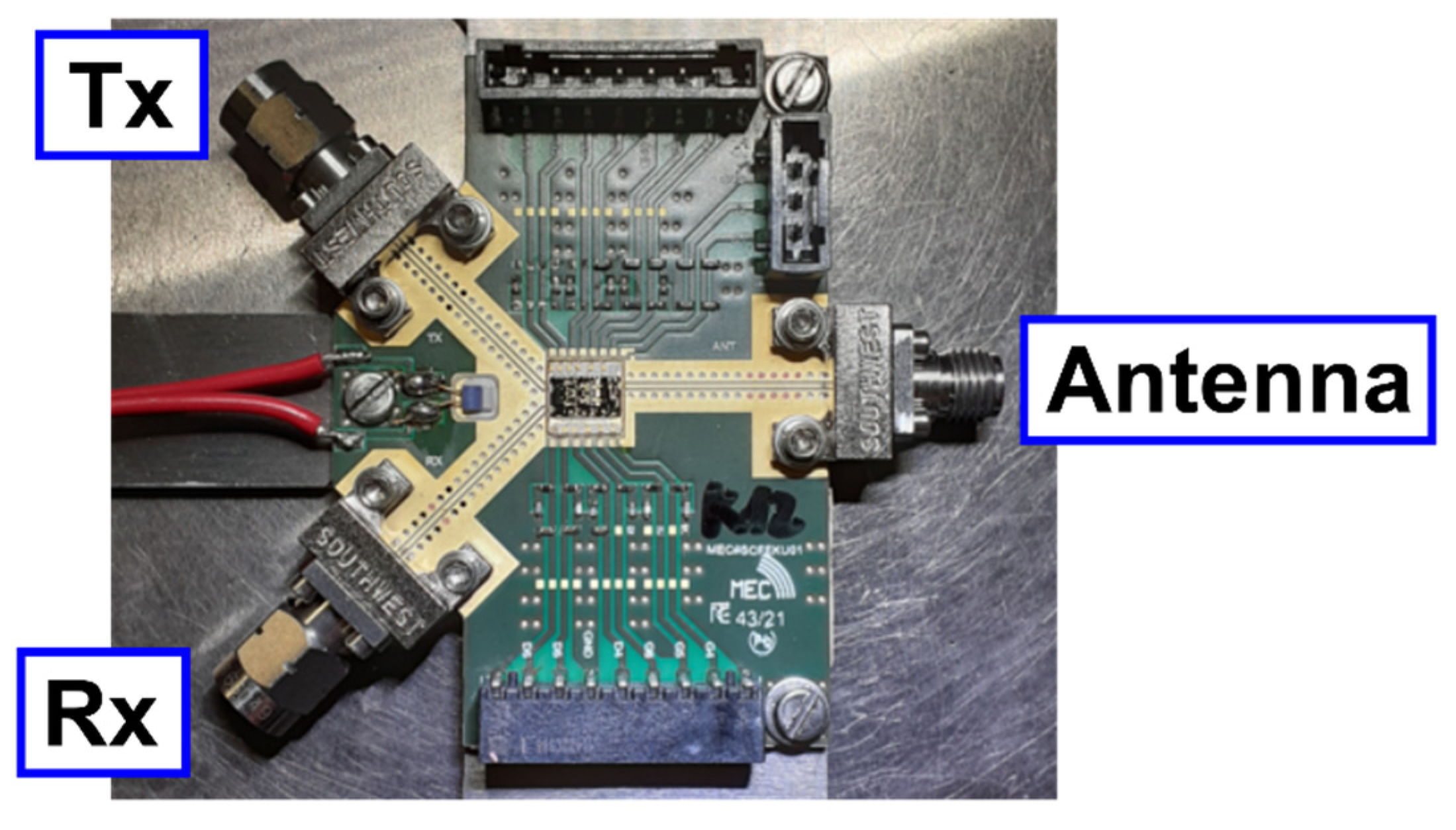
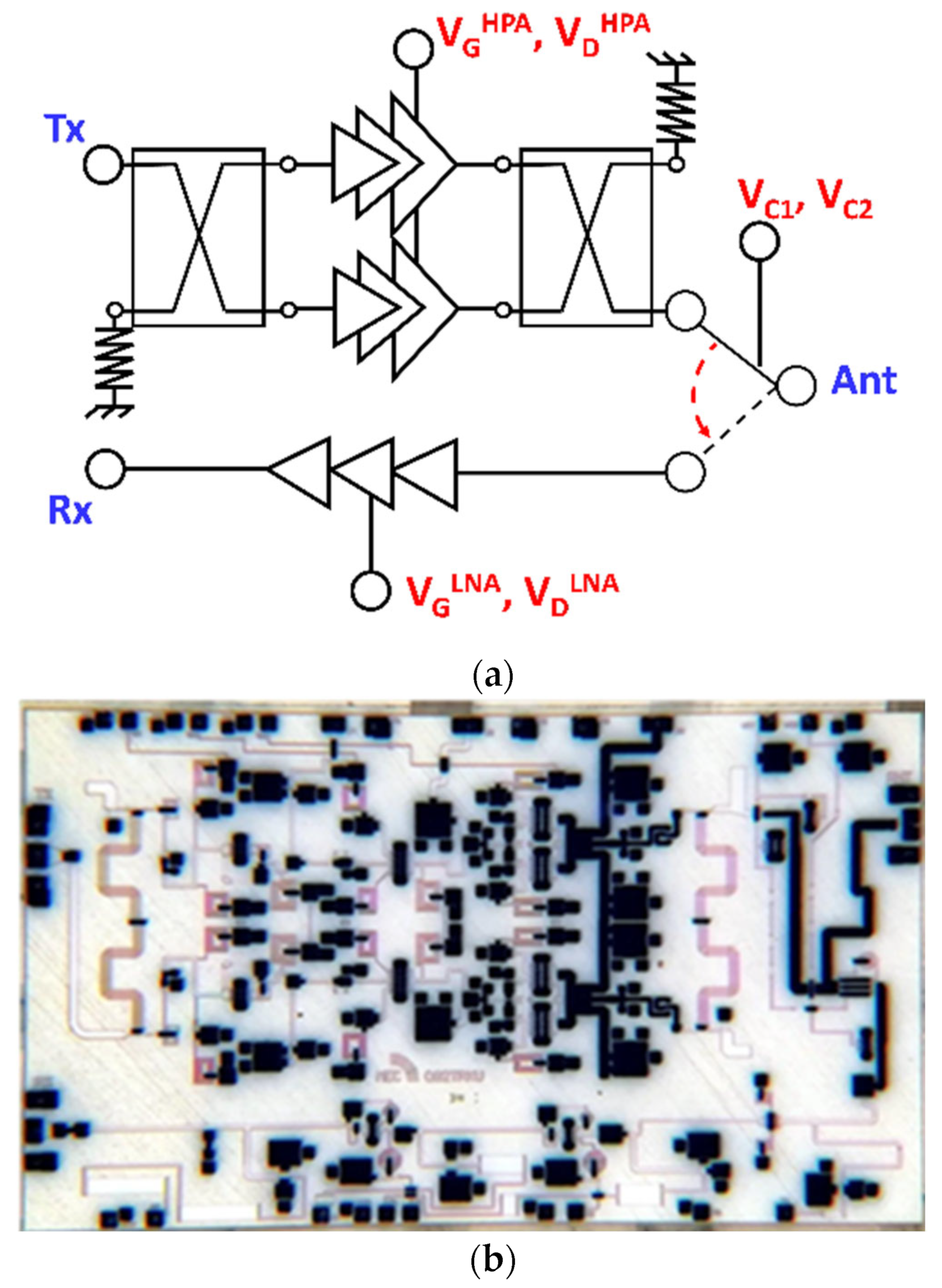
2.1. SCFE Architecture

The chosen architecture of the Ku-band SCFE is shown in Figure 1a. A three-stage HPA and a three-stage LNA are connected by a SPDT switching circuit controlling the antenna connection to the Tx and Rx ports, improving the isolation between the Tx and Rx paths. A balanced topology has been chosen for the HPA because it is useful in both guaranteeing a good Tx port matching and a good termination to the off arm of the switch during the Rx operation. This is quite important to avoid the reflective loading of the switched-off HPA upsetting the LNA performance during the Rx cycle.

2.2. MMIC Technology and Design

The GaN technology chosen for the MMIC SCFE design is the space-qualified GH15 HEMT process by UMS. By exploiting a gate length of 150 nm, it offers high power, low noise and switching devices, as well as the usual MMIC passives with two layers of metals. The chip photograph is shown in Figure 1b. A total die area of 20 mm2 has been occupied.
The balanced HPA of the Tx section uses 3.2 mm of active periphery in the output stage, 1.2 mm in the driver stage and 0.6 mm in the first stage. The HPA quadrature operation was obtained by exploiting a Lange coupler at the input and output ports. The final-stage periphery was chosen so that it was possible to target 10 W of output power to cope with the losses of the output combiner, Lange coupler and Tx path of the SPDT. The driver to final-stage periphery ratio was carefully selected to have enough drive margin available in the worst-case scenario, without sacrificing the overall efficiency. The HPA drain bias voltage and current density were set to 17.5 V and 80 mA/mm, respectively, after a careful tradeoff with operating temperature and antenna mismatch to make sure that the space de-rating maximum channel temperature of 160 °C was ensured at 100 °C of MMIC backside temperature and with an antenna VSWR of 2:1. The rest of the HPA design was focused on high-efficiency operation.
The LNA is a three-stage amplifier: the first stage was designed for the best noise and stability by exploiting negative inductive feedback on the source of the device; the second and third stages were designed for the best tradeoff between the noise figure, power gain and gain flatness using a conventional RLC feedback between the drain and the gate of the device. All three stages exploited the same 4 × 30-µm device, biased at 10 V and 100 mA/mm, which is the best drain-current density for noise. Resistive elements were exploited on the drain of each stage, appropriately tapered to guarantee the proper saturation of the LNA output power to 15 dBm in the presence of signals having very large amplitude. This was a fundamental design requirement of the LNA to protect the Rx path of the beamformer, which will eventually load the SCFE Rx port.
The SPDT circuit within the SCFE is a reflective design. The schematic is reported in Figure 2. The Tx arm of the SPDT makes use of two shunt devices of 4 × 40 µm and 4 × 100 µm, T1 and T2 in Figure 2, to sustain the output power of the HPA without entering in compression and to not increase the insertion loss. The Rx arm, instead, makes use of a 4 × 140-µm series device and a 4 × 50-µm shunt device, T3 and T4, respectively, in Figure 2. The series device was mandatory to increase the isolation during the Tx cycle, keeping the LNA safe when there is the highest power at the antenna. The chosen topology requires two complementary control voltages working at 0 V and −20 V in on and off conditions, respectively.

3. SCFE Experimental Characterization

Table 1 summarizes the bias and control signals applied to the SCFE depending on the Tx and Rx modes. A full characterization, at the ambient temperature of 25 °C, was carried out on the test fixture, shown in Figure 3, which was designed to accommodate the SCFE as well as launching lines to calibrate the measurements so that they include the effect of the actual bonding wire transitions to the external circuitry.
It is worth noting that the presence of trapping and thermal effects [12,13,14] makes the modeling and, consequently, the design of GaN MMICs extremely challenging with respect to other technologies such as gallium arsenide and silicon.

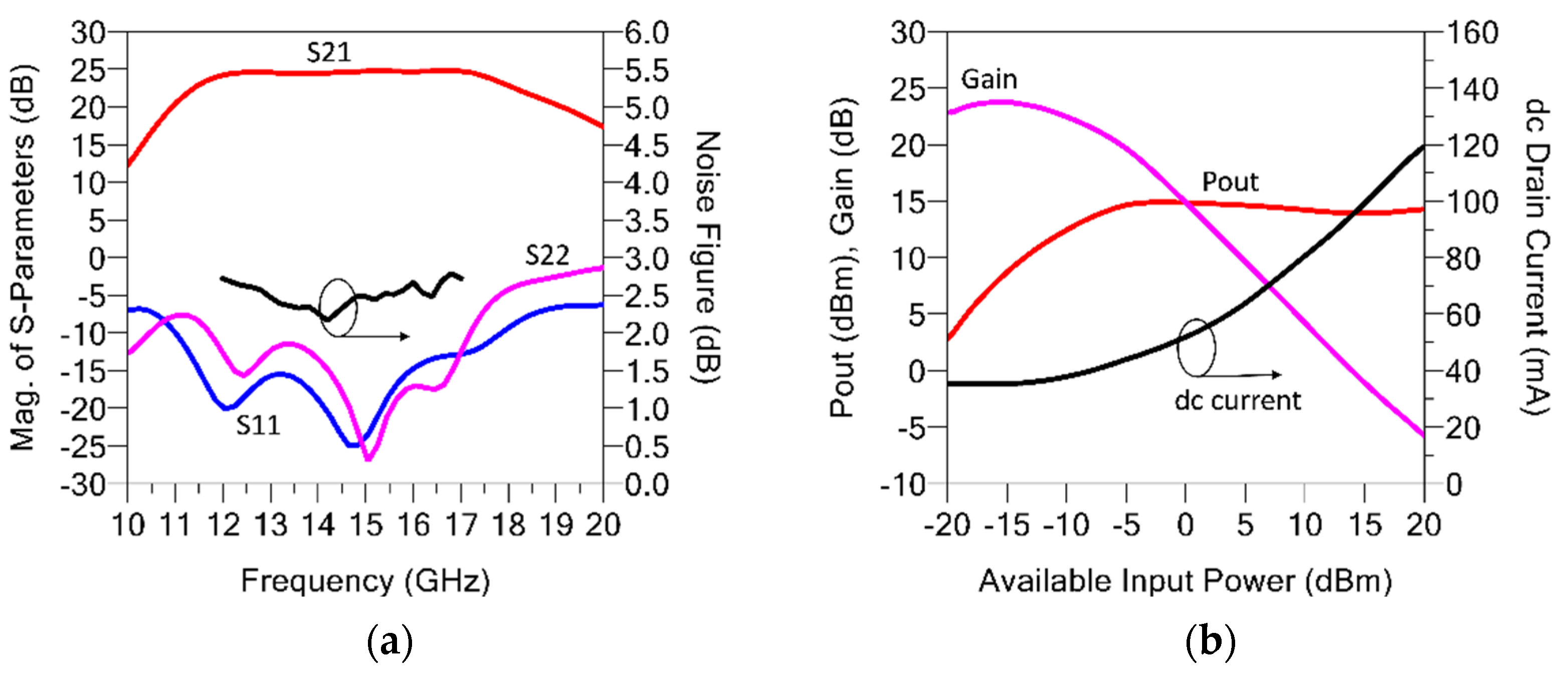
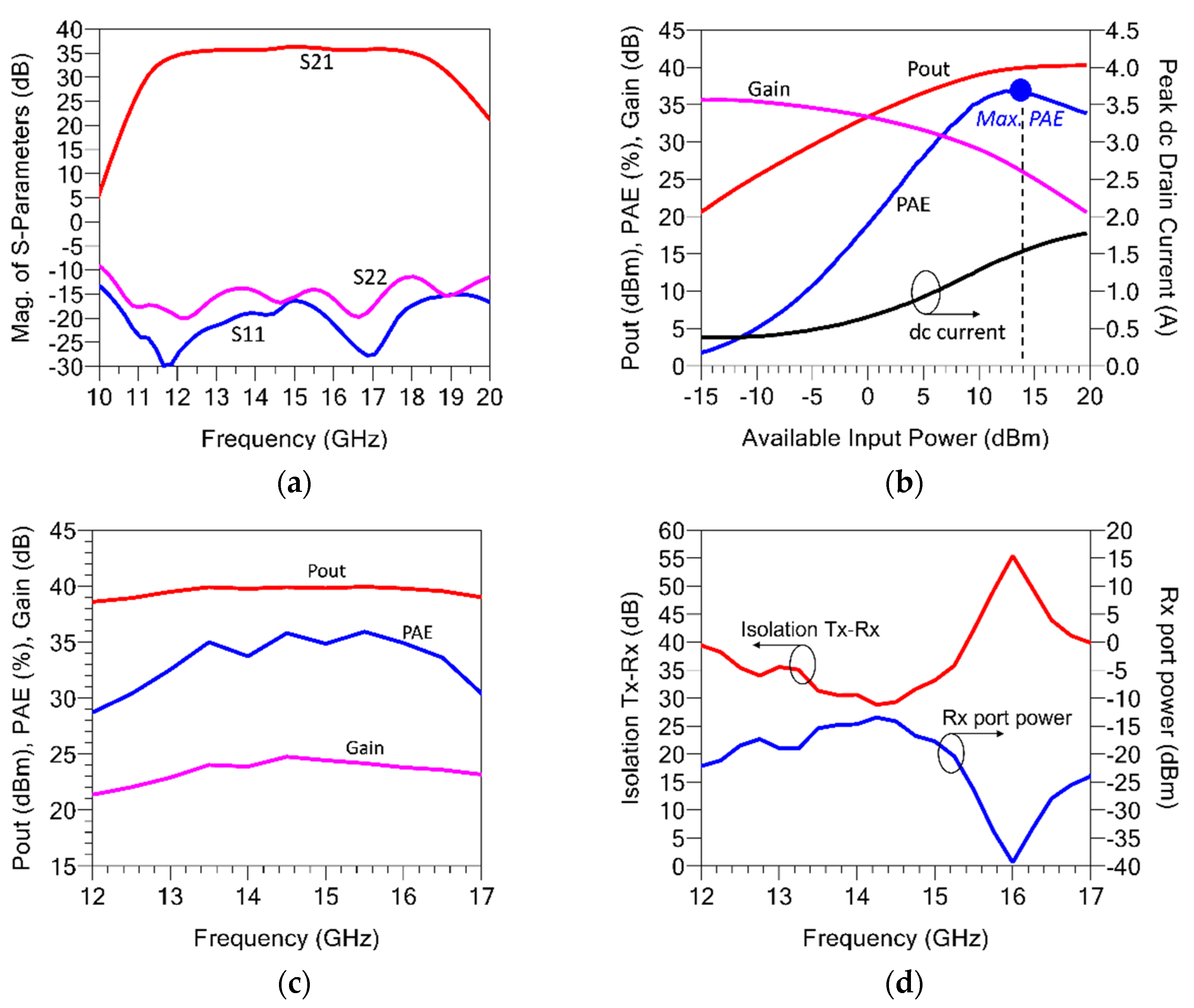
3.1. MMIC SCFE Measured Performance

Figure 4 shows the measured performance of the Ku-band SCFE in Tx mode. A linear gain of 35 dB with a good input and output return loss of 15 dB is reported. Let us consider the power added efficiency (PAE), calculated as
PAE = 100 P o u t P i n P D C
where P o u t is the output power, P i n is the input power and P D C is the DC-supplied power. The operating point at the maximum PAE is reached with 14 dBm of available input power. At this drive level, the SCFE gives the antenna port more than 39.5 dBm of output power with a PAE higher than 33%; such a performance is achieved in the frequency band from 13 GHz to 16 GHz. The corresponding operating gain is higher than 23 dB. The Tx–Rx port isolation is higher than 30 dB, and the leakage output power measured at the Rx port during the Tx mode is always lower than −15 dBm.
Figure 5 shows the measured performance of the Ku-band SCFE in the Rx mode. A linear gain of 25 dB with a good input and output return loss of 12 dB is reported for the receiving chain, in the frequency band from 12 to 17 GHz. In the same band, the measured noise figure, calculated as
NF = 10 log 10 ( S N R i S N R o )
where S N R i and S N R o are the input and output signal-to-noise ratios, respectively. It is always lower than 2.8 dB. The swept power measurements in Figure 5b show that up to 30 dB of gain compression can be reached with a limited output power of 15 dBm.
Table 2 compares the Ku-band SCFE presented in this work with similar SCFEs either found in the literature or as components-of-the-shelf. Since it is quite a new concept, it was not possible to limit the comparison with components in the same Ku-band, because none have been found either in the literature or as a commercial product. As can be seen, the SCFE concept has been applied to all of the main interesting frequency bands with performance ranging from a few watts to 40 watts of output power. Our design compares well in terms of performance to the two commercial products included in the comparison [15,16].

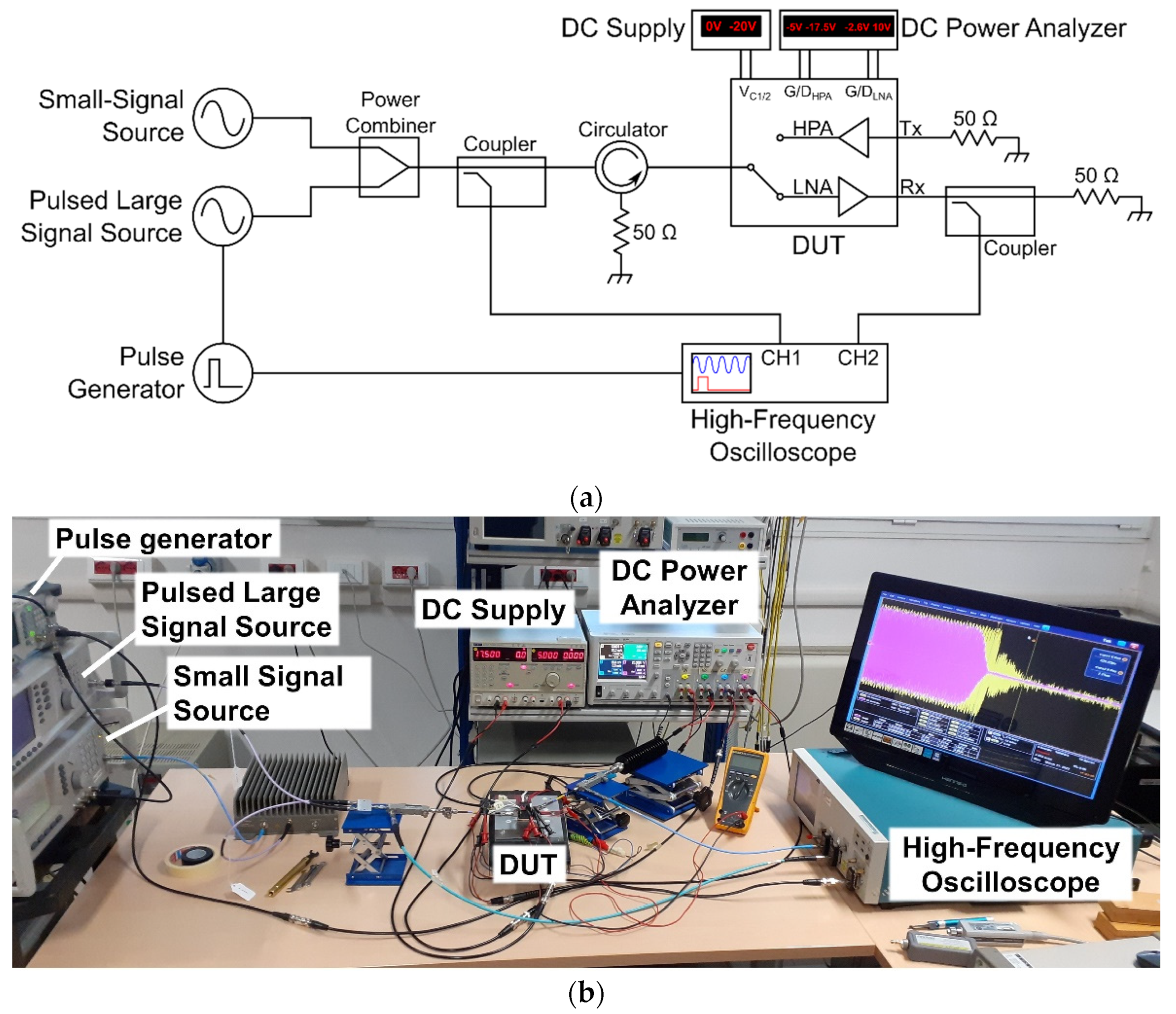
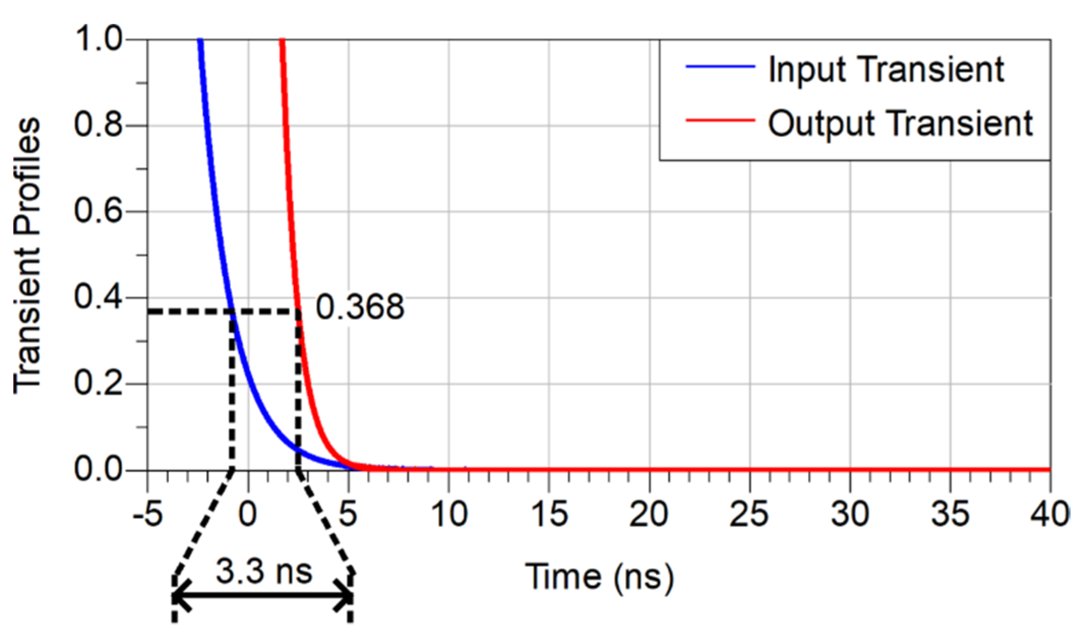
3.2. Receiver Recovery Time Test Setup

To characterize the recovery time of the receive section, we implemented the dedicated measurement setup that is reported in Figure 6. The RF signal is driven to the DUT by a small-signal source (Anritsu, USA, MG3694B, 2–40 GHz) combined with a pulsed large-signal source (Anritsu, USA, 68347C, 0.01–20 GHz), which is controlled by a pulse generator (Rigol, USA, AWG DG1032Z) to mimic a disturbance. In a real scenario, such large-signal disturbances may come from two different sources: either nearby modules in the antenna that reflect back signals having non-negligible energy content or external sources. The DC supply is used to properly set the DUT in the Rx mode. A DC power analyzer (Keysight, USA, N6705A) is adopted to provide the bias condition to both the HPA and LNA sections. The input and output signals on the Rx path are detected through two directional couplers (1–26 GHz, 10 dB) and measured using two channels of the high-frequency real-time oscilloscope (Tektronix, Germany, DPO75002SX, 33 GHz, 100 GSa/s) [17,18]. A circulator (7–18 GHz) connected to the input of the DUT improves the input matching of the system.
The waveform acquisition is synchronized with the interferer pulse by triggering the oscilloscope using the pulse generator as a reference.
The RF paths between the oscilloscope and the DUT have been preliminarily characterized by means of their S-parameters for evaluating insertion losses and delays, which allow the shift of the measurement reference plane from the oscilloscope channels to the DUT ports.

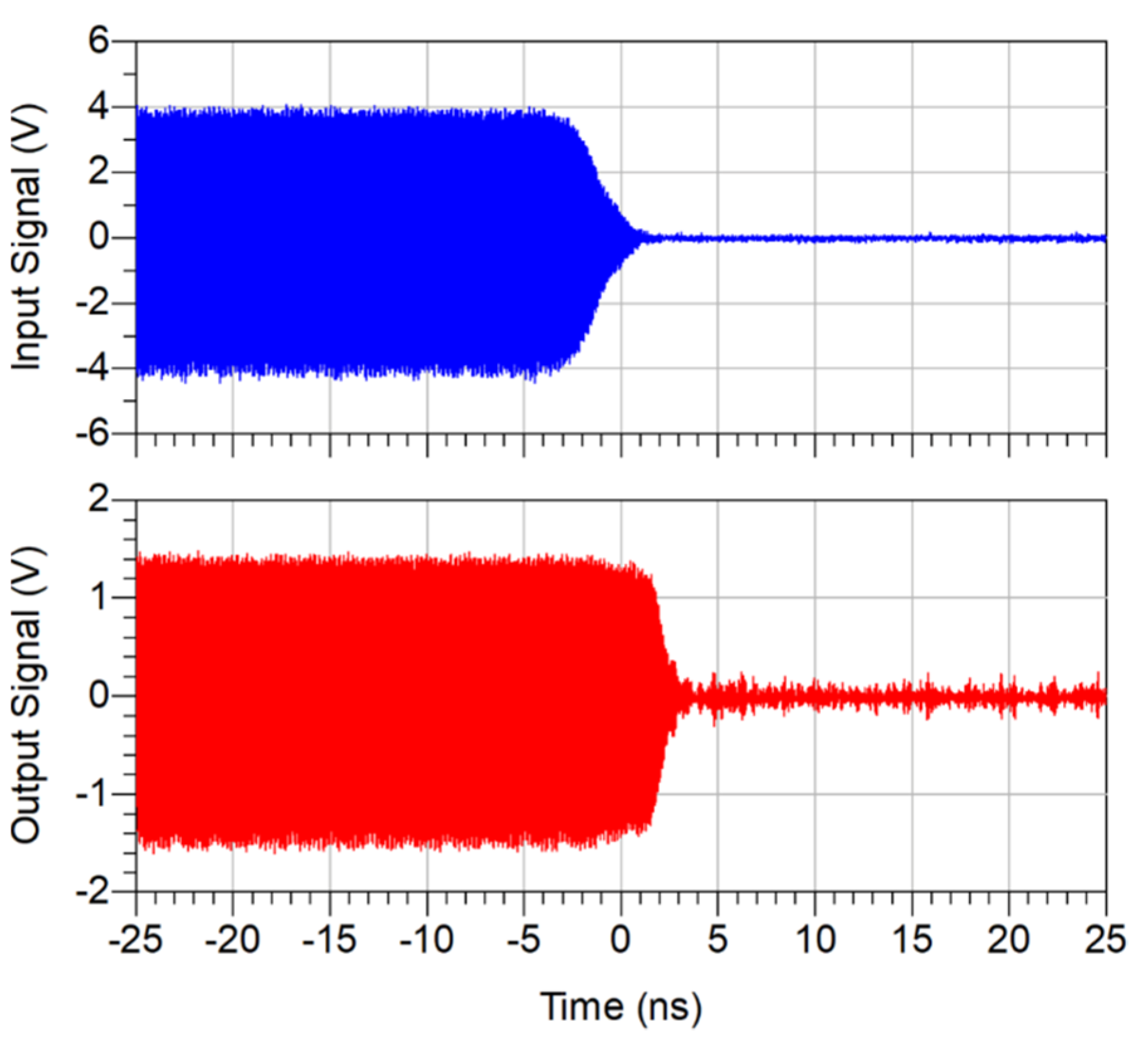
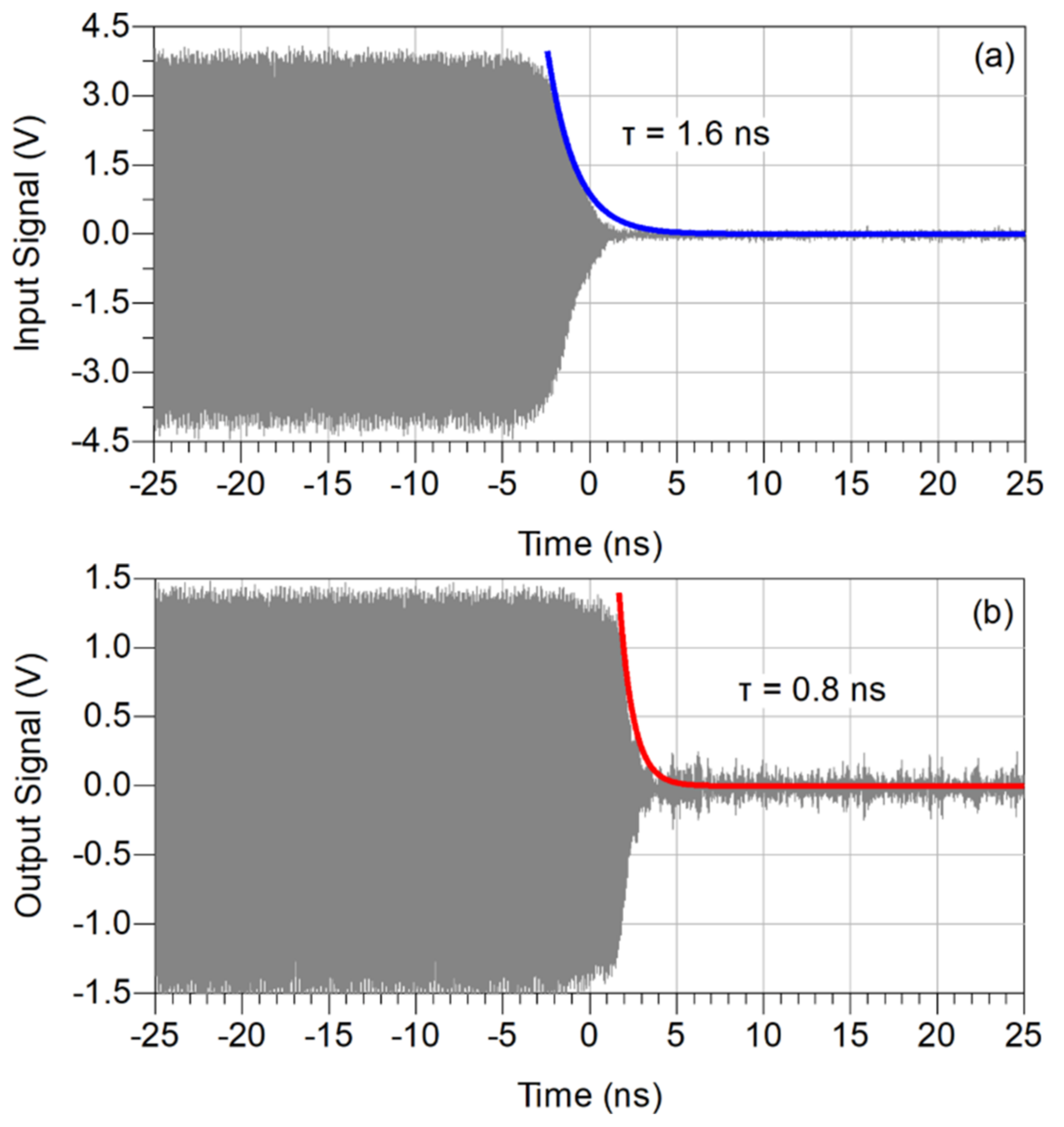
3.3. Receiver Recovery Time Experimental Results

To test the SCFE receiver section for the recovery time, a pulsed large-signal interferer of about 20 dBm was superimposed to the nominal input signal at the same frequency. A pulse repetition frequency of 100 kHz with a duty cycle of 50% was set up for the experiment. The measurement was carried out with an RF frequency of 13 GHz.
In Figure 7, we report the input and output measured signals, focusing on the transition between the saturated operation, due to the interferer pulse, and the return to the small-signal operation. Looking at the edges of the transient, the delay in the output response becomes clear when compared to the input transition. It is also interesting that, during the interferer pulse, the input signal has an amplitude considerably higher than the output signal, confirming the deeply saturated operation. To evaluate the recovery time, the transients have been approximated by a conventional exponential function:
x ( t ) = X 0 exp ( t t 0 τ ) ,
where X 0 , t 0 and τ are constants properly tuned to fit the transient edges.
The results of the fitting are shown in Figure 8, where the estimated time constants ( τ ) have also been reported. It is interesting that their values are not the same for the input and output transients, which can be ascribed to the nonlinear dynamic behavior of the active devices as well as to the circuit-matching networks.
By comparing the input and output transients, we can provide an estimation of the recovery time. In Figure 9, we report the optimized exponential functions normalized with respect to their amplitudes. We use the point at 36.8% (i.e., after one time constant from the beginning of the transient) as a reference point in both the transient edges. The recovery time can be assumed as the time difference between these points, which, in this case, results in 3.3 ns, which is an excellent performance for the SCFE.

4. Conclusions

A Ku-band SCFE operating in the frequency range between 12 GHz and 17 GHz has been presented. More than 39 dBm of output power with 30% PAE and 22 dB of power gain have been measured in Tx mode. A linear gain of 25 dB with less than 2.8 dB of noise figure characterizes the Rx chain. With a custom test setup, a recovery time lower than 4 ns has been measured in Rx mode in the presence of a large-signal interferer.

Author Contributions

Conceptualization, F.S. and D.R.; methodology, F.S., D.R., A.B. and S.D.; validation, G.B., L.C., A.B. and V.V.; investigation and data curation, D.R., V.V., G.B., A.B. and L.C.; writing—original draft preparation, D.R., G.B. and A.R.; writing—review and editing, D.R., G.B., A.B., S.D., L.C., V.V., A.R., F.S., E.C. and G.V.; supervision, A.R., D.R, F.S. and G.V.; funding acquisition, F.S. and A.R. All authors have read and agreed to the published version of the manuscript.

Funding

This activity was supported by the ESA Contract N. 4000130410/20/I-NS and by the Italian Ministry of University and Research (MUR) through the PRIN 2017 Project under Grant 2017FL8C9N.

Data Availability Statement

Not applicable.

Conflicts of Interest

The authors declare no conflict of interest.

References

  1. Masuda, S.; Yamada, M.; Kamada, Y.; Ohki, T.; Makiyama, K.; Okamoto, N.; Imanishi, K.; Kikkawa, T.; Shigematsu, H. GaN single-chip transceiver frontend MMIC for X-band applications. In Proceedings of the 2012 IEEE/MTT-S International Microwave Symposium Digest, Montreal, QC, Canada, 17–22 June 2012. [Google Scholar]
  2. Biondi, A.; D’Angelo, S.; Scappaviva, F.; Resca, D.; Monaco, V.A. Compact GaN MMIC T/R module front-end for X-band pulsed radar. In Proceedings of the 11th European Microwave Integrated Circuits Conference (EuMIC), London, UK, 3–4 October 2016. [Google Scholar]
  3. Schuh, P.; Sledzik, H.; Reber, R. GaN-based single-chip frontend for next-generation X-band AESA systems. Int. J. Microw. Wireless Technol. 2018, 10, 660–665. [Google Scholar] [CrossRef]
  4. van Heijningen, M.; de Hek, P.; Dourlens, C.; Fellon, P.; Adamiuk, G.; Ayllon, N.; van Vliet, F. C-band single-chip radar front-end in AlGaN/GaN technology. IEEE Trans. Microw. Theory Tech. 2017, 65, 4428–4437. [Google Scholar] [CrossRef]
  5. Giofrè, R.; Colangeli, S.; Ciccognani, W.; Costanzo, F.; Polli, G.; Salvucci, A.; Vittori, M.; Sotgia, M.; Cirillo, M.; Limiti, E. S-band GaN single-chip front end for active electronically scanned array with 40-W output power and 1.75-dB noise figure. IEEE Trans. Microw. Theory Tech. 2018, 66, 5696–5707. [Google Scholar] [CrossRef]
  6. Giofrè, R.; Ciccognani, W.; Colangeli, S.; Feudale, M.; Lanzieri, C.; Polli, G.; Salvucci, A.; Suriani, A.; Vittori, M.; Limiti, E. A C-Band GaN single chip front-end for SAR applications. In Proceedings of the 2020 IEEE Radio and Wireless Symposium (RWS), San Antonio, TX, USA, 26–29 January 2020. [Google Scholar]
  7. Pace, L.; Costanzo, F.; Longhi, P.E.; Ciccognani, W.; Colangeli, S.; Suriani, A.; Leblanc, R.; Limiti, E. Design of a Ka-Band Single-Chip Front-End based on a 100 nm GaN-on-Si technology. In Proceedings of the 2020 International Workshop on Integrated Nonlinear Microwave and Millimetre-Wave Circuits (INMMiC), Cardiff, UK, 16–17 July 2020; pp. 1–3. [Google Scholar]
  8. The European Space Agency—CRISTAL. Available online: https://www.esa.int/ESA_Multimedia/Images/2020/09/CRISTAL (accessed on 2 September 2022).
  9. Novaris, N.; Blount, P.; Trantanella, C. On the measurement of pulse recovery times in Gallium Nitride low noise amplifiers. In Proceedings of the 2017 47th European Microwave Conference (EuMC), Nuremberg, Germany, 10–12 October 2017; pp. 580–583. [Google Scholar]
  10. Liero, A.; Dewitz, M.; kuhn, S.; Chaturvedi, N.; Xu, J.; Rudolph, M. On the Recovery Time of Highly Robust Low-Noise Amplifiers. IEEE Trans. Microw. Theory Tech. 2010, 58, 781–787. [Google Scholar] [CrossRef]
  11. Axelsson, O.; Billström, N.; Rorsman, N.; Thorsell, M. Impact of Trapping Effects on the Recovery Time of GaN Based Low Noise Amplifiers. IEEE Microw. Wirel. Compon. Lett. 2016, 26, 31–33. [Google Scholar] [CrossRef]
  12. Nalli, A.; Raffo, A.; Avolio, G.; Vadalà, V.; Bosi, G.; Schreurs, D.M.M.-P.; Vannini, G. Extremely low-frequency measurements using an active bias tee. In Proceedings of the 2013 IEEE MTT-S International Microwave Symposium Digest (MTT), Seattle, WA, USA, 2–7 June 2013; pp. 1–4. [Google Scholar]
  13. Raffo, A.; Bosi, G.; Vadalà, V.; Vannini, G. Behavioral Modeling of GaN FETs: A Load-Line Approach. IEEE Trans. Microw. Theory Tech. 2014, 62, 73–82. [Google Scholar] [CrossRef]
  14. Santarelli, A.; di Giacomo, V.; Raffo, A.; Filicori, F.; Vannini, G.; Aubry, R.; Gaquière, C. Nonquasi-static large-signal model of GaN FETs through an equivalent voltage approach. Int. J. RF Microw. Comput. Eng. 2008, 18, 507–516. [Google Scholar] [CrossRef]
  15. QPM1002, Qorvo Product Datasheet. Available online: https://www.qorvo.com/products/p/QPM1002 (accessed on 15 July 2022).
  16. QPM2637, Qorvo Product Datasheet. Available online: https://www.qorvo.com/products/p/QPM2637 (accessed on 15 July 2022).
  17. Humphreys, D.A.; Raffo, A.; Bosi, G.; Vannini, G.; Schreurs, D.; Gebremicael, K.N.; Morris, K. Maximizing the benefit of existing equipment for nonlinear and communication measurements. In Proceedings of the 2016 87th ARFTG Microwave Measurement Conference (ARFTG), San Francisco, CA, USA, 27 May 2016. [Google Scholar]
  18. Avolio, G.; Raffo, A.; Jargon, J.; Hale, P.D.; Schreurs, D.M.M.-P.; Williams, D.F. Evaluation of Uncertainty in Temporal Waveforms of Microwave Transistors. IEEE Trans. Microw. Theory Tech. 2015, 63, 2353–2363. [Google Scholar] [CrossRef]
Figure 1. Ku-band SCFE architecture: (a) Schematic; (b) MMIC photograph.
Electronics 11 02998 g001
Figure 2. Schematic of the SPDT circuit.
Electronics 11 02998 g002
Figure 3. Test fixture for the characterization of the prototype of the SCFE.
Electronics 11 02998 g003
Figure 4. Ku-band SCFE-measured performance in Tx mode. (a) Measured S-parameters; (b) output power, PAE and gain as a function of the available input power; (c) output power, PAE and gain and (d) Tx–Rx port isolation and Rx port leakage output power at fixed available power Pavs = 14 dBm as a function of frequency. Bias and control voltages are set according to Table 1.
Electronics 11 02998 g004
Figure 5. Ku-band SCFE measured performance in Rx mode. (a) Measured S-parameters and noise figure; (b) output power, gain and DC drain current as a function of the available input power (b). Bias and control voltages are set according to Table 1.
Electronics 11 02998 g005
Figure 6. Test setup for the characterization of the Rx recovery time. (a) Block diagram; (b) implemented setup.
Electronics 11 02998 g006
Figure 7. Input and output measured signals for the characterization of the Rx recovery time at 13 GHz.
Electronics 11 02998 g007
Figure 8. Approximation of the signal edges with an exponential function. (a) Input signal; (b) output signal.
Electronics 11 02998 g008
Figure 9. Comparison between the normalized input and output transients and evaluation of the recovery time.
Electronics 11 02998 g009
Table 1. SCFE bias requirements in the different modes.
SymbolTx ModeRx ModeUnit
V D H P A 17.517.5V
I D Q H P A 4000mA
V G H P A −2.75−5V
HPA modePulsedPulsed
Pulse width150/µs
Duty cycle40/%
V D L N A 1010V
I D Q L N A 360mA
V G L N A −2.6−7V
V C 1 , V C 2 −20, 00, −20V
Table 2. Comparison between the presented SCFE and other state-of-the-art SCFEs.
ReferenceTx ModeRx ModeChip Area
(mm2)
Frequency
(GHz)
Pout
(dBm)
PAE
(%)
Gain
(dB)
Tx–Rx Iso
(dB)
NF
(dB)
Gain
(dB)
[1]10.538.2301930 *3 **18 **11.88
[2]8.6–11.2392513402.5159.00
[3]7.7–12.241.22426-3.21412.96
[4]5.2–5.6463618.5-2.431.536.00
[5]13% in
S-band
464235-1.753049.00
[6]5.25–5.75463036-3.23549.00
[7]35–36.534 #25 #20 #-3.15 #31.5 #12.96 #
[15]8.5–10.534.53225182.224.525.00 ##
[16]9–10.5363823502.72125.00 ##
This work13–1639.53323302.82519.96
* SPDT only, ** LNA only, # simulation only, ## packaged product.
Publisher’s Note: MDPI stays neutral with regard to jurisdictional claims in published maps and institutional affiliations.

