1. Introduction
A photoconductive semiconductor switch is an electrical switch whose conductivity can be modulated by light illumination of a suitable wavelength. Such semiconductor switches, especially in the high voltage context, are an attractive proposition for various applications such as imaging and radar systems, biological medicine, solid-state high-power microwave (HPM) sources, and next-generation accelerators [
1,
2,
3,
4]. Other applications include: (i) Photoconductive sampling for testing of high-speed integrated electronic circuits. (ii) The generation of terahertz pulses. (iii) The generation of microwaves and millimeter waves via direct current (DC) to radio-frequency (RF) conversion. (iv) Photodetectors for high-speed optical fiber communications. (v) Quick and efficient analog-to-digital converters.
Historically, Auston was the first to suggest and probe such photoconductive applications [
5]. Many such devices utilize light absorption of energy greater than their bandgap [
6,
7,
8,
9,
10,
11], the so-called extrinsic mode, using materials such as GaAs and low-temperature grown gallium arsenide (LT-GaAs), InP, GaN, SiC materials, silicon on sapphire, etc. [
12,
13,
14,
15,
16,
17,
18,
19]. Furthermore, sub-bandgap radiation has also been used in some cases (the intrinsic mode) for materials having well-defined, intentional energy states in the forbidden zone [
20,
21]. In order to lower the switch recovery time (determined by the lifetime of photoexcited carriers), one typically uses low-temperature growth (often followed by rapid thermal annealing) with GaAs material being a typical example, some impurity doping (e.g., chromium in GaAs), or neutron bombardment for producing crystal defects to reduce carrier lifetime. Apart from the recovery time, other important criteria are the electrical breakdown resistance, dark resistivity, and bandgap energy.
Compared to other high-power switches (e.g., spark gaps, insulated gate bipolar transistors, and thyristors), PCSS devices have unique advantages including ultrafast switching, reliable operation, negligible jitter time, and the ability of solid-state microwave generation [
22,
23,
24]. The PCSS devices can operate in either the linear or nonlinear modes. In the linear mode, the photoconductivity is proportional to the incident laser/photon power, while in the nonlinear mode, field-dependent avalanche processes are initiated for high gain [
25], though device instability can become an issue [
26,
27].
While all such devices are usually fabricated based on the metal–semiconductor–metal (MSM) structure, it may be mentioned for completeness that there are broad designs of photoconductive switches, namely: (i) Vertical bulk devices that could be several millimeters or even centimeters long and have electrical contacts at the two opposite, end faces. These are typically used for switching high voltages of 100 kV or higher. (ii) Lateral devices with a small gap in a microstrip. The gap can be straight or interdigitated (for increased perimeter) and has a width between a few microns and tens of microns; for low-power applications with high speeds. (iii) Sliding contact devices are another variation that provide for the highest speed, wherein a point between the two parallel strips of a coplanar stripline is illuminated.
The recent rise in need for components that can operate in harsh environments with small footprints has generated renewed interest in solid-state amplifiers over the previously used traveling wave tubes (TWT) [
28,
29]. Solid-state devices have shown the ability to withstand harsh environments, while being able to generate significantly less jitter and faster rise times [
30,
31]. Previously, semi-insulating GaAs (SI-GaAs) material had typically been popular for use in the PCSS spectrum [
32]. However, GaN with its ability to operate at high-power densities and currents, coupled with the significantly higher breakdown field as compared to GaAs has made it more appealing for a wide variety of applications such as directed energy systems and particle accelerators. GaN also has a significantly higher breakdown field thresholds and superior thermal conductivities as compared to GaAs. Furthermore, in comparisons GaAs, it has superior Baliga- and Johnson-figures of merit [
33] which are important for high speed and high power applications.
The scope of this work is to further probe of the potential applications of GaN PCSS devices for pulse compression, which could then lead to increased frequency operation. Previous work has been performed to show that when operating in the negative differential mobility (NDM) regime which is present in the GaN field versus velocity characteristic, one can achieve output current pulses whose temporal widths match or are lower than the input laser pulse [
34]. Similar trends have been shown experimentally in materials such as GaAs with pulse compression of up to 66% based on a similar negative differential mobility material property [
35,
36]. The present work focuses on other variables such as the density and location of the photoexcitation within the device to assess their contributions to pulse compression in GaN PCSS devices.
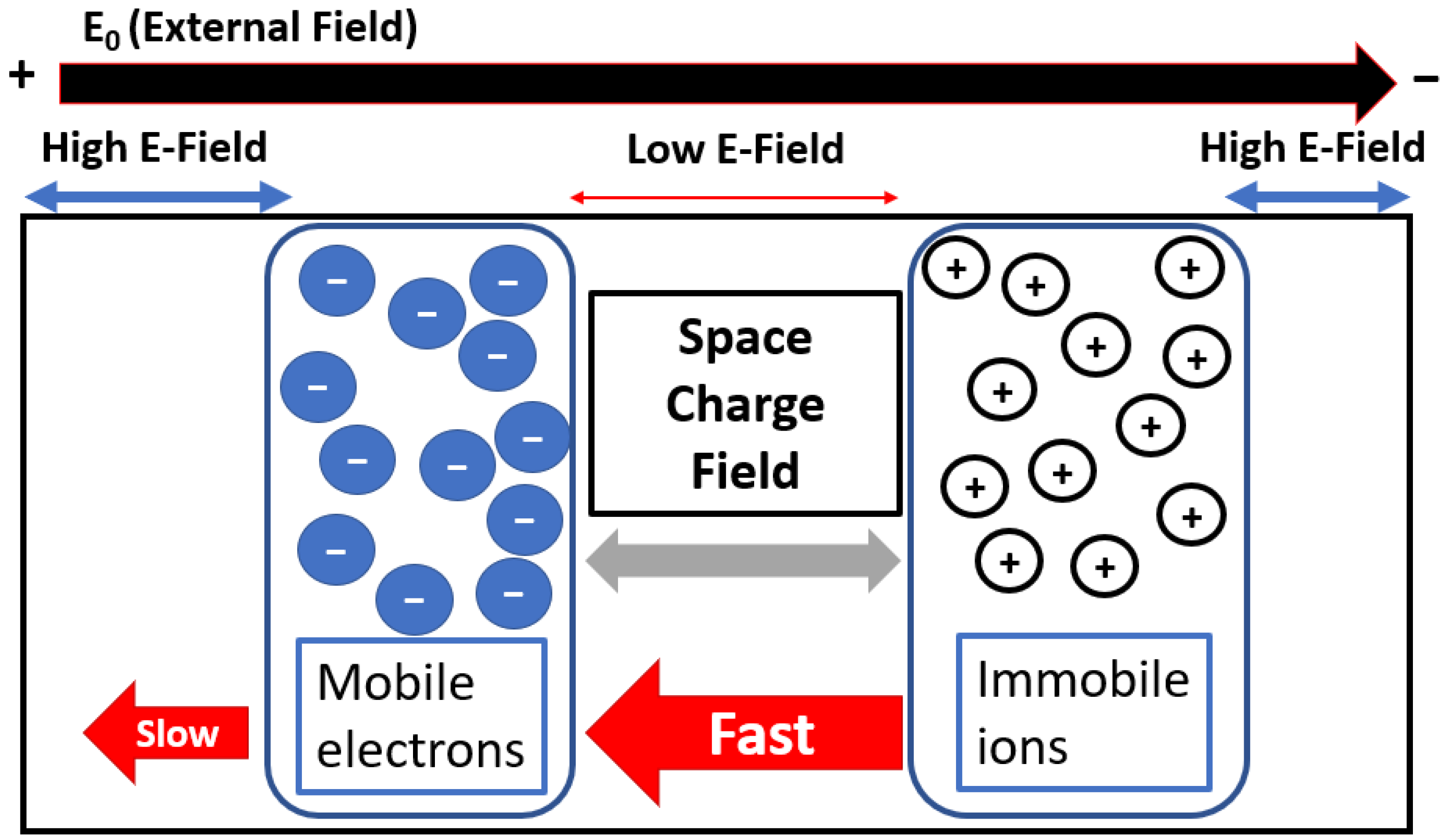
Previous attempts at pulse compression PCSS devices have focused on utilizing biasing fields within the NDM regime of the device. However, this work focuses on potential methods of amplifying the benefits through modulation of the space charge fields inside the device. The NDM assisted pulse compression is based on using the internal space-charge to alter the spatial field profiles. For instance, some parts of the photogenerated electron swarm in one region (say the leading edge) would effectively experience a different field from those in the swarm at a different location (say the trailing edge). A simple schematic of this differential field creation as the result of space-charge effects is given in
Figure 1. Due to internal polarization, the field at the central region (between the moving electron swarm on the left and the ions to the right) would be lower, while higher field values would exist at the left- and right-most regions. If the device were biased at the cusp of the NDM region, the electron velocities in the leading edge of the swarm would be lower (due to the higher local fields) than at the trailing edge. This would then effectively result in pulse compression. Additionally, as the compression of the electron cloud is a transient process, a potential longer distance of transit could compress the cloud further. Since the outcome depends on spatial field modulation, and hence, the level of space-charge, changes in its density through variations in the incident laser intensity could be used to alter the compression. One would expect greater pulse compression benefits at larger photoexcitation carrier densities. It may be mentioned that in the present simulations, the applied bias was deliberately not set at very high levels beyond the point of maximum electron drift velocity, to avoid any possible impact ionization and the resulting production of slower moving holes.
Here, quantitative predictions pertaining to the FWHM for a carbon-doped GaN PCSS device are presented.
Section 2 briefly describes the device structure used and provides details of the computational methods for the simulations for treating electronic transport in a many-valley model for GaN that includes electron-phonon scattering, Pauli exclusion, and the dynamic field evolution for self-consistency. The fast multipole method was used to account for the many-body contributions to the electrostatic fields.
Section 3 discusses photocurrent results, FWHM of current waveforms, valley occupation at different applied biases and times, and spatial distributions of particles obtained over the course of various simulation runs. Discussion of results and physical reasoning behind predicted behaviors are provided in the section as well, with a focus on pulse compression.
2. Modeling Methodology
The PCSS device used for our simulation analysis was reverse biased carbon-doped wurtzite GaN p-i-n diode structure. This provides for a near uniform starting electric field, reduces carrier injection from the contacts, and provides a central C-region for sub-bandgap absorption over a compact zone. The carbon-doped GaN material is known to have energy levels at about 0.89 eV from the valence band [
37,
38,
39], which would allow photons at about 405 nm (available from laser diodes, or frequency doubled from a Ti:Sapphire lasers) to photogenerate electrons from these levels associated with carbon doping to the conduction band. The use of a laser with sub-bandgap energy would only excite electrons from the traps to the conduction band in the carbon-doped GaN section, while having negligible carrier generation throughout the rest of the p-i-n device, and avoiding any hole creation. The p-i-n GaN structure was taken to be 12 μm thick, with other parameters in line with a previous report [
34]. The carbon-doped GaN was assumed to be 1 μm thick with each transverse dimension taken to be 50 μm. It was the target for external illumination by a Gaussian intensity profile
I(z), taken to have the form:
I(z) = I(t) exp(−2z2/w02) and width
w0 of 100 nm. The laser pulse intensity
I(t) was assumed to have the usual squared secant-hyperbolic shape, and thus:
I(t) = I0 sech2(t/τ), with
τ the pulse width, which is typical of ultrashort laser pulses [
40]. In the present simulation, the presence of holes was justifiably neglected, since the sub-bandgap irradiation would only generate electrons from the filled traps near the valence band in the carbon doped section.
The utilization of the NDM regime requires biasing the PCSS device at a field that is just around the maximum point on the drift-velocity curve. For GaN, this field has been predicted to be around 180–200 kV/cm [
34,
41,
42]. When modeling high densities of particles, it becomes necessary to utilize a computational method to effectively manage larger densities without increasing the computational weighting significantly. Here, 5000 macroparticles were used for the simulations. Each of these particles are assigned a weightage based on the number of electrons they should represent. This weightage directly effects the charge of the electron and allows one to model high densities of electrons without encumbering a heavy computational burden, as might have occurred upon scaling the particle populations.
When modeling the dynamics of charge carriers in PCSS devices, particular care must be taken to ensure that complex material specific behaviors such as scattering processes, long distance electrostatic forces, and adequate accounting of state occupancy with regard to the Pauli Exclusion Principle in the individual valleys within a multi-valley transport model, are all implemented. This section will briefly touch upon these aspects and the transport modeling methodology used for charge carrier transport in the simulation. A more rigorous account of this methodology can be obtained in a previous work [
34].
Electron transport in the bulk semiconductor material was modeled by utilizing a kinetic ensemble Monte Carlo (MC) method. This method was chosen for its repeated and widely accepted usage in the literature [
43], as well as its highly accurate handling of material specific processes and properties. It also does not require fitting transport parameters (such as mobilities or diffusion coefficients), which are necessary in other continuum analyses for electronic devices. Furthermore, temperature, density, size- and field-dependent variations can naturally be obtained. A three-valley model was used for the Monte Carlo simulations. Parameters relating to the GaN band structure such as the effective mass, wavevector-dependent energies, etc., were obtained based on calculations using the SIESTA code [
44,
45] which utilizes density functional theory (DFT). The current simulations used the primary (lowest energy)
Г1 valley, as well as the secondary and tertiary
L-M and
Г2 valleys, respectively. However, parameters such as the intervalley separation energy or even the fundamental bandgap as predicted by DFT are known to deviate substantially from actual experimental data. Hence, here, we have used well known values reported in the literature for most of the parameters. These values are discussed later in the context of
Table 1. However, the nonparabolicity factors were estimated from the momentum-dependent energies predicted by the SIESTA code.
Scattering processes were managed within the kinetic Monte Carlo approach. An ensemble of particles was created over time at different positions within the carbon-doped GaN to mimic the photogeneration process. Their trajectories were then calculated, which consisted of a series of free-flight-times, interrupted by instantaneous collisions with phonons and lattice impurities. Collision times were determined based on the energy of the particle at the different instants. The model included interactions with acoustic modes via the deformation potential, in addition to polar optical phonon interactions, and intervalley deformation potential scattering [
34]. The piezoelectric scattering was excluded since it is known to be negligible at room temperatures with negligible influence on high field transport [
46]. As is known, the transfer between one valley and another tends to lead to a change in the effective mass of electrons. In this work, the effective mass of the primary valley is obtained based on the nonparabolicity factor found in the bandstructure calculation. For the primary valley, this resulted in an effective mass of 0.2m0 where m0 is the rest mass of the electron. Effective masses for the secondary and tertiary valleys were found to be 0.4m0 and 0.6m0, respectively. A brief list of values pertinent to the present simulations is given in
Table 1.
While implementing the scattering of electrons with the phonons based on various interactions, the Pauli Exclusion Principle was taken into account, with a numerical implementation based on the work by Lugli and Ferry [
48]. Considerations of Pauli Exclusion (PE) become necessary when simulating devices at high electron densities, as is the case in the present calculations. For implementing PE, the normalized distribution function
fc at the discretized
k-space corresponding to the chosen final state is compared to a random number
r. between zero and one. For
r >
fc, the Monte Carlo transition to the chosen final state was accepted only for
r >
fc, or else was treated as a self-scattering event. A larger occurrence of such PE related scattering restrictions would tend to increase the average electron ensemble velocity. In addition, such scattering restrictions would also tend to keep electrons in the lowest valley. Implementations of the Pauli Exclusion Principle have shown to maintain higher average electron energies [
34,
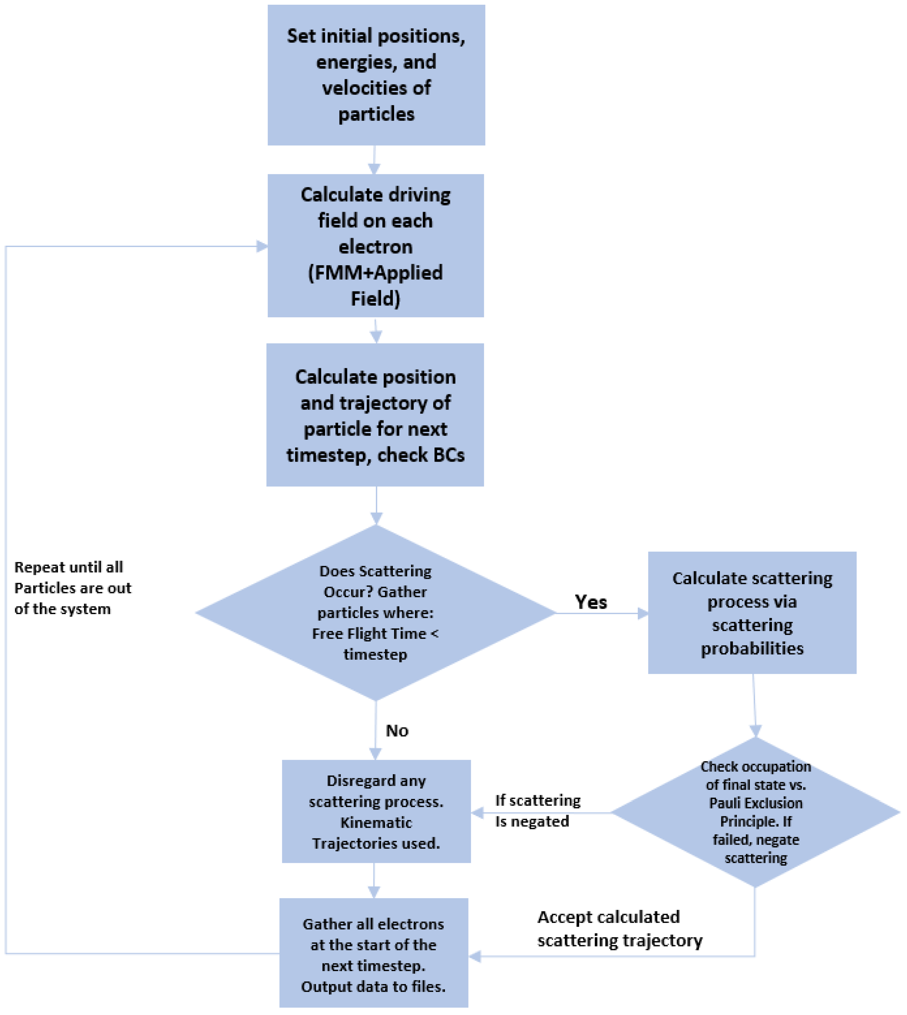
48], with the effect having a density dependence. A flowchart containing the full outline of the simulation is shown in
Figure 2. As outlined in the flowchart, basically, the carriers are assumed to be created in the C-doped GaN region by the externally applied laser. The motion of the photogenerated electrons was then followed based on Newtonian mechanics, with electron free-flights interrupted by scattering. As a result of the collision, the energy and momentum of the parties was changed based on the type of scattering event the electron was deemed to have undergone. The choice of scattering was based on a selection from a set of scattering processes germane to GaN material (e.g., acoustic phonon interaction, optical phonon absorption or emission, intervalley deformation potential transfer, etc.), with weightage given to their relative probability of occurrence at any given energy. This method is typical of all Monte Carlo transport simulations. The Pauli exclusion principle was taken into account at each scattering event to determine if a chosen collision would indeed be permitted based on the availability of an empty final state. Finally, changes in the internal fields, based on the evolutionary movements of the spatially distributed charge were taken into account via the Fast Multipole Method (FMM).
Finally, long-distance electrostatic forces need to be calculated for proper handling of the effect of the net effective driving forces and fields on the electron population. In the past, methods that combine direct calculations of particle-to-particle forces, as well as mesh forces, had been studied with the particle-particle-particle-mesh (P
3M) algorithm proposed by Hockney and Eastwood [
49]. This method works well for uniformly distributed ensembles of particle and is sufficient when the necessary precision is low. However, for higher precision algorithms that still maintain lower computational weightage at high carrier densities, the fast multipole method (FMM), originally devised by Rokhlin [
50] and improved on by Greengard [
51], is a better option for inclusion of the electrostatic calculations. An FMM solver was used in this work which is part of the Scalable Fast Coulomb Solver (ScaFaCoS) package. This was selected for its high accuracy and best-case O(N) scalability. The inclusion of a highly accurate solver for electrostatic forces is necessary to obtain the N-body forces on individual electrons inside of the electron cloud as well as interactions with the ion cloud. Results of the pairing of this method with the kinematic Monte Carlo are presented in the next section.
3. Results and Discussion
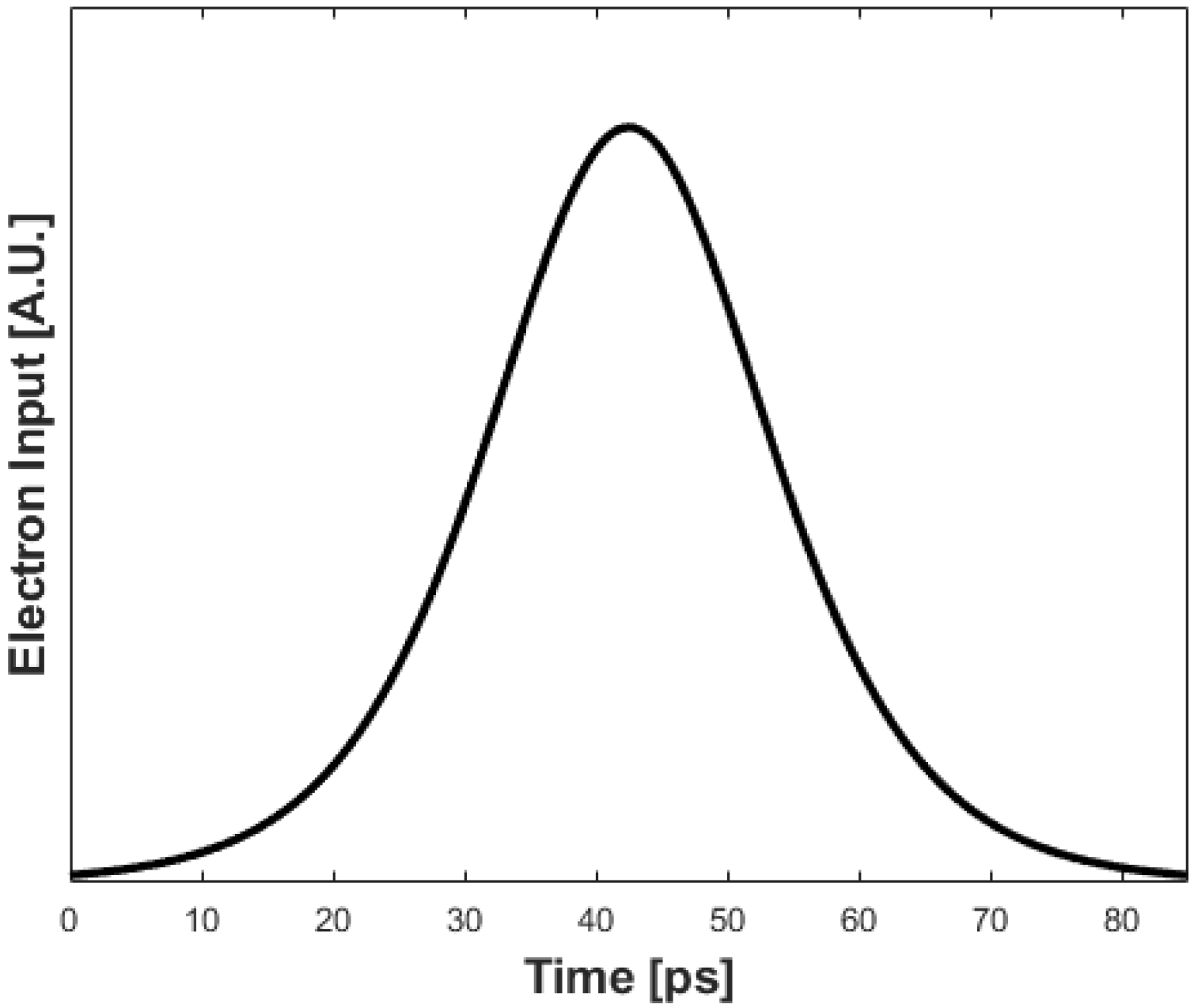
Simulations are conducted assuming a 25 ps laser with a hyperbolic secant square shape as shown in
Figure 3. For this shape, about 50% of the photogenerated electrons are created in the carbon-doped region within 41 ps. Thus, effects such as screening, Pauli Exclusion-based reductions in scattering due to final state occupancy, polarization contributions to the local field leading to pulse compression, etc., would likely begin playing a strong role around these times. Since a maximum of 5000 particles were used for the simulations from consideration of computational speed, the weightage of the super-particles was continually assigned and updated during the photogeneration process. In this simulation, and all other simulations described here, the average applied field was 200 kV/cm.
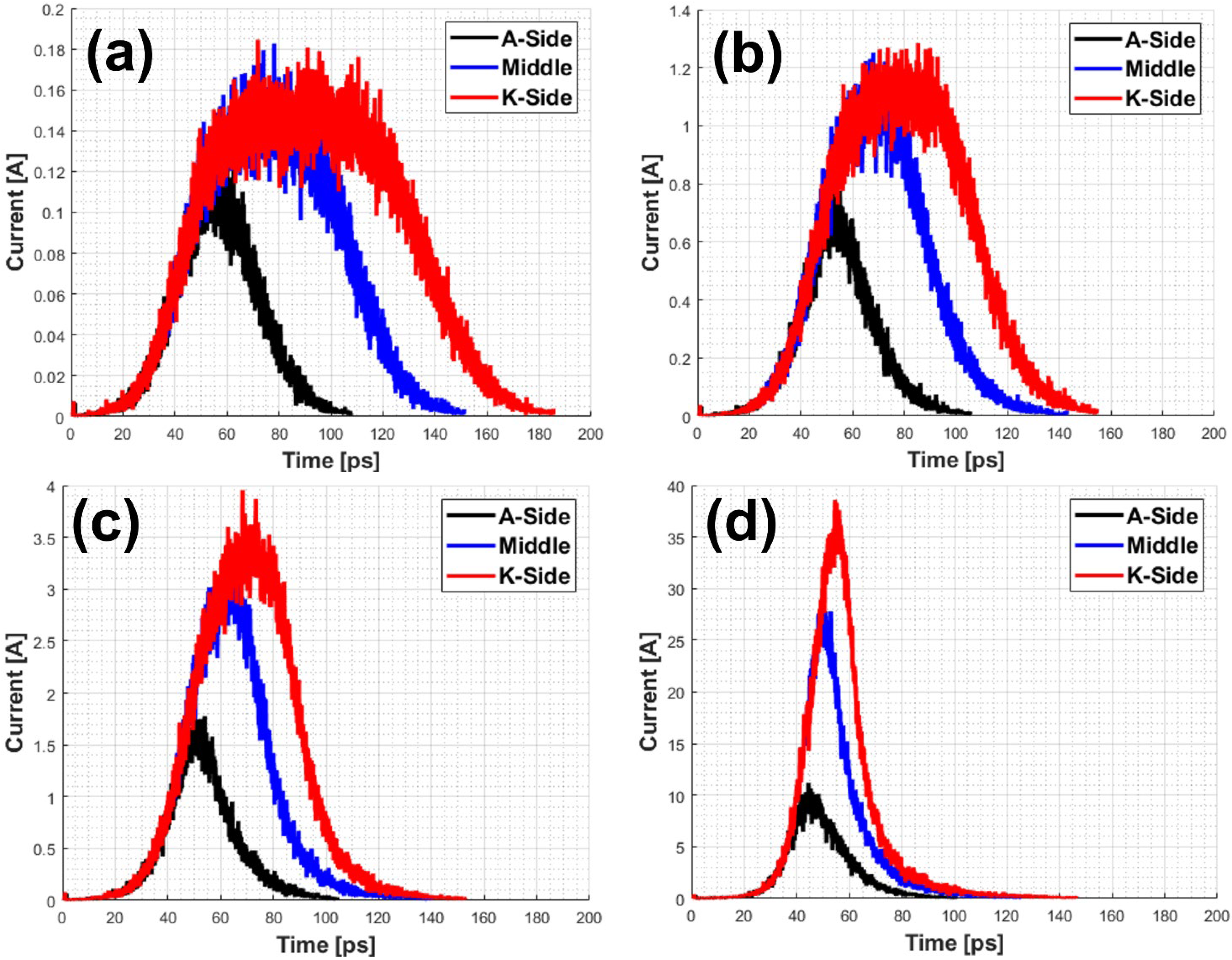
Among the various variables, the photogenerated carrier density and its evolution was of special interest and was carefully explored in this work. Different simulation runs were performed, each with a different photon intensity to vary the density of photogenerated carriers. The aim was to probe and quantify any changes in terms of the overall current response or pulse compression brought about due to density variations. The second variable that was altered to probe any changes was the position of the photoexcitation region. For example, the carbon-doped layer was taken to lie either at the center of the 12 μm thick PCSS, or towards the anode side, or towards the cathode end. These changes in location were aimed to study possible effects of transit time and transport distance on the pulse compression outcomes. It may qualitatively be expected that a longer transport time would provide more time for trailing electrons to catch up if they were moving at higher speeds, and thus yield a shorter photocurrent pulse.
Figure 4a–d displays the results of our study with these variations. Three different locations of the carbon-doped layer on the 12 μm long PCSS p-i-n structure were used. One was at the center, a second case had the intrinsic region nearer the anode at a 3 μm distance from it, while the third case was nearer the cathode placed 3 μm away from that electrode. For each of the three carbon-doped intrinsic layer locations, four different excitation densities of 10
22 m
−3 in
Figure 4a, 5 × 10
22 m
−3 in
Figure 4b, 10
23 m
−3 in
Figure 4c, and 5 × 10
23 m
−3 in
Figure 4d were used to study the effects of stronger illumination on pulse compression. The average applied field was taken to be 200 kV/cm. In
Figure 4, the A-side denotes an anode-side placement of the intrinsic layer, the K-side corresponds to the cathode side case, while the third was at the center location. As seen from
Figure 4a–d, the photocurrent initiation is the slowest for the K-side case, which is expected since the traversal distance to the anode collector is the largest. Similarly, the time for current decay in this case is also the longest. Photocurrent with the anode-side illumination starts the soonest, and also ends the earliest of the three cases. Furthermore, the effect of the carbon-layer region location on the current shape is seen to be less pronounced as the densities of the excited electron cloud are increased. At the highest density (5 × 10
23 m
−3) shown in
Figure 4d, the current waveforms are almost identical regardless of the location of the excited cloud, with only a slight offset in the waveforms due to the varying location that is still present. The increasing electron density not only has the effect of space-charge enhancement and accompanying pulse compression by accelerating the velocities of electrons on the trailing edge of the pulse, but also increasing the peak currents. For example, the peak currents are predicted to change from about 0.16 A for the 10
22 m
−3 case, to as much as 30 A for the 10
22 m
−3 excitation. With compressed pulse width, it is natural for the peak currents to increase since the same total charge has to flow and be collected. Since the charge is proportional to the area under the current-versus-time curves, a more compressed waveform leads to a higher peak.
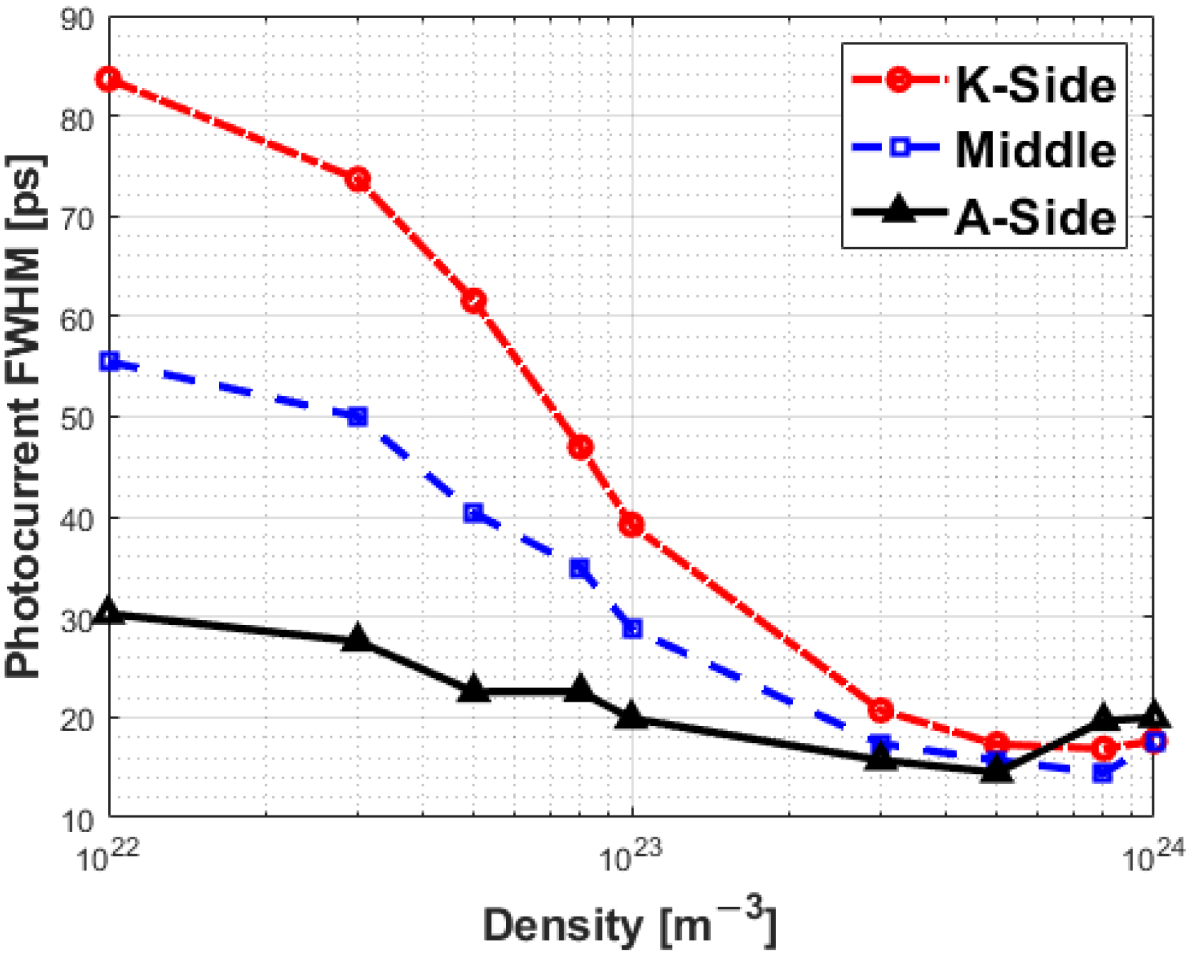
The above results highlight a pattern that increased carrier density would make the location of the photoexcitation region less of an important factor in determining the FWHM of the current pulse. A clearer illustration of this is shown in
Figure 5 which provides simulation results for the photocurrent FWHM as a function of the generated carrier densities in the carbon-doped p-i-n PCSS. Values were obtained for three locations of the photogeneration, center of the 12 μm device, a spot 3 μm from the anode, and a region 3 μm from the cathode. The highest FWHM value is predicted to be ~85 ps for the 25 ps laser pulse at the 10
23 m
−3 density, and occurs for illumination near the cathode side. The corresponding values at this density for the central and anode-side illumination were ~56 ps and ~30 ps, respectively. At early times, the FWHM of the output current pulse is shown to be almost three times longer than the FWHM of the closest (anode-side) location. Furthermore, the results of
Figure 5 reveal that increasing the carrier density by a factor of about ten has significant effects in cutting down the FWHM of the current pulse by more than half. This behavior of reduced FWHM with increasing carrier density is qualitatively preserved in our results. An important outcome of
Figure 5 is that for densities at or greater than ~5 × 10
23 m
−3, the FWHM values are seen to be smaller than that of the 25 ps triggering laser pulse. This result is seen to almost hold for all three locations.
One method to probe and clarify the reasons for the changes is to look directly at the population of the valleys over time during the course of the simulation run. Results pertaining to this aspect are shown in
Figure 6a–d for the p-i-n PCSS structure at an average applied field of 200 kV/cm. The results shown correspond to four different excitation densities of 10
22 m
−3, 5 × 10
22 m
−3, 10
23 m
−3, and 5 × 10
23 m
−3. In all cases, there is a quick change of occupancy from the lowest
Г1 valley to the higher
L-M valleys. This is due to energy gain from the applied electric field, followed by inter-valley transfer. This transition from the valley with the lowest effective mass is indicative of the transition into the NDM regime. Though there are some fluctuations between the
Г1 and the
L-M valleys at the early times, relatively stable conditions are predicted to be reached after about 70 ps, at least for the 10
22 m
−3 and 5 × 10
22 m
−3 cases. At higher densities, (e.g., 10
23 and 5 × 10
23 m
−3), one can see that at times starting around 35 ps, the occupancy in the primary valley begins to increase. This time is directly in line with the peak of the photoexcitation pulse shown in
Figure 1. Since initial creation of electrons is always in the lowest
Г1 valley, it is not surprising that this population (denoted as valley 1 in
Figure 6) rise coincides with the maxima of the illumination pulse. Furthermore, for the high density cases (10
23 m
−3 and 5 × 10
23 m
−3), the internal polarization effect begins to take effect, and leads to a collapse in the local fields at regions between the carbon-doped region and the anode. The field lowering, in turn drives some of the electrons back into the lowest
Г1 valley. The resulting outcome is the transient minima in valley 1 population, best seen in
Figure 6d. The polarization driven internal field collapse is crucial to the overall effect on pulse compression. Since the PCSS is driven in the NDM regime, any lowering of the electric field enhances the drift velocity. This as already shown in the schematic of
Figure 1 applies to electrons at the trailing edge of the photogenerated cloud. Those at the leading edge, are locations further downstream and closer to the anode. The fields in this section are higher, and consequently the drift velocities are lower, and results in the slowing of the leading edge. The net effect is a pulse compression as the trailing edge catches up somewhat with the leading edge.
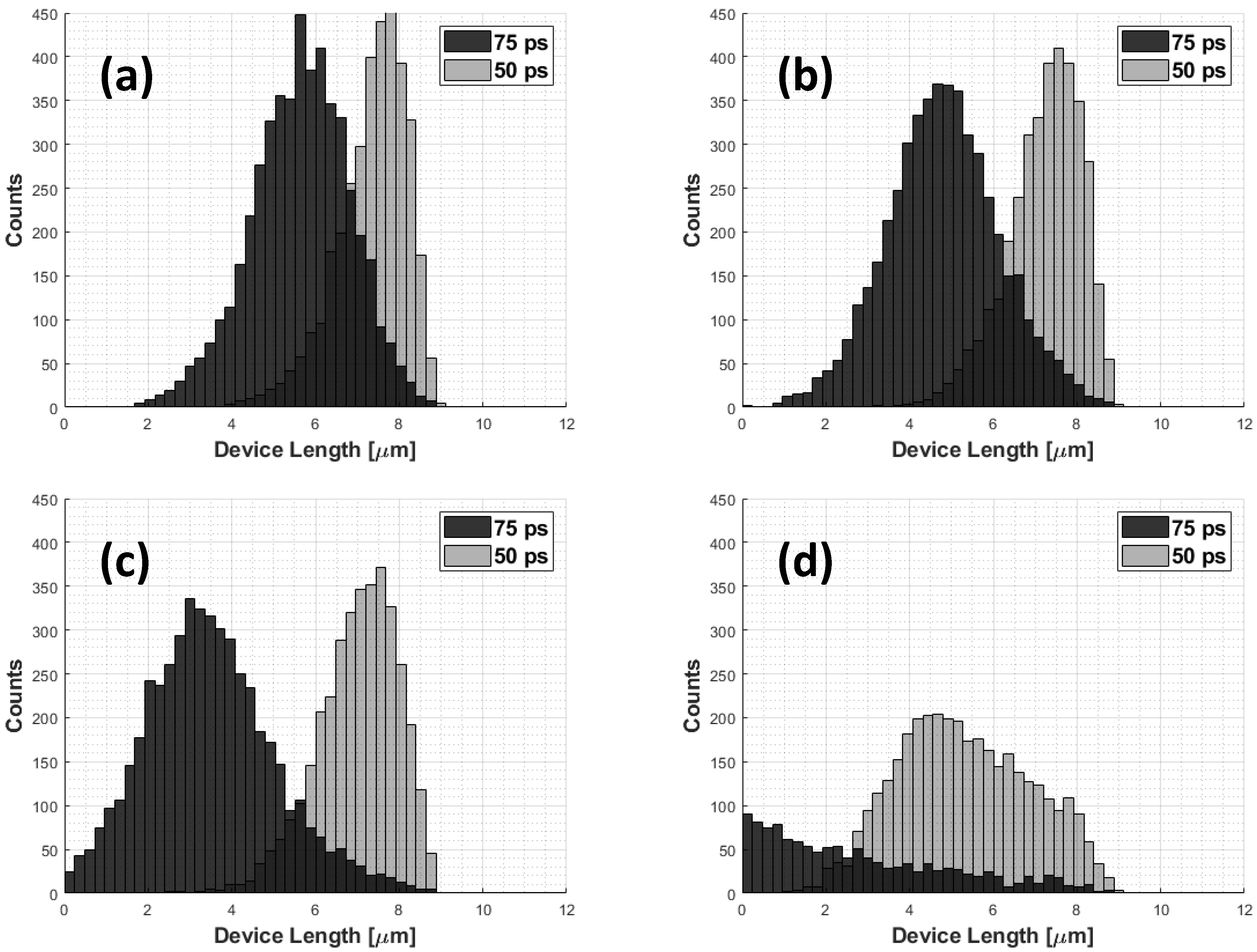
Finally, the spatial profiles of the electron clouds are shown in
Figure 7a–d. The simulation results show snapshots of the time-dependent population of photogenerated electrons at 50 ps and 75 ps time instants again for the four excitation densities of 10
22 m
−3, 5 × 10
22 m
−3, 10
23 m
−3, and 5 × 10
23 m
−3. The electrons were taken to be photogenerated within the 1 μm carbon-doped GaN layer at layer at a distance of 3 μm from the cathode side of the 12 μm long reversed biased p-i-n PCSS. A 25 ps laser pulse was assumed with 5000 simulated electrons. The simulation included implementation of Pauli exclusion, non-parabolic bands, and an electrostatic solver based on the fast multipole method.
Figure 7a–d how the leftward motion of the electron swarm to progressively increase with the photogenerated density. In
Figure 7a at the lowest 10
22 m
−3 density, the leading edge of the swarm at the 75 ps instant is seen to be at around 2 μm. In comparison, the leading edge of the swarm at a higher density of 5 × 10
22 m
−3 is seen to have reached ~1 μm during the 75 ps span. At even higher densities of 10
23 m
−3 and 5 × 10
23 m
−3, the swarms in
Figure 7c,d, respectively, can be seen to have reached the anode on the far left. Furthermore, due to the electron outflow, a lower population remains at the 75 ps instant for the 5 × 10
23 m
−3 density in
Figure 7d. As a result, the peak has the lowest value at about 200 electrons. In general, the peak values in
Figure 7a–c progressively decrease, as the swarms spreads out by increasing amounts. This faster collective motion of the group can be associated with two factors: (i) Due to pulse compression, the trailing edge moves faster and closer to the leading edge on the left. This process leads to a speed up. (ii) The occupancy of the lowest
Г1 valley (having the lowest effective mass) increases at higher density as already seen and discussed in connection with
Figure 6d. The marginal increases in
Г1 valley occupancy in going from 1 × 10
22 m
−3 to 5 × 10
22 m
−3 also helps increase the average drift velocity of the swarm.
These above results collectively point to a potential method for compression of a photocurrent pulse in a PCSS device. The strategy solely relies on factors and behavior inherent to material system. Three related effects that combine to yield the favorable outcome include: (i) the existence of an NDM regime, (ii) the internal field collapse made possible by the polarization effects, and (iii) density dependence of the polarization effect that can strengthen pulse compression with increases in the incident illumination intensity. The present simulations show that though the use of high density photogeneration in GaN-based PCSS devices, it is possible to reduce and even shrink the output current pulse duration below that of the optical pulse. Specifically, in the cases studied, the output photocurrent duration could be compressed and made smaller than the 25 ps temporal scale of the input laser pulse.
4. Conclusions
Solid-state devices have been becoming important in the amplifier space for years as the need for more compact devices that can operate at higher power densities and under harsh environments is becoming more apparent and acute. GaN continues to be a popular material for such applications requiring robust and rugged operation in this arena as it displays significant electrical and thermal durability, higher power handling capability, larger breakdown strengths, and lower dark currents, while reducing on-resistance and power losses. The suitability of GaN-based components for systems that might generate significant output power at high frequencies (on the order of 100 GHz) is studied in this work. The possibility of reducing the FWHM of output current pulses has been shown through comprehensive simulations. This result implies that GaN operated devices would be used in systems capable of generating high output power at gigahertz frequencies.
Our Monte Carlo simulations are best suited for such analysis since they capture nonequilibrium phenomena and can model transient non-Markovian behavior very well. By comparison, other techniques such as those based on the drifty-diffusion equation or hydrodynamic solution based on continuum theory are known to be ill-suited for analyses at these ultrafast time scales [
43]. Future development of GaN-based quantum well heterostructures could offer even greater benefits in the future and would need to be probed carefully.
Results given in this contribution predict pulse compression at fields at or above 200 kV/cm, provided carrier densities of 3 × 10
23 m
−3 or greater can be photogenerated. This compression has been predicted to be robust and independent of the position of the photoexcited region. The outcome has been explained on the basis of three coupled processes, namely: (i) the existence of an NDM regime, (ii) the strong internal field collapse made possible by the polarization effects, and (iii) density dependence of the polarization effect that could work to strengthen the pulse compression with increasing illumination intensity. While direct density-dependent effects have not been experimentally measured as of yet due to the demands of purity and defect-free fabrication of high quality GaN, this study points to promising high power, high frequency applications based on PCSS switches. While direct density-dependent effects have not been experimentally measured as of yet due to the demands of purity and defect-free fabrication of high quality GaN, similar trends have been detailed recently in GaAs. In GaAs material, which has a bandstructure qualitatively similar to GaN, the output PCSS photocurrent full width at half maxima (FWHM) were seen to reach values just slightly lower than the input laser [
35]. Some of the obstacles preventing the successful device testing in GaN are issues arising from material purity. A related difficulty has been the attainment of high holdoff voltages close to the theoretical predicted limits. Without successfully attaining the high fields required for NDM operation (which are roughly on the order of 200 kV/cm), the pulse compression cannot be achieved. To solve this problem, complex geometries are being explored as a way to alleviate the voltage breakdown issue. For example, a relatively recent report points to the possibility of holdoff voltages of about 260 kV/cm [
52]. However, these devices did not use the C-doped layer that is central to the present high-speed operation. However, progress on the device fabrication side is being made [
53,
54]. Hence, it is likely that a true high-speed pulse compression GaN PCSS may be realized in the near future that is capable of operating in the 100 GHz regime as predicted here for a rugged and robust advanced high power PCSS alternative.


