Article

Optimal Bias Condition of Dummy WL for Sub-Block GIDL Erase Operation in 3D NAND Flash Memory

Department of Electronics Engineering, Korea National University of Transportation, Room No. 326, Smart ICT Building, 50 Daehak-ro, Chungju-si 27469, Korea
*
Author to whom correspondence should be addressed.
Electronics 2022, 11(17), 2738; https://doi.org/10.3390/electronics11172738
Submission received: 31 July 2022 / Revised: 23 August 2022 / Accepted: 29 August 2022 / Published: 31 August 2022
(This article belongs to the Special Issue Development and Application of New CMOS Devices)

Abstract

:
In this study, we have analyzed the optimal bias condition of dummy WL for the sub-block gate induced drain leakage (GIDL) erase operation in 16-layer 3D NAND flash memory. Three-dimensional NAND flash memory performs an erase operation in units of pages. Increasing the number of stacks increases the number of cells that are erased at one time, which can lead to undesirable durability degradation. In this case, the sub-block erase operation can reduce the burden on the cell by up to half, due to the erase operation. The distribution of the hole density (hDensity) and the potential, according to VDummy, was analyzed when block1 and block2 were erased by setting WL0:WL7 to block1, WL9:WL15 to block2, and WL8 to dummy WL. For the simulation results, block1 showed an optimal distribution of hDensity and potential in the order of 20 V, floating, and 0 V. In block2, the optimal distribution of hDensity was shown in the order of 20 V, floating, and 0 V, with the optimal distribution of the potential in the order of floating and 0 V.

1. Introduction

Three-dimensional NAND flash memory is currently the most popular memory device and is being actively applied in various fields, such as SSD and flash memory [1]. As of 2013, 3D NAND flash memory has achieved growth, in both capacity and performance, by overcoming limits through vertical stacking in planar NAND, which uses existing floating gates [2,3,4,5,6]. However, this development trend has increased the block size of the 3D NAND [7,8,9,10]. In the bit-cost scalable (BiCS) architecture, the channel is connected to the common source line (CSL), so the body bias cannot be applied directly to the channel. For this reason, we use the GIDL deletion method in CSL to inject holes into the channel in order to increase the channel potential. Due to the structural characteristics of using common source line, the program/erase cycle increases in proportion to the increasing block size in the 3D NAND that performs the erase operation in units of blocks. When the program/erase cycle is increased, the reliability of the device decreases due to various problems, such as the deterioration of the retention characteristics caused by the heat that is generated during the P/E operation, cell disturbance caused by the P/E operation, and the deterioration of the durability of the blocking oxide [11,12,13,14,15,16,17]. This problem can be improved by using a dummy WL to split the blocks and to erase only the selected blocks [18,19,20,21]. In this case, the bias condition of the dummy WL affects the neighboring cells, because the bias that is applied to the dummy WL affects the channel potential according to the coupling ratio of the gate dielectrics [22,23,24,25]. Therefore, the optimal dummy WL bias condition means a state in which the neighboring cells can operate normally without causing a disturbance [26]. During the GIDL erase operation, the channel potential increases to almost the VErase that is applied to the CSL [27]. Based on these characteristics, six cases were simulated, including the condition of selecting block1 and block2 with the bias conditions of VDummy set to VErase, 0V, and floating. For fast and efficient simulation, a random string was selected from the 16-layer 3D NAND flash memory structure, as shown in Figure 1, and the GIDL erase operation was performed in order to analyze the potential difference between the channel and WL.

2. Simulation Design and Results

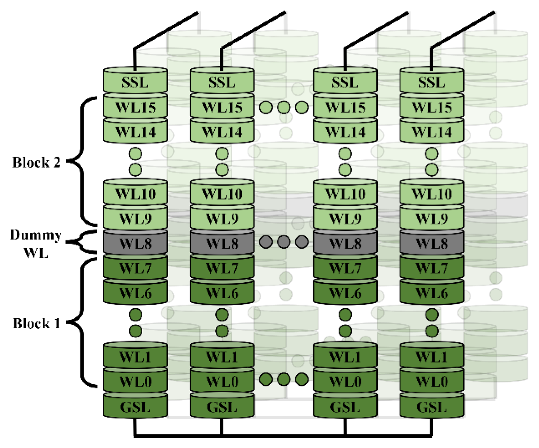
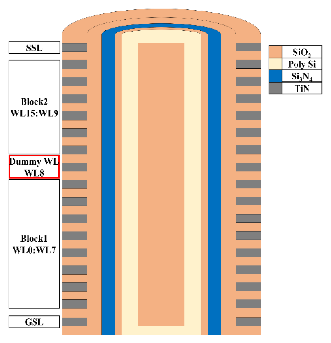
2.1. 3D NAND Flash Memory Structure Setup

Figure 2 shows a cross-section of the 3D NAND flash memory structure that is used in technology computer-aided design (TCAD) simulation. The gate length was set to 30 nm for all of the main cells, string select line (SSL), and ground select line (GSL), and the gate spacing was also set to 30 nm. The thickness of the oxide/nitride/oxide (O/N/O), which is a dielectric constituting the center of the gate, was set to 4/8/8 nm, respectively [24]. Block1 was set as WL0:WL7 and block2 was set as WL9:WL15, which was divided into two blocks based on WL8 set as dummy WL.

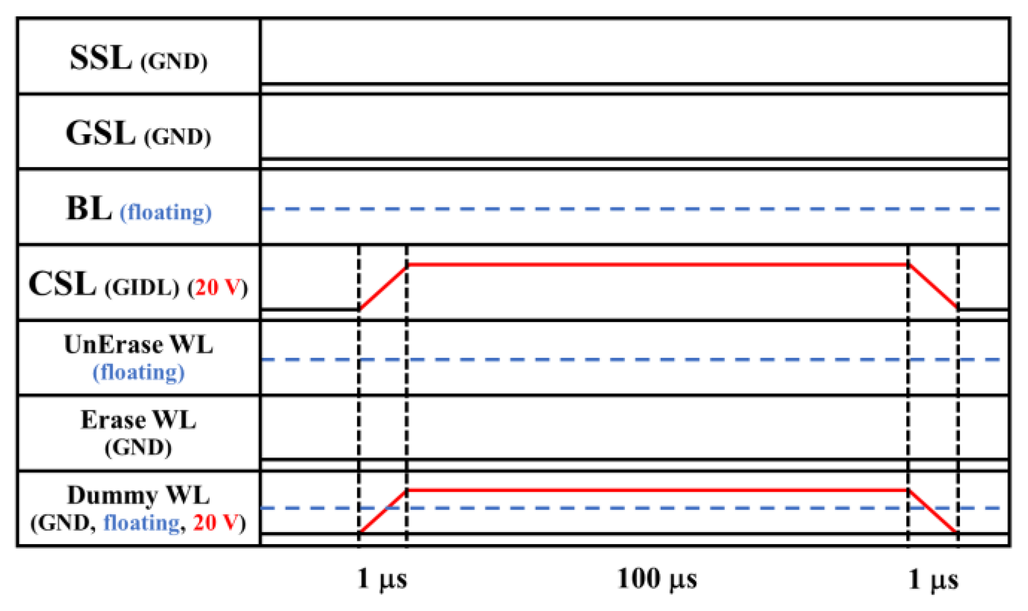
2.2. Simulation Setup

Figure 3 shows the timing diagram that was used for sub-block erase. For the erase operation, 0 V was applied to SSL and GSL, and 20 V VErase was applied to CSL. At this time, GIDL was generated by the potential difference between CSL and GSL; channel electrons leaked out and the channel potential rose. The WL of the Un-erase block was set to floating in order to reduce the potential difference between the channel and WL. A total of 0 V was applied to the WL of the Erase block in order to induce a potential difference between the channel and WL. The voltage of the dummy WL was simulated under the following three conditions: 20 V (VErase), 0 V, and floating.

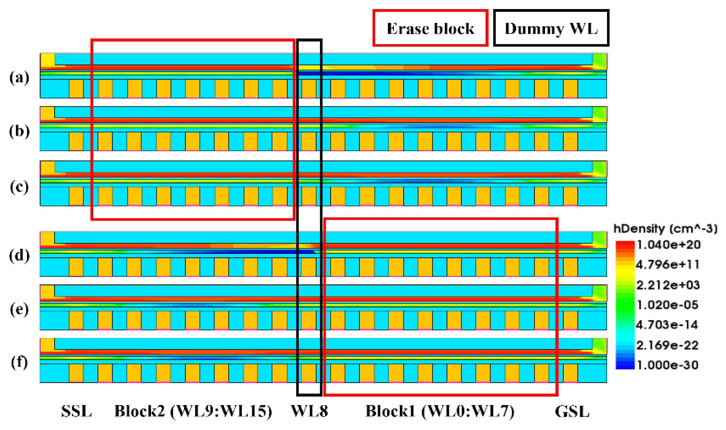
2.3. Analysis of hDensity

Figure 4 shows the hDensity of the cross-section of the selected string after applying VErase to CSL for 100 µs. Figure 4a–c performed the erase operation in block2 (WL9:WL15), and Figure 4d–f performed the erase operation in block1 (WL0:WL7). The bias condition of the dummy WL was set to 20 V, 0 V, and floating. In the case of Figure 4a,d where 20 V was applied to VDummy, it was confirmed that the hDensity of the channel and the nitride was maintained less in the direction of the Un-erase block near to the dummy (WL) than in the other cases.

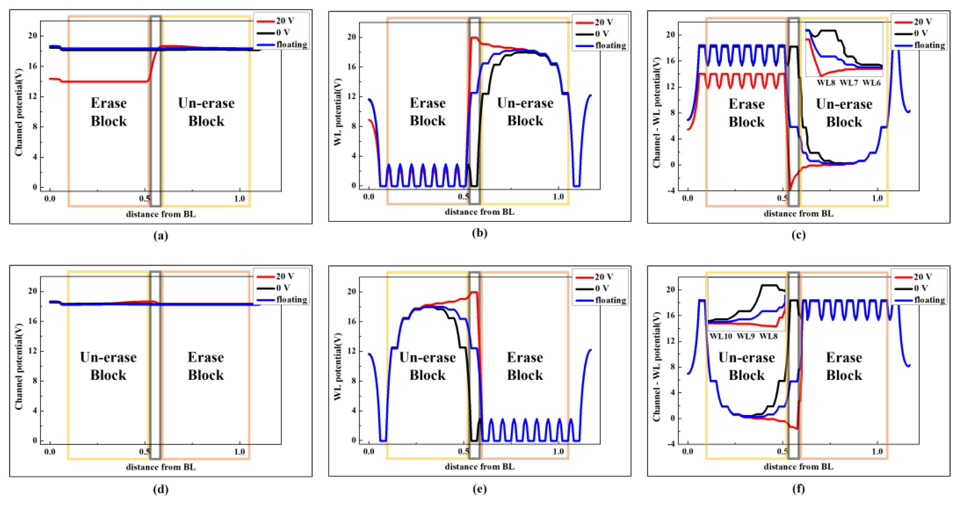
2.4. Analysis of Potential to Channel and WL

Figure 5 shows the channel and WL potential of the selected string after applying VErase to CSL for 100 µs. The bias condition of the dummy WL affected the adjacent WL, WL7, and WL9. The adjacent WLs were more affected when they were included in an Un-erase block than in an Erase block. This is because the WL in the Un-erase block remained floating during the erase phase. In Figure 5a, it was confirmed that the VDummy had the highest channel potential when it was maintained in a floating state. Figure 5b shows the best WL potential in the Un-erase block when the VDummy was 20 V. Figure 5c shows the potential that was obtained by subtracting Figure 5b from Figure 5a, which is the potential difference between the channel and WL. In the Erase block, the potential difference should be large, and in the Un-erase block, the potential difference should be close to zero in order to avoid unwanted erase disturbance. In Figure 5c, when the VDummy was 20 V, the WL7 and WL6 that were adjacent to the dummy WL showed a potential difference that was optimized for the Un-erase block but showed an inadequate potential difference of approximately 14 V in the Erase block. In Figure 5d, when the VDummy was 20 V, the channel potential difference was almost the same. In Figure 5e, almost the same potential was measured in the Erase block, and the most ideal potential was shown in the Un-erase block when the VDummy was 20 V. Figure 5f shows the potential that was obtained by subtracting Figure 5e from Figure 5d. Unlike the result shown in Figure 5c, an appropriate potential difference was measured in the Erase block, even when 20 V was applied to the VDummy. The WL9 and WL10, which were adjacent to the dummy WL, showed a potential difference close to zero, showing the potential suitability of the Un-erase block. In the channel and WL potential simulation results, the optimal VDummy showed a different order when performing the erase operation in block1 and block2. When the erase operation was performed on block1 close to the CSL, the optimal potential was shown in the order of 20 V, floating, and 0 V. When performing the erase operation on block2 far from the CSL, only floating and 0 V could be used as the VDummy, and 20 V was confirmed to be an unsuitable voltage for the VDummy.

3. Conclusions

In the simulation results of the channel and WL potential, the optimal VDummy was confirmed to be in a different order, according to the selected block during the erase operation. It was confirmed that the hDensity in the nitride layer of the Un-erase block could be effectively lowered if VErase and VDummy are applied at the same level when erasing block1 and block2. In particular, a lower hDensity was confirmed at the bottom of WL8, which was set as the dummy WL. This is because the high VDummy that was applied to the dummy WL prevents tunneling. Therefore, it was confirmed that the VDummy showed the ideal hDensity in the order of 20 V, floating, and 0 V. In the channel and WL potential measurement results, the optimal VDummy showed a different order when performing the erase operation. In the case where block1 was set as the Erase block, the optimal potential distribution was shown in the order of 20 V, floating, and 0 V. In the case where block2 was set as the Erase block, a VDummy of 20 V reduced the channel potential of the Erase block to 14 V, thereby reducing the erase efficiency. In this case, it was confirmed that the optimized potential distribution appeared in the order of floating, 0 V, and 20 V.

Author Contributions

Investigation, B.K.; data curation, B.K.; visualization, B.K.; software, B.K.; validation, B.K.; formal analysis, B.K.; writing, B.K.; supervision, M.K.; project administration, M.K.; funding acquisition, M.K. All authors have read and agreed to the published version of the manuscript.

Funding

This research was supported by Basic Science Research Program through the National Research Foundation of Korea (NRF) funded by the Ministry of Education (2018R1A6A1A03023788) and in part by the Institute of Information and Communications Technology Planning and Evaluation (IITP) funded by the Korea government (MSIT) under Grant 2021-0-01764 and in part by the National R&D Program through the National Research Foundation of Korea (NRF) funded by Ministry of Science and ICT (2021M3F3A2A03017693).

Conflicts of Interest

The authors declare no conflict of interest.

References

  1. Choe, J. Memory Technology 2021: Trends & Challenges. In Proceedings of the 2021 International Conference on Simulation of Semiconductor Processes and Devices (SISPAD), Granada, Spain, 27–29 September 2021; pp. 111–115. [Google Scholar] [CrossRef]
  2. Kang, M.; Lete, K.; Chale, D.H.; Park, B.-G.; Shin, H. The compact modeling of channel potential in Sub-30-nm NAND flash cell string. IEEE Electron Device Lett. 2012, 33, 321–323. [Google Scholar] [CrossRef]
  3. Park, Y.; Lee, J.; Cho, S.S.; Jin, G.; Jung, E. Scaling and reliability of NAND flash devices. In Proceedings of the 2014 IEEE International Reliability Physics Symposium, Waikoloa, HI, USA, 1–5 June 2014. [Google Scholar] [CrossRef]
  4. Kim, Y.; Kang, M. Predictive modeling of channel potential in 3-D NAND flash memory. IEEE Trans. Electron Devices 2014, 61, 3901–3904. [Google Scholar] [CrossRef]
  5. Kim, H.; Ahn, S.-J.; Shin, Y.G.; Lee, K.; Jung, E. Evolution of NAND Flash Memory: From 2D to 3D as a Storage Market Leader. In Proceedings of the 2017 IEEE International Memory Workshop (IMW), Monterey, CA, USA, 14–17 May 2017; pp. 1–4. [Google Scholar] [CrossRef]
  6. Li, Y. 3D NAND memory and its application in solid-state drives: Architecture, reliability, flash management techniques, and current trends. IEEE Solid-State Circuits Mag. 2020, 12, 56–65. [Google Scholar] [CrossRef]
  7. Goda, A. 3-D NAND Technology Achievements and Future Scaling Perspectives. IEEE Trans. Electron Devices 2020, 67, 1373–1381. [Google Scholar] [CrossRef]
  8. Goda, A. Recent Progress on 3D NAND Flash Technologies. Electronics 2021, 10, 31563156. [Google Scholar] [CrossRef]
  9. Park, S.; Lee, J.; Jang, J.; Lim, J.K.; Kim, H.; Shim, J.J.; Yu, M.-T.; Kang, J.-K.; Ahn, S.J.; Song, J. Highly-Reliable Cell Characteristics with 128-Layer Single-Stack 3D-NAND Flash Memory. In Proceedings of the 2021 Symposium on VLSI Technology, Hsinchu, Taiwan, 19–22 April 2021; pp. 1–2. [Google Scholar]
  10. Kim, J.H.; Yim, Y.; Lim, J.; Kim, H.S.; Cho, E.S.; Yeo, C.; Lee, W.; You, B.; Lee, B.; Kang, M.; et al. Highly Manufacturable 7th Generation 3D NAND Flash Memory with COP structure and Double Stack Process. In Proceedings of the 2021 Symposium on VLSI Technology, Hsinchu, Taiwan, 19–22 April 2021; pp. 1–2. [Google Scholar]
  11. Fayrushin, A.; Seol, K.; Na, J.; Hur, S.; Choi, J.; Kim, K. The new program/erase cycling degradation mechanism of NAND flash memory devices. In Proceedings of the 2009 IEEE International Electron Devices Meeting (IEDM), Baltimore, MD, USA, 7–9 December 2009; pp. 1–4. [Google Scholar] [CrossRef]
  12. Woo, C.; Kim, S.; Park, J.; Shin, H.; Kim, H.; Choi, G.-B.; Seo, M.-S.; Noh, K.H. Modeling of charge failure mechanisms during the short term retention depending on program/erase cycle counts in 3-D NAND flash memories. In Proceedings of the 2020 IEEE International Reliability Physics Symposium (IRPS), Dallas, TX, USA, 28 April–30 May 2020; pp. 1–6. [Google Scholar] [CrossRef]
  13. Kim, S.; Lee, K.; Woo, C.; Hwang, Y.; Shin, H. Analysis of Failure Mechanisms During the Long-Term Retention Operation in 3-D NAND Flash Memories. IEEE Trans. Electron Devices 2020, 67, 5472–5478. [Google Scholar] [CrossRef]
  14. Chiu, Y.-Y.; Chang, K.-C.; Lin, H.-J.; Tsai, H.-T.; Lin, P.-J.; Li, H.-C.; Takeshita, T.; Yano, M.; Shirota, R. Impact of Program/Erase Cycling Interval on the Transconductance Distribution of NAND Flash Memory Devices. IEEE Trans. Electron Devices 2020, 67, 4897–4903. [Google Scholar] [CrossRef]
  15. Wang, Y.; Tan, J.; Mao, R.; Li, T. Temperature-Aware Persistent Data Management for LSM-Tree on 3-D NAND Flash Memory. IEEE Trans. Comput. Aided Des. Integr. Circuits Syst. 2020, 39, 4611–4622. [Google Scholar] [CrossRef]
  16. Luo, Y.; Ghose, S.; Cai, Y.; Haratsch, E.F.; Mutlu, O. Improving 3D NAND Flash Memory Lifetime by Tolerating Early Retention Loss and Process Variation. Proc. ACM Meas. Anal. Comput. Syst. 2018, 2, 1–48. [Google Scholar] [CrossRef]
  17. Wang, Y.; Huang, J.; Chen, J.; Mao, R. PVSensing: A Process-Variation-Aware Space Allocation Strategy for 3D NAND Flash Memory. IEEE Trans. Comput. Aided Des. Integr. Circuits Syst. 2022, 41, 1302–1315. [Google Scholar] [CrossRef]
  18. Jeong, Y.; Ham, I.; Han, S.; Kang, M. Optimal dummy word line condition to suppress hot carrier injection phenomenon due to the natural local self-boosting effect in 3D NAND flash memory. Jpn. J. Appl. Phys. 2020, 59, 1–5. [Google Scholar] [CrossRef]
  19. Han, S.; Jeong, Y.; Jhon, H.; Kang, M. Investigation of inhibited channel potential of 3D NAND flash memory according to word-line location. Electronics 2020, 9, 268. [Google Scholar] [CrossRef]
  20. Lee, S.; Kim, C.; Kim, M.; Joe, S.-M.; Jang, J.; Kim, S.; Lee, K.; Kim, J.; Park, J.; Lee, H.-J.; et al. A 1Tb 4b/cell 64-stacked-WL 3D NAND flash memory with 12MB/s program throughput. In Proceedings of the 2018 IEEE International Solid-State Circuits Conference, ISSCC 2018, San Francisco, CA, USA, 11–15 February 2018; pp. 340–342. [Google Scholar] [CrossRef]
  21. Jo, H.; Shin, H. New Read Schemes to Reduce Read Disturbance Due to HCI in Full Boosting Channel 3-D NAND Flash Memories. In Proceedings of the 2021 Silicon Nanoelectronics Workshop (SNW), Virtual Conference. 13 June 2021; pp. 1–2. [Google Scholar]
  22. Kim, Y.; Kang, M. Down-coupling phenomenon of floating channel in 3D NAND flash memory. IEEE Electron Dev. Lett. 2016, 37, 1566–1569. [Google Scholar] [CrossRef]
  23. Kang, M.; Kim, Y. Natural local self-boosting effect in 3D NAND flash memory. IEEE Electron Dev. Lett. 2017, 38, 1236–1239. [Google Scholar] [CrossRef]
  24. Breuil, L.; Nyns, L.; Banerjee, K.; Palayam, S.V.; Subirats, A.; Richard, O.; Conard, T.; Bosch, G.V.D.; Furnemont, A. Impact of SiON tunnel layer composition on 3D NAND cell performance. In Proceedings of the 2019 IEEE 11th International Memory Workshop (IMW), Monterey, CA, USA, 12–15 May 2019; pp. 1–4. [Google Scholar] [CrossRef]
  25. Monzio Compagnoni, C.; Spinelli, A.S. Reliability of NAND Flash Arrays: A Review of What the 2-D–to–3-D Transition Meant. IEEE Trans. Electron Devices 2019, 66, 4504–4516. [Google Scholar] [CrossRef]
  26. Jeong, Y.; Ham, I.; Kang, M. Optimal bias condition of dummy WL for sub-block erase operation in 3D NAND flash memory. In Proceedings of the 2019 International Conference on Solid State Devices and Materials, Aichi, Japan, 2–5 September 2019; pp. 683–684. [Google Scholar]
  27. Malavena, G.; Lacaita, A.L.; Spinelli, A.S.; Monzio Compagnoni, C. Investigation and compact modeling of the time dynamics of the GIDL-assisted increase of the string potential in 3-D NAND flash arrays. IEEE Trans. Electron Devices 2018, 65, 2804–2811. [Google Scholar] [CrossRef]
Figure 1. Cell array of 3D NAND flash memory.
Electronics 11 02738 g001
Figure 2. Schematic cross-section of 3D NAND flash memory structure used in TCAD simulation.
Electronics 11 02738 g002
Figure 3. Timing diagram used in TCAD simulation.
Electronics 11 02738 g003
Figure 4. hDensity due to VDummy after VErase input 100 µs, block2 and VDummy (a) 20 V, (b) 0 V, (c) floating, block1 and VDummy (d) 20 V, (e) 0 V, (f) floating.
Electronics 11 02738 g004
Figure 5. (a) Channel, (b) WL, (c) Channel–WL potential by VDummy during erase operation in block2, (d) Channel, (e) WL, (f) Channel–WL potential by VDummy during erase operation in block1.
Electronics 11 02738 g005
Publisher’s Note: MDPI stays neutral with regard to jurisdictional claims in published maps and institutional affiliations.

