Article

A 26–30 GHz GaN HEMT Low-Noise Amplifier Employing a Series Inductor-Based Stability Enhancement Technique

1
Department of Radio and Information Communication Engineering, Chungnam National University, Daejeon 34134, Korea
2
ICT Creative Research Lab, Electronics and Telecommunication Research Institute (ETRI), Daejeon 34129, Korea
3
Wavepia Incorporated, Hwaseong-si 18469, Korea
*
Author to whom correspondence should be addressed.
Electronics 2022, 11(17), 2716; https://doi.org/10.3390/electronics11172716
Submission received: 4 July 2022 / Revised: 16 August 2022 / Accepted: 26 August 2022 / Published: 30 August 2022
(This article belongs to the Special Issue RF/Microwave Circuits for 5G and Beyond)

Abstract

:
This article presents a 26–30 GHz gallium nitride (GaN) high electron mobility transistor (HEMT) low-noise amplifier (LNA) for fifth-generation base station applications. In the proposed design, a series inductor-based stability enhancement technique was utilized to improve the reverse isolation and stability performance of the amplifier and to mitigate the effect of the parasitic capacitance of the GaN HEMT device. To validate the concept of the design, a three-stage GaN HEMT LNA was designed and fabricated in a 0.15-um GaN on silicon carbide technology. The demonstrated design achieved a gain of 20.2 dB, a noise figure of 2.4–2.5 dB, an output 1-dB compression point of 17.2 dBm, and an output third-order intercept point of 32.2 dBm. The design also attained stability (μ criterion) up to 7.7 at the operating frequency. The implemented design consumed power of 320 mW with a nominal supply of 10 V.

1. Introduction

Recently, the commercialization of millimeter-wave (mmWave) fifth-generation (5G) new radio (NR) communication has been actively attempted in various countries to cope with the explosive increase in mobile data traffic. Therefore, extensive research has been conducted to develop and secure high-performance, low-cost, and highly reliable solutions in preparation for full-scale deployment of 5G base stations [1,2]. In reality, the envisioned mmWave 5G NRs adopt massive multiple-input multiple-output (MIMO) technology that utilizes a phased-array antenna configuration. Therefore, small-size, low-cost, and high-linearity radio frequency (RF) front-end modules (FEMs) that integrate low-noise amplifiers (LNAs), high-power amplifiers (PAs), and transmitter/receiver switches are in high demand, specifically for base station applications [3,4]. To satisfy these requirements, a gallium nitride (GaN) high electron mobility transistor (HEMT) has been considered as an attractive candidate for the FEM design of mmWave 5G NR base station applications. In practice, the GaN HEMT device has its own distinct merit with regard to its high power handling capability. This is primarily attributed to the wide energy bandgap (3.4 eV), high saturation velocity (>2.5 × 10⁵ m/s), and high breakdown voltage (>100 V) of GaN HEMT devices [5,6,7]. For this reason, GaN HEMT devices have been widely used in various PA implementations to endure modulated high-power RF signals [8,9,10,11].
Based on the supremacy of GaN devices, the research and development of the GaN HEMT-based LNAs has also been intensified from the perspective of design simplicity, low cost, and enhanced noise performance. In fact, FEMs using gallium arsenide (GaAs) technology have been widely utilized in various wireless applications over the last decade because GaAs devices generally provide good electron mobility and noise characteristics [12,13,14,15]. However, as depicted in Figure 1a, the limited high-power robustness of GaAs devices necessitates additional protection circuits such as an isolator and/or a limiter at the input of the receiver front end, which substantially exacerbates the design complexity and noise performance of the FEM design. On the other hand, a GaN HEMT-based LNA with a single-pole double-throw (SPDT) switch (Figure 1b) no longer needs those protection circuits owing to their own inherent high-power endurance [16]. Therefore, through the elimination of these extra protection circuits, reduced size and improved noise performance can be realized in the FEM design with the additional possibility of a low-cost single-chip solution by integrating the LNA, PA, and SPDT within a single die. Moreover, as the scaling of GaN technology shrinks and corresponding breakdown voltage increases, the noise characteristic of GaN devices becomes comparable to that of their GaAs and indium phosphide (InP) counterparts. Because of these benefits, various GaN HEMT-based LNAs have been reported in recent studies [17,18,19,20,21,22,23,24]. However, in the design of GaN HEMT-based amplifiers, stability performance is also a major concern, which is directly related to the reverse isolation characteristic (S12) of the amplifier. Specifically, in the mmWave frequency range, high frequency path losses and parasitic capacitance readily affect isolation characteristics. This eventually causes an extra design trade-off between stability and maximum available gain (MAG) performance.
In this study, we demonstrate a 26–30 GHz GaN HEMT LNA monolithic microwave integrated circuit (MMIC) using a 0.15-μm GaN-on-silicon carbide (SiC) process. By adopting series inductors at the drains of the device, the reverse isolation and stability performance of the amplifier are eventually improved at the operating frequency with minimum impact on the overall MAG and noise figure (NF) performance. The implemented design is targeted for application in the phased-array antenna structure for 5G base stations, which support the n257 (26.5–29.5 GHz) and n261 (27.5–28.35 GHz) bands of the 5G NR frequency range 2 (FR2) [1]. The remainder of this paper is organized as follows: In Section 2, several performance parameters of the utilized 0.15-μm GaN-on-SiC process are emphasized and compared with those of other mmWave semiconductor devices. Section 3 describes the detailed LNA design with the discussion of the series inductor-based stability enhancement technique. Experimental results are presented in Section 4. Finally, Section 5 concludes the paper.

2. GaN-on-SiC Technology

GaN-on-SiC technology intrinsically offers excellent endurance properties against high temperatures as well as large power signals. In practice, the major characteristics of semiconductor active devices, specifically in the mmWave frequency range, are chiefly estimated by their parameters of electron mobility, energy bandgap, and thermal conductivity. Table 1 lists the major properties of several microwave semiconductor materials, including GaN and SiC. Among the parameters, the electron mobility property is an important criterion for evaluating the high-frequency performance of semiconductor devices; it is closely related to the achievable gain and noise performance of the device. According to Table 1, the electron mobility of GaAs is approximately five times higher than that of GaN. However, owing to advancements in technology, the electron mobility of the GaN has been enhanced accordingly and is currently superior to that of Si. The energy bandgap, which refers to the difference between the valence and conduction bands, determines the breakdown voltage of the device where the electrons attain sufficient energy to move to the conduction band and contribute to the drain current. Therefore, a high energy bandgap is highly associated with a high breakdown voltage, which increases the device endurance against a large power signal. GaN and SiC inherently possess superior energy bandgaps and breakdown voltages compared with GaAs, InP, and Si. Thermal conductivity indicates the material’s capability to dissipate the heat of the device, which is generated by the device’s power consumption. Compared to GaAs, GaN and SiC possess lower thermal resistance and higher thermal conductivity; therefore, GaN and SiC materials are more suitable for high-power PA circuits that need to withstand high temperature conditions.
The GaN HEMT LNA designed in this work was fabricated using the process design kit of NP15-00, a GaN-on-SiC substrate technology with a gate length of 0.15-μm, which was provided by the Win Semiconductors Corporation foundry. Considering the stability, minimum NF, and MAG features at the operating frequency, a transistor size of 4 × 25 μm (4F25) GaN HEMT was chosen, which has a breakdown voltage of more than 120 V, a current gain cutoff frequency (fT) of approximately 34.5 GHz, and a maximum oscillation frequency (fMAX) of approximately 125 GHz. In addition, this process provides two interconnected metal layers, high-reliability metal–insulator–metal capacitors, and precision tantalum nitride resistors for full MMIC designs.

3. Proposed GaN HEMT MMIC LNA Design

In the design of the proposed LNA, small-signal models of the GaN HEMT device, which contain measured S-parameters and NF data with given drain voltage and DC current conditions for the frequency range of 20–40 GHz, were used in the simulation. All required electromagnetic simulations were conducted using an advanced design system momentum tool to precisely model the utilized transmission line-based matching net-works and reflect the parasitic components from capacitors, inductors, and bond pads.

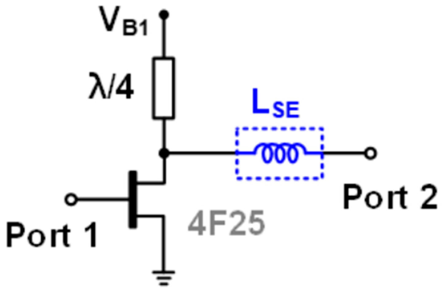
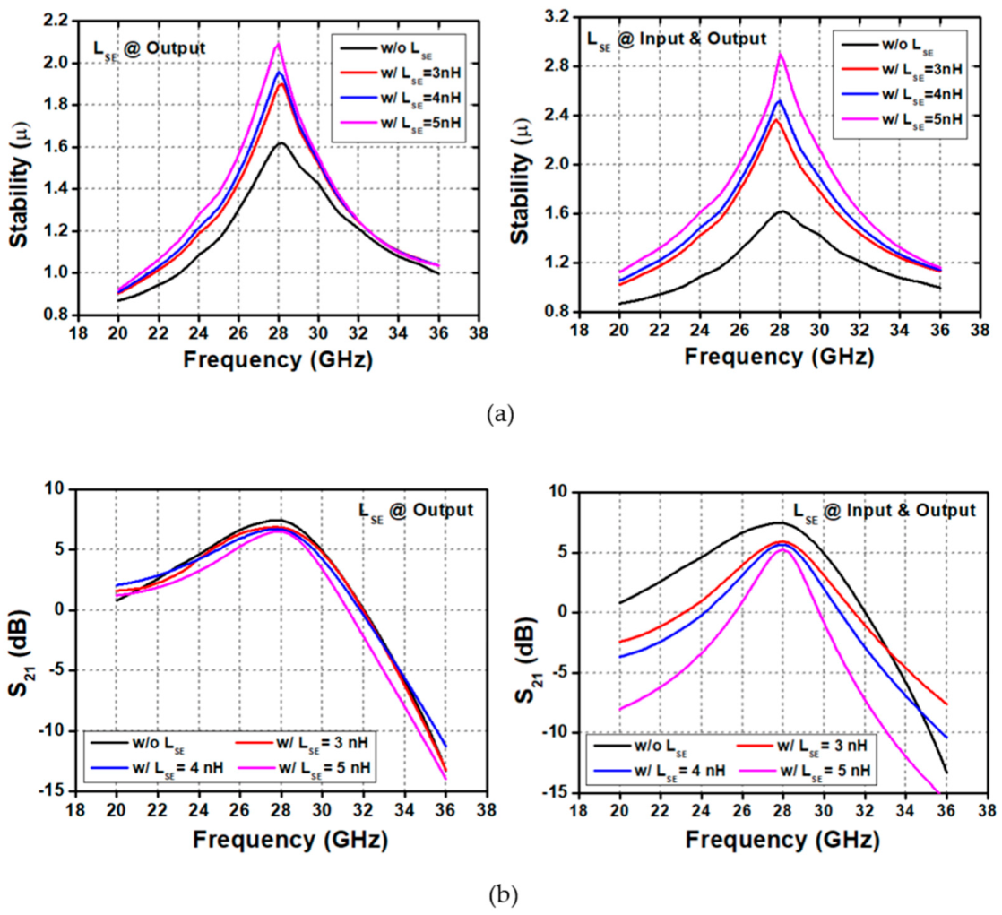
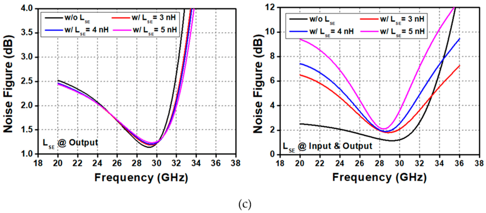
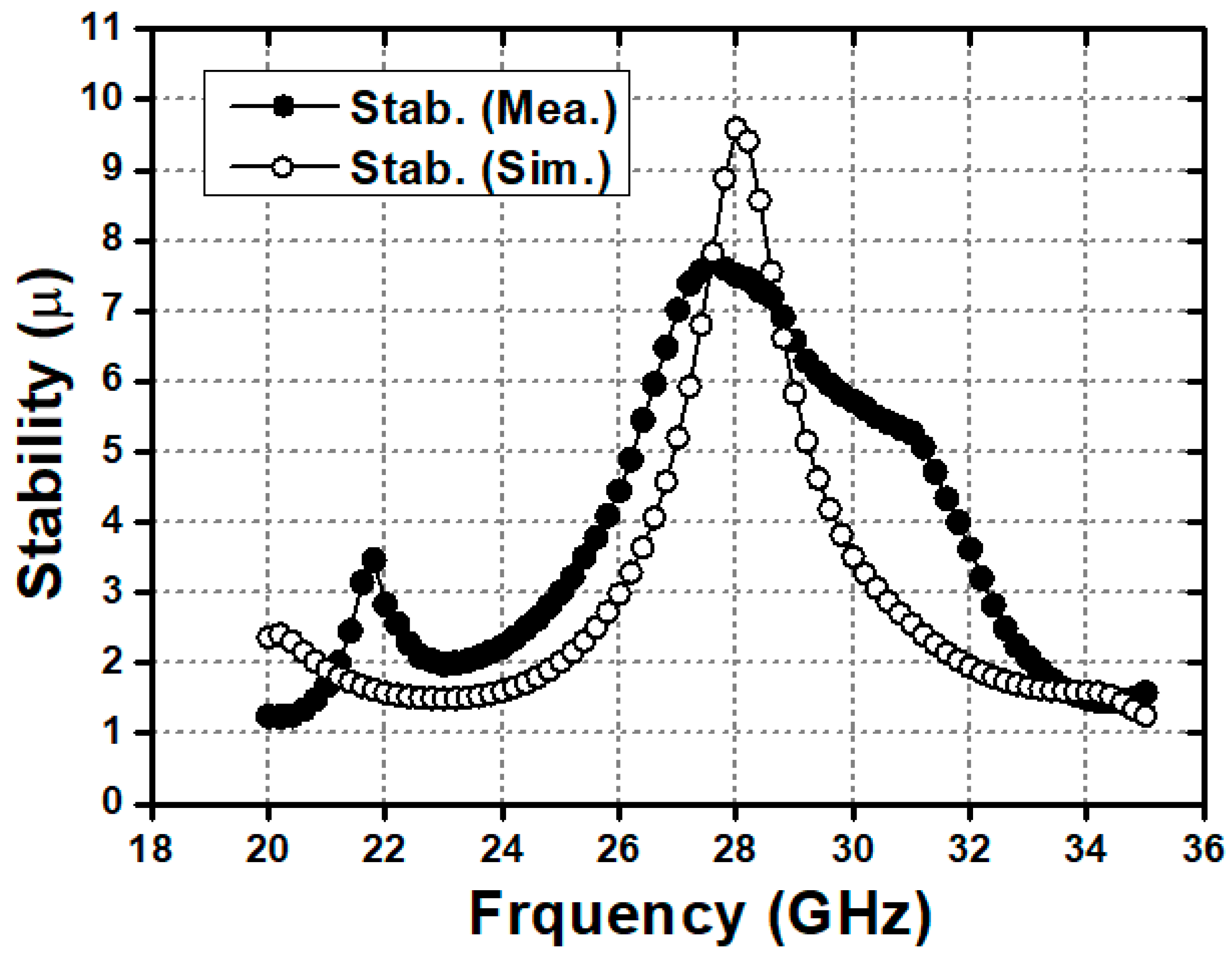
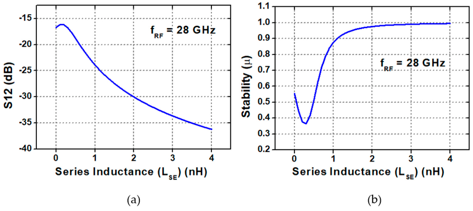
3.1. Reverse Isolation and Stability Performance of GaN HEMT Devices

In reality, the reverse isolation and stability performance of GaN HEMT devices is a serious concern in the mmWave frequency band, which generally requires a design trade-off with the MAG and NF performance for the operation of the amplifier. The reverse isolation and stability characteristics can be mainly evaluated from the scattering parameter (S12) and μ criterion for the designed two-port network, respectively. The S12 primarily indicates the amount of feedback from the output to the input ports. For a single-stage common-source (CS) configuration, a gate-drain capacitance of GaN devices mostly determines the overall reverse isolation performance of the network. The μ criterion is a parameter of stability and is widely used in two-port networks [6,25,26]. The μ criterion, which is defined by the scattering parameters, is expressed as:
μ = 1 S 11 2 S 22 Δ S 11 + S 12 S 21
where Δ denotes the determinant of the scattering matrix, defined as Δ = S11 × S22 − S12 × S21. If the μ value is greater than unity at the operating frequency, it ensures that the network is unconditionally stable. As can be deduced from Equation (1), the μ value is highly related to the reverse isolation of the network; therefore, a smaller S12 is always desirable to securely realize stable operation of the amplifier.
Figure 2 shows the stability enhancement configurations that have been generally applied to MMIC designs. First, a cascode configuration, as shown in Figure 2a, is composed of stacked CS and common-gate (CG) stages and basically offers high reverse isolation from the output to input ports owing to its own shielding effect. Interestingly, as the number of stacked stages increases, the amount of reverse isolation and the corresponding stability are improved accordingly [20]. However, relatively complex independent biasing for each CS and CG device is required to adjust the optimal bias conditions using several supply voltage sources. The source degeneration of the single-stage amplifier in Figure 2b also improves the overall stability by applying a negative feedback through the LS while sacrificing the MAG and noise performance. This approach is also beneficial for achieving linearity enhancement and the possibility of simultaneous power and noise matching in the design. In Figure 2c, the utilized series resistor at the input or output port of the single stage directly increases reverse isolation by providing a higher series impedance. However, this configuration substantially exacerbates the overall gain and noise performance of the amplifier because noisy impedance is added in the signal path.
In the proposed design, a series inductor (LSE) instead of the series resistor is adopted at the output to enhance the stability of the amplifier (Figure 3). Similar to the series resistor-based technique (Figure 2c), it readily decreases S12 and improves reverse isolation by offering a higher output impedance at the operating frequency. However, the proposed technique does not cause significant noise performance degradation owing to its inherently low resistance. Moreover, the added series inductor partially cancels the parasitic capacitance at the output node. Consequently, this mitigates the MAG degradation caused by the series impedance in the signal path. Figure 4 shows the S12 and μ simulation results of the single-stage CS amplifier (4F25) (Figure 3) by adopting different values of the series inductor (LSE) at the drain of the GaN device at 28 GHz frequency. As expected, the simulated S12 and μ values are improved when larger inductors are employed.
In addition, the stability performance of the single-stage CS amplifier was evaluated in simulations with matching networks (MNs) to reflect all the scattering parameters (S11, S12, S21, S22) of the network. Figure 5 depicts the single-stage CS amplifier configurations with matching networks and series inductor(s) at the input and/or output nodes. In these simulations, source degeneration (L = 130 μm and W=15 μm) is also utilized in combination with the series inductor-based technique to further enhance the overall stability performance. The simulated small-signal gains (S21s) and μ values are shown in Figure 6. As can be seen from Figure 6, larger values of LSE result in a more enhanced stability (μ) performance in the overall frequency band. Moreover, when series inductors are utilized at both the input and output ports (Figure 6b), stability performance is further enhanced. Although the small-signal gains (S21s) and NFs of the single-stage amplifiers are degraded owing to the effect of series impedance (LSE) in the signal path, the amount of degradation is mitigated through partial cancellation of the parasitic capacitance at the source or drain node with series inductors.

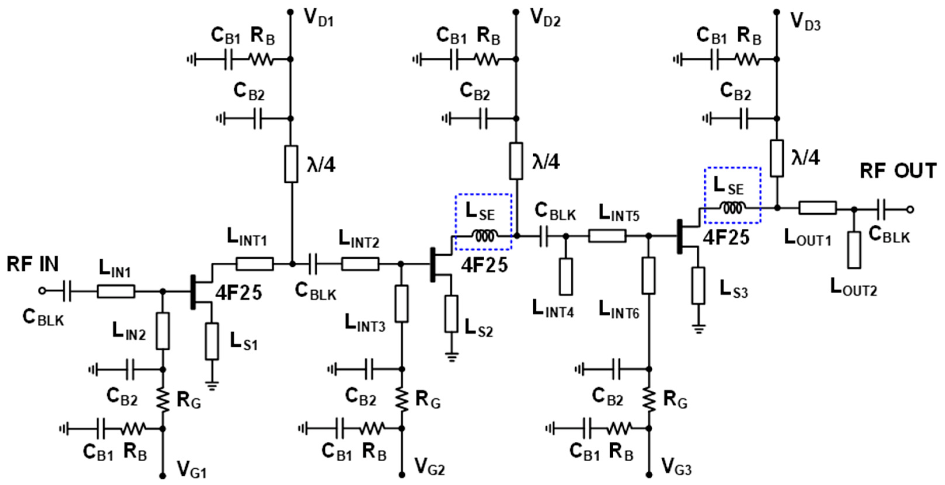
3.2. Three-Stage GaN HEMT-Based LNA Employing a Series Inductor

Figure 7 and Table 2 show a schematic of the designed GaN HEMT LNA MMIC, which includes the bias and matching networks applied to each stage, and values of the utilized components and transmission lines of the designed LNA, respectively. The width of each microstrip line (WTL) is identical at 15 μm. In the proposed design, three cascade CS amplifier stages are configured to attain targeted small-signal gains greater than 20 dB at the desired frequency. To bias utilized GaN HEMT devices, a drain voltage of 10 V is identically applied to each stage through a quarter-wavelength (λ/4) short stub that forms high impedance RF chokes at the operating frequency. On the other hand, the gate terminal of each device is simply biased with –1.7 V through a short stub as a part of the input matching network of the device so that smaller matching and bias configuration can be realized without extra λ/4 biasing short stubs. However, in reality, a DC current flowing through the gate of GaN HEMT devices critically influences the survivability of the LNA and mainly causes device damage by turning on the gate diode or impact ionization during breakdown. In this design, a series gate resistor (RG) of 200 Ω is chosen and applied as voltage feedback to reduce the excessive gate current by shifting the gate voltage to a lower value [16]. Parallel-connected decoupling capacitors of CB1 and CB2 (CB1 = 3.16 pF and CB2 = 0.56 pF) in combination with RB (RB = 10.2 Ω) provides solid ground conditions at the wide frequency range. It also entails the improvement of the stability performance by further suppressing the RF leakage signals through bias networks. Each stage adopts source degeneration to acquire simultaneous power and noise matching as well as stability enhancement, as previously mentioned. Instead of using spiral inductors for source degeneration, microstrip lines (LS1, LS2, and LS3) are used because they are suitable for realizing the required small inductance in the band of interest. In this design, noise matching is primarily considered in the first stage, whereas the second and third stages are designed to optimize the stability and available gain performance. Therefore, the series inductor-based stability enhancement technique is only applied to the drain node of the second and third stages with minimum impact on the MAG and NF performance. Spiral-type series inductors are utilized with careful consideration of the available inductance, self-resonance frequency (SRF), and quality factor (Q-factor). Series inductors of 4.3 nH with the SRF of more than 50 GHz and the Q factor of approximately 22 are utilized in the design.

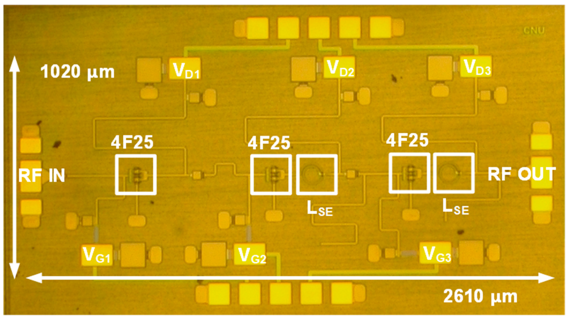
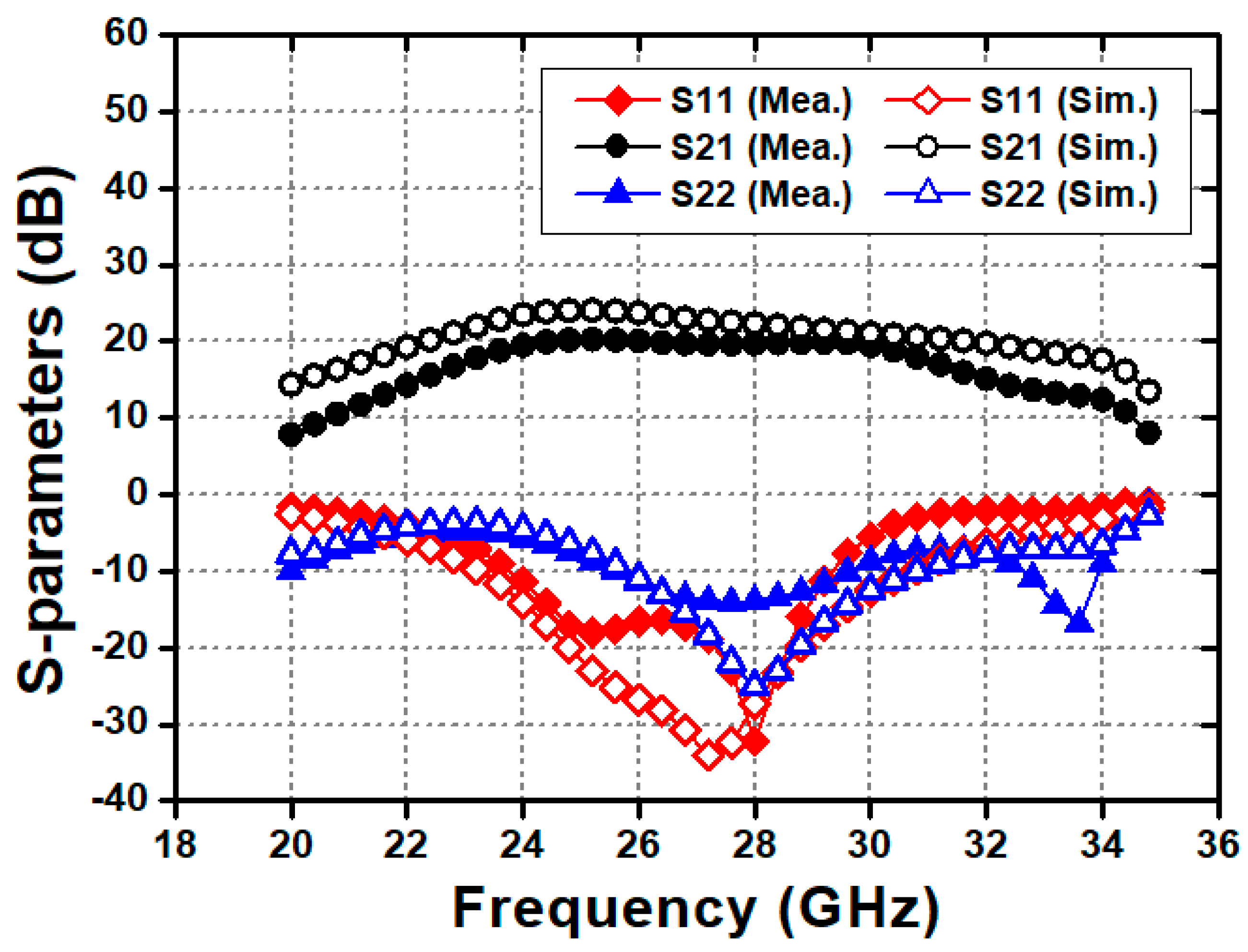
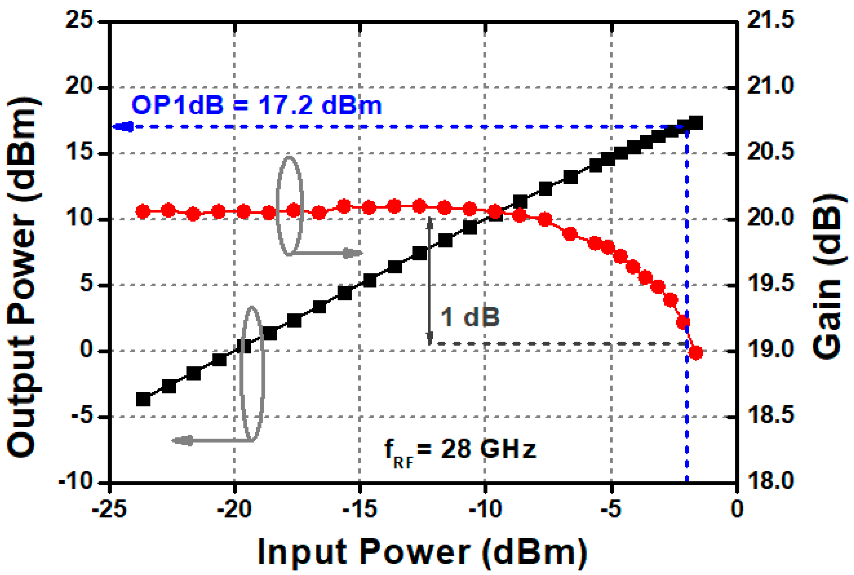
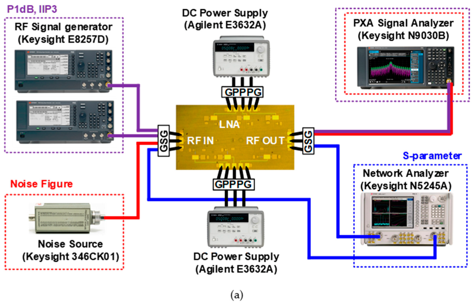
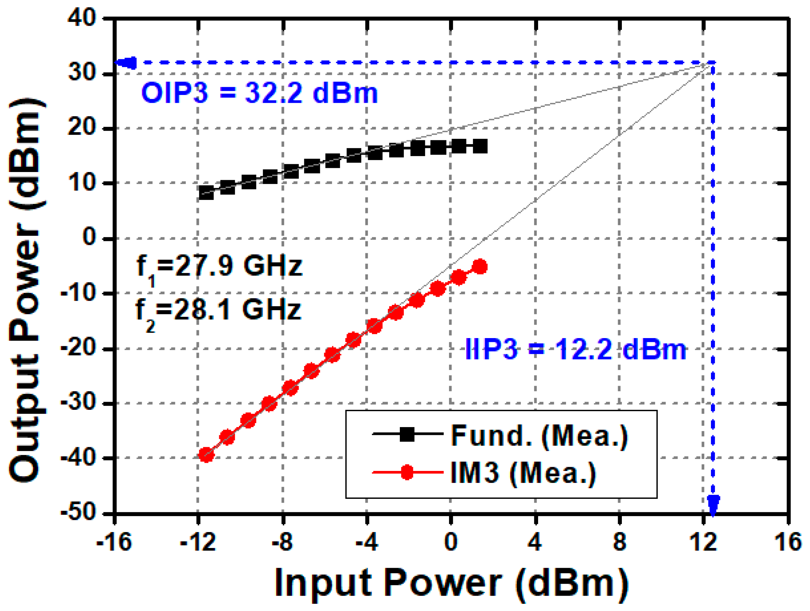
4. Experimental Result

The proposed 26–30 GHz GaN HEMT LNA MMIC that adopts the series inductor-based stability enhancement technique was fabricated using 0.15-μm GaN-on-SiC technology, and its performance was demonstrated from bare-die measurements. Figure 8 shows a die microphotograph of the implemented design, which occupies an active area of 2.61 mm × 1.02 mm (2.66 mm2), including bonding pads. All test measurements were conducted using a single die via on-wafer probing. RF signals were injected externally and measured at the RF input and output ports, respectively, using GSG-type probes, whereas the required gate and drain bias voltages were supplied through GPPPG-type DC probes. The overall insertion loss arising from the cables and probes was measured at the desired frequencies and used to compensate for the measured results. Figure 9 shows the measurement setups for the S-parameter, NF, and linearity performance characterization, focusing on band n257 and band n261 of the 5G NR FR2.
Figure 10 shows the measured and simulated S-parameter results, which include the small-signal gains (S21s) and input and output return losses (S11s and S22s). The designed LNA achieves a maximum small-signal gain of 20.2 dB with a 1-dB bandwidth of approximately 7 GHz (23.6–30.3 GHz). As is also seen from Figure 10, a gain degradation of 2–3 dB is observed in comparison with the simulation results. This is mainly caused by a slight deviation from the optimal matching condition. The attained return loss results are less than –10 dB over the 26–30 GHz frequency range.
To primarily validate the stability performance improvement of the designed LNA over the frequency range, μ values were calculated from the measured S-parameter values, and the results are presented in Figure 11 along with the simulated μ values. It is noted that μ enhancement is achieved with the peak value of μ = 7.68 at 27.6 GHz, even if the peak frequency is slightly shifted to a lower frequency in comparison with the simulated stability results. Moreover, the designed LNA with the stability enhancement technique achieves an unconditionally solid stable condition, where μ is greater than 1 over the frequency range of 20–35 GHz. The measured and simulated NFs of the designed LNA, shown in Figure 12, range from 2.42 to 2.56 and 1.5 to 1.6 dB, respectively, in the operating frequency. The measured NFs of the implemented design are approximately 0.9 dB higher than the simulated NFs owing to the degraded small-signal gain and deviated noise-matching condition.
In addition, the performance of an in-band (IB) output 1-dB compression point (OP1dB) and output-referred third-order intercept point (OIP3) were investigated at fRF (fRF = 28 GHz) to demonstrate the excellent power handling capability of the designed GaN HEMT LNA MMIC. Figure 13 shows the in-band (IB) P1dB obtained by measuring output tone power values and small-signal gains with respect to the applied input tone power values at fRF. The evaluated OP1dB is approximately 17.2 dBm. This indicates that the gain compression mainly occurs at the output of the design. Moreover, the OIP3 performance was characterized by IB two tones at f1 and f2 (f1 = fRF + 20 MHz and f2 = fRF + 40 MHz). The attained fundamental and third-order intermodulation (IM3) product tones versus the input IB tone power are shown in Figure 14, and the evaluated OPI3 was approximately 32.2 dBm.
A comparison of the measured performance metrics of the proposed LNA with those of state-of-the-art GaN HEMT LNA MMIC is presented in Table 3. As can be seen from Table 3, the obtained performance of the proposed design, which adopts series inductors is better or comparable to that of other designs for the given power consumption with noticeable stability enhancement.

5. Conclusions

We presented a three-stage GaN HEMT LNA MMIC based on the 0.15-μm GaN-on-SiC technology, for use in 5G NR FR2 base station applications, for the frequency range of 26–30 GHz. In this design, it was demonstrated that adopting a series inductor between the stages enhances the stability performance with minimum degradation of the small-signal gain and NF performance, specifically at the operating frequency. Through performance verification of the implemented design, it was ensured that the series-inductor-based technique could be successfully utilized in the GaN HEMT design to improve the gain and stability performance.

Author Contributions

Conceptualization, H.A., H.J., D.K., S.L., and J.H.; methodology, H.A., H.J., D.K., S.L., and J.H.; validation, H.A., H.J., S.-M.S., and J.H.; data curation, H.A., H.J. and S.-M.S.; writing—original draft preparation, H.A. and J.H.; writing—review and editing, H.J., D.K., S.L.; funding acquisition, J.H. All authors have read and agreed to the published version of the manuscript.

Funding

This research was supported in part by the Institute for Information and communications Technology Planning (IITP) grant funded by the Ministry of Science and ICT (2020-0-00158-001) and in part by the Regional Innovation Strategy (RIS) through the National Research Foundation of Korea (NRF) funded by the Ministry of Education (MOE) (2021RIS-004).

Institutional Review Board Statement

Not applicable.

Informed Consent Statement

Not applicable.

Data Availability Statement

Not applicable.

Acknowledgments

The authors would like to thank J. Jung of ICT Creative Research Lab, Electronics and Telecommunication Research Institute (ETRI) for their assistance with measurement equipment.

Conflicts of Interest

The authors declare no conflict of interest.

References

  1. Standard TS 38.101 V15.8.0, 3GPP; Specification Group Radio Access Network NR. User Equipment (UE) Radio Transmission and Reception—Part 1: Range 1 Standalone (Release 15). ETSI: Sophia-Antipolis, France, 2020.
  2. Hossain, E.; Hasan, M. 5G cellular: Key enabling technologies and research challenges. IEEE Instrum. Meas. Mag. 2015, 18, 11–21. [Google Scholar] [CrossRef]
  3. Shinjo, S.; Nakatani, K.; Tsutsumi, K.; Nakamizo, H. Integrating the front end: A highly integrated RF front end for high-SHF wide-band massive MIMO in 5G. IEEE Microw. Mag. 2017, 18, 31–40. [Google Scholar] [CrossRef]
  4. Balteanu, F.; Modi, H.; Choi, Y.; Lee, J.; Drogi, S.; Khesbak, S. 5G RF front end module architectures for mobile applications. In Proceedings of the 2019 49th European Microwave Conference (EuMC), Paris, France, 1–3 October 2019. [Google Scholar]
  5. Pengelly, R.S.; Wood, S.M.; Milligan, J.W.; Sheppard, S.T.; Pribble, W.L. A review of GaN on SiC high electron-mobility power transistors and MMICs. IEEE Trans. Microw. Theory Tech. 2012, 60, 1764–1783. [Google Scholar] [CrossRef]
  6. Yeom, K.W. Microwave Circuit Design: A Practical Approach Using ADS; Prentice Hall: Ann Arbor, MI, USA, 2015; pp. 356–357. [Google Scholar]
  7. Golio, M. RF and Microwave Semiconductor Handbook; CRC Press: Boca Raton, FL, USA, 2003. [Google Scholar]
  8. Lv, G.; Chen, W.; Liu, X.; Feng, Z. A dual-band GaN MMIC power amplifier with hybrid operating modes for 5G application. IEEE Microw. Wirel. Compon. Lett. 2019, 29, 228–230. [Google Scholar] [CrossRef]
  9. Nakatanim, K.; Yamaguchi, Y.; Komatsuzaki, Y.; Shinjo, S. Millimeter-wave GaN power amplifier MMICs for 5G Application. In Proceedings of the IEEE International Symposium on Circuits and Systems (ISCAS), Sapporo, Japan, 26–29 May 2019. [Google Scholar]
  10. Cheng, P.; Wang, Q.; Li, W.; Jia, Y.; Liu, Z.; Feng, C.; Jiang, L.; Xiao, H.; Wang, X. A Broadband Asymmetrical GaN MMIC Doherty Power Amplifier with Compact Size for 5G Communications. Electronics 2021, 10, 311. [Google Scholar] [CrossRef]
  11. Hu, L.; Liao, X.; Zhang, F.; Wu, H.; Ma, S.; Lin, Q.; Tang, X. A Wideband High-Efficiency GaN MMIC Power Amplifier for Sub-6-GHz Applications. Micromachines 2022, 13, 793. [Google Scholar] [CrossRef] [PubMed]
  12. Curtis, J.; Zhou, H.; Aryanfar, F. A fully integrated Ka-band front end for 5G transceiver. In Proceedings of the IEEE MTT-S International Microwave Symposium (IMS), San Francisco, CA, USA, 22–27 May 2016. [Google Scholar]
  13. Ahn, H.J.; Chang, W.I.; Kim, S.M.; Park, B.J.; Yook, J.M.; Eo, Y.S. 28 GHz GaAs pHEMT MMICs and RF front-end module for 5G communication systems. Microw. Opt. Technol. Lett. 2019, 61, 878–882. [Google Scholar] [CrossRef]
  14. Erofeev, E.; Arykov, V.; Stepanenko, M.; Voevodin, A.; Kogai, A.; Kurikalov, V. 28 GHz single-chip transmit RF front-end MMIC for multichannel 5G wireless communications. Symmetry 2020, 12, 1167. [Google Scholar] [CrossRef]
  15. Park, J.; Kim, J.-G. A 28 GHz GaAs front-end IC with single positive supply voltage. Microw. Opt. Technol. Lett. 2021, 63, 1171–1176. [Google Scholar] [CrossRef]
  16. Schuh, P.; Sledzik, H.; Reber, R. GaN-based single-chip frontend for next-generation X-band AESA systems. Int. J. Microw. Wirel. Technol. 2018, 10, 660–665. [Google Scholar] [CrossRef] [Green Version]
  17. Suijker, E.M.; Rodenburg, M.; Hoogland, J.A.; Heijningen, M.; Seelmann-Eggebert, M.; Quay, R.; Bruckner, P.; Vliet, F.E. Robust AlGaN/GaN low noise amplifier MMICs for C-, Ku- and Ka-band space applications. In Proceedings of the IEEE Compound Semiconductor Integrated Circuit Symposium (CSICS), Greensboro, NC, USA, 11–14 October 2009. [Google Scholar]
  18. Rudolph, M.; Chaturvedi, N.; Hirche, K.; Wurfl, J.; Heinrich, W.; Trankle, G. Highly rugged 30 GHz GaN low-noise amplifiers. IEEE Microw. Wirel. Compon. Lett. 2009, 19, 251–253. [Google Scholar] [CrossRef]
  19. Micovic, M.; Brown, D.; Regan, D.; Wong, J.; Tai, J.; Kurdoghlian, A.; Herrault, F.; Tang, Y.; Burnham, S.D.; Fung, H.; et al. Ka-band LNA MMIC’s realized in fmax > 580 GHz GaN HEMT technology. In Proceedings of the IEEE Compound Semiconductor Integrated Circuit Symposium (CSICS), Austin, TX, USA, 23–26 October 2016. [Google Scholar]
  20. Nguyen, H.H.; Luong, D.M.; Bach, G.D. A novel independently biased 3-Stack GaN HEMT configuration for efficient design of microwave amplifiers. Appl. Sci. 2019, 9, 1510. [Google Scholar] [CrossRef]
  21. Pace, L.; Colangeli, S.; Ciccognani, W.; Longhi, P.E.; Limiti, E.; Leblanc, R.; Feudale, M.; Vitobello, F. Design and validation of 100 nm GaN-On-Si Ka-Band LNA based on custom noise and small signal models. Electronics 2020, 9, 150. [Google Scholar] [CrossRef]
  22. Tong, X.; Zhang, L.; Zheng, P.; Zhang, S.; Xu, J.; Wang, R. An 18–56-GHz wideband GaN low-noise amplifier with 2.2–4.4-dB noise figure. IEEE Microw. Wirel. Compon. Lett. 2020, 30, 1153–1156. [Google Scholar] [CrossRef]
  23. Florian, C.; Traverso, P.A.; Santarelli, A. A Ka-band MMIC LNA in GaN-on-Si 100-nm technology for high dynamic range radar receivers. IEEE Microw. Wirel. Compon. Lett. 2021, 31, 161–164. [Google Scholar] [CrossRef]
  24. Parveg, D.; Varonen, M.; Kantanen, K. A full Ka-band GaN-on-Si low-noise amplifier. In Proceedings of the IEEE 2020 50th European Microwave Conference (EuMC), Utrecht, The Netherlands, 12–14 January 2021. [Google Scholar]
  25. Edwards, M.L.; Sinsky, J.H. A new criterion for linear 2-port stability using a single geometrically derived parameter. IEEE Trans. Microw. Theory Tech. 1992, 40, 2303–2311. [Google Scholar] [CrossRef]
  26. Pozar, D.M. Microwave Engineering, 4th ed.; John Wiley & Sons Inc.: Hoboken, NJ, USA, 2012; p. 567. [Google Scholar]
Figure 1. Front-end module configuration using (a) GaAs and (b) GaN technologies [16].
Electronics 11 02716 g001
Figure 2. Stability enhancement configurations: (a) a cascode stage, (b) a single stage with source degeneration, and (c) a single stage with an output series resistor.
Electronics 11 02716 g002
Figure 3. Common source single stage (4F25) adopting series inductor-based stability enhancement technique.
Electronics 11 02716 g003
Figure 4. Simulation results of the common-source single stage adopting series inductor: (a) a S12 and (b) a stability μ criterion.
Electronics 11 02716 g004
Figure 5. Single-stage common-source GaN HEMT-based amplifier configuration (4F25) (a) with a series inductor at the drain node and (b) with series inductors at both gate and drain nodes.
Electronics 11 02716 g005
Figure 6. Simulated performance of the single-stage common-source GaN HEMT-based amplifier configuration with different values of series inductors at the drain node (output) (Figure 5a) and at both gate and drain nodes (input and output) (Figure 5b); (a) stability μ criteria, (b) small-signal gains (S21s), and (c) noise figures.
Electronics 11 02716 g006aElectronics 11 02716 g006b
Figure 7. Schematic of the designed three-stage GaN low-noise amplifier employing inductor-based stability enhancement technique.
Electronics 11 02716 g007
Figure 8. Die microphotograph of the implemented GaN HEMT-based low-noise amplifier.
Electronics 11 02716 g008
Figure 9. Measurement configurations: (a) a block diagram of the S-parameter, noise figure, P1dB, and IIP3 performance measurements and (b) a probe station setup.
Electronics 11 02716 g009aElectronics 11 02716 g009b
Figure 10. Measured and simulated small signal gains, S11s and S22s of the LNA.
Electronics 11 02716 g010
Figure 11. Measured and simulated stability μ values of the LNA.
Electronics 11 02716 g011
Figure 12. Measured and simulated NFs of the LNA.
Electronics 11 02716 g012
Figure 13. Measured IB OP1dB performance at fRF (fRF = 28 GHz). Black dot: Fund. Red dot: IM3.
Electronics 11 02716 g013
Figure 14. Measured IB OIP3 performance with f1 = fRF + 20 MHz and f2 = fRF + 40 MHz.
Electronics 11 02716 g014
Table 1. Comparison of the material properties of various microwave semiconductors.
PropertySiGaAsInPSiCGaN
Energy bandgap, Eg (eV)1.121.421.343.23.44
Breakdown field, Eb (106 V/cm)0.30.40.63.22
Saturation velocity (105 m/sec)11.21.02.02.5
Dielectric constant, ε11.712.912.4109.5
Electron mobility, μ (cm2/V·S)1450850046007001600
Thermal conductivity (W/cm°K)1.310.460.774.91.5
B-FOM ratio 1113.175.769.6225.96
1 B-FOM: Baliga’s figure-of-merit, defined as ε·μ·Eg3.
Table 2. Values of the utilized components.
ComponentsValuesComponentsValues
LSE510 pHCB13.16 pF
RG202 ΩCB20.56 pF
RB202 ΩCBLK0.36 pF
WTL15 μmLS1, LS2, LS3130 μm
LIN1250 μmLIN2280 μm
LINT1160 μmLINT2240 μm
LINT3176 μmLINT4860 μm
LOUT1120 μmLOUT2459 μm
Table 3. Performance summary and comparison with previously reported work.
ReferenceThis Work[17][24][18][21][23]
Frequency
(GHz)
26–3026–3126–4027–3134–37.533–38
Gain
(dB)
20.218.9–24.5>2314.4–19.63125–26
S11/S22
(dB)
<–10/<–10–12.5/<–6.5<–5/<–10<–5/<–10<–8/<–10≥10
NF
(dB)
2.42–2.564–51.7–2.73.7–3.92.4–2.62.0–2.2
OP1dB
(dBm)
17.212.512–22NA2320
OIP3
(dBm)
32.2NA20–32NA3228.4
Stability 1
(μ)
Uncon. Stable
(Up to 7.7)
NAUncon. Stable
(Up to ~9)
Uncon. Stable
(NA)
Uncon. Stable
(NA)
NA
Power
(W)
0.32NA0.430.561.3NA
Chip Size 22.666NA4.087.25.5
Process0.15-μm
GaN-on-SiC
0.15-μm
GaN-on-SiC
0.1-μm
GaN-on-Si
0.15-μm
GaN-on-SiC
0.1-μm
GaN-on-Si
0.1-μm
GaN-on-Si
1. NA: Not Available. 2. Including bonding pads.
Publisher’s Note: MDPI stays neutral with regard to jurisdictional claims in published maps and institutional affiliations.

