Article

Substrate-Induced Dissipative and Non-Linear Effects in RF Switches: Probing Ultimate Performance Based on Laser-Machined Membrane Suspension

1
Univ. Lille, CNRS, Centrale Lille, Junia, Univ. Polytechnique Hauts-de-France, UMR 8520–IEMN–Institut d’Electronique, de Microélectronique et de Nanotechnologie, 59000 Lille, France
2
STMicrolectronics, 38926 Crolles, France
*
Author to whom correspondence should be addressed.
Electronics 2022, 11(15), 2333; https://doi.org/10.3390/electronics11152333
Submission received: 23 May 2022 / Revised: 11 July 2022 / Accepted: 25 July 2022 / Published: 27 July 2022
(This article belongs to the Special Issue RF/Microwave Circuits for 5G and Beyond)

Abstract

:
With the evolution of radio frequency (RF)/microwave technology, there is a demand for circuits that are able to meet highly challenging RF front end specifications. Silicon-on-insulator (SOI) technology is one of the leading platforms for upcoming wireless generation. The degradation of performance due to substrate coupling is a key problem to address for telecommunication circuits, especially for the high throw count switches in RF front ends. In this context, a fast, flexible and local laser ablation technique of the silicon handler allows for the membrane suspension of large millimeter-scale circuits. This approach enables the evaluation of the ultimate performance in the absence of the substrate, i.e., without dissipative losses and substrate-induced non-linear effects, on capacitive comb coupling structures and RF switches. Compared to high-resistivity SOI substrates, the high frequency characterization of RF membrane switches reveals a superior linearity performance with a reduction in second and third harmonics by 17.7 dB and 7.8 dB, respectively. S-parameter analysis also reveals that membrane suspension entails insertion losses that are improved by 0.38 dB and signal reflection lowered by 4 dB due to a reduced off-state capacitance. With reference to a trap-rich substrate, the membrane suspension also achieves an additional 7.8 dB reduction in the second harmonic, indicating that there is still scope for improvement in this figure of merit. The obtained results demonstrate a new way to evaluate optimized circuit performance using post-fabrication substrate engineering.

1. Introduction

Radiofrequency (RF) front ends are constantly evolving to support new communication standards, leading to increasingly more stringent specifications in terms of loss and linearity. As a result, RF designers continually need technology options to meet these challenging specifications. RF switches are important components of the RF front end as they allow the selective propagation of the signal through transmit/receive pathways using antenna swapping, power and diversity switches to accommodate the increasing number of communication standards. There is a demand for high throw count switches in order to be able to support the integration of different communication standards such as GSM, TD-SCDMA, WCDMA and LTE within the same chip [1]. Another example of the demanding use of switches is given by carrier aggregation (CA), which is a key feature of the LTE-advanced and 5G standards. CA imposes extremely tight new specifications in terms of operational bandwidth, insertion loss, isolation, linearity and power handling [2]. Traditionally, GaAs p-HEMT and silicon-on-sapphire technologies have been preferred for switch design due to their superior substrate isolation [3,4], which was not possible on silicon. The introduction of high-resistivity SOI with substrate resistivity greater than 1 kΩ.cm was a breakthrough for the flourishing of RF technology on SOI. A large number of switch designs have been reported ever since and a few examples are reported in [5,6,7,8]. The innovation in SOI has led to the development of two types of wafers: high-resistivity SOI (HR-SOI) and trap-rich SOI (TR-SOI). In the former, despite a bulk substrate resistivity greater than 1 kΩ·cm, a parasitic surface conduction layer (PSC) [9,10] is formed at the interface between the buried oxide (BOX) and the silicon (Si) handler. This thin layer of locally enhanced conductivity contributes to substrate-related losses and non-linearity. In the latter, this effect is mitigated by the introduction of a polysilicon layer naturally rich in trap states, which strongly pin the potential and prevents the formation of a parasitic conduction layer. The trap-rich layer greatly improves the loss and linearity figures of circuits as has been shown in [11,12,13]. Despite significant improvements in SOI wafer technology, substrate coupling still occurs, and degradation in performance is not negligible, especially for bulky circuits such as RF power switches. Improving the performance of switches has profound implications for the whole RF front end. Cutting the switch losses by 0.1 dB can improve the front end Tx efficiency by 1%, and this improvement in efficiency takes around two years [14]. Substrate coupling increases the overall capacitance of the OFF branches, which leads to losses and a degraded Ron × Coff figure of merit (FoM) [15]. Additionally, the parasitic substrate impedance is a source of the non-linear behavior of the switch [16]. Thus, it is desirable to mitigate the substrate effects as shown in previous works where the removal of handler substrate has proved to offer multiple benefits for different kinds of RF circuits [17,18,19,20,21,22]. In the aforementioned studies, the handler substrate is replaced with another host substrate, plastic or glass, with reduced losses when compared to silicon. While there are improvements, the fabrication processes are cumbersome, and substrate effects are not brought to a minimum due to the presence of the host substrate attached to the BOX by means of a bonding material.
In this work, we cross a distinctive milestone in substrate optimization. We report, for the first time to our knowledge, a methodology based on fast laser ablation to locally suspend mm-sized RF devices/circuits with the silicon handler locally removed. After processing, only a membrane a few micrometers thick remains in place, consisting of the BOX, the active silicon layer and the interconnection network, which represents the ultimate minimal layer stack beyond which the electrical functionality cannot be preserved. The local suspension methodology is based on the use of a focused laser beam in order to perform a precise ablation to control the extracted volume of silicon and the roughness of the remaining material. For this purpose, a pulsed laser source is used to take advantage of the fascinating light–matter interaction mechanisms associated to a focused beam [23]. For instance, in the femtosecond pulse regime and for a fluence close to the ablation threshold, non-linear absorption is responsible for laser micromachining of silicon even in near infrared for which silicon is transparent under ordinary conditions [24]. Femtosecond laser processing is therefore utilized to etch handler silicon locally, which fully eliminates substrate parasitics, leading to enhanced RF circuits. This powerful, flexible and post-process short-loop technique is applied here to two test vehicles to quantify the impact of the substrate on RF performance in the linear and non-linear regimes. The first is a test structure composed of two interleaved combs on the first interconnect level to study the parasitic coupling through the substrate in the small signal regime. The second is a single-pole-9-throw (SP9T) switch test structure designed to evaluate second and third harmonics’ generation in a demanding use case where one of the channels is passing with the other eight in the blocked state. In the latter case, the sub-6 GHz frequency range is addressed, which is of interest for 5G applications [25]. It is emphasized here that although membrane suspension of devices/circuits by laser micromachining may not be a relevant technique for mass production, the objective of this paper is to probe the ultimate margins of performance gain achievable in the absence of a silicon handler and to position the HR and TR substrates with respect to a suspended membrane free of substrate-induced dissipative and non-linear effects. This paper is organized as follows. A laser-assisted substrate removal process is briefly described in Section 2. To quantitatively study parasitic substrate coupling in terms of losses, RF characterization of capacitive coupling combs is first reported in Section 3. Finally, the performance of RF switch membranes are compared with HR-SOI and TR-SOI substrate types in Section 4.

2. Laser-Assisted Substrate Removal

The key step for the fabrication of membranes of switches is femtosecond laser ablation. A schematic explanation of the process is given in Figure 1. A focused laser beam is scanned in a serpentine fashion as shown in Figure 1b to ablate material within the area covered by the laser scan. Laser ablation is not uniform and ablated surfaces have finite roughness. Hence, laser ablation alone is not sufficient to remove material up to the BOX as such an attempt would result in unwanted etching of the oxide layer in some local areas. Laser ablation is therefore performed until the remaining thickness of silicon is a few tens of microns. The ablated cavities are then subject to a xenon difluoride (XeF2) vapor etching step. XeF2 is a highly selective etchant of Si over SiO2 with a selectivity ratio of ~1000:1.
The areas of the die that are not to be etched are protected by a protective dry film (Ajinomoto GX-T31). Etching is performed over multiple cycles. In each cycle, XeF2 gas is introduced into the chamber at a pressure of 2–3 Torr for a time period of 10–15 s and it is vented out at the end of each cycle. About 25–100 cycles of etch are needed depending on the thickness of the silicon to be etched to completely remove the handler silicon in the ablated area to obtain membranes of circuits suspended on the BOX. The laser ablation process, also referred to as FLAME (Femtosecond Laser-Assisted Micromachining and Etching), is fully detailed in [26,27]. A high removal rate of up to 8.5 × 106 µm3 s−1 is obtained by optimized laser milling parameters. The process is designed to retain handler silicon under RF pads to withstand the mechanical forces applied during contact probing on the pads. The thickness of handler silicon under the pads is also reduced to a few tens of microns at the end of the process.

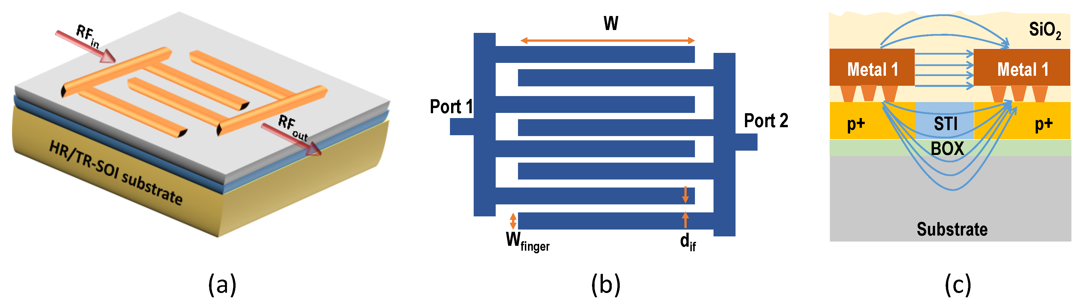
3. Capacitive Comb Coupling Structure

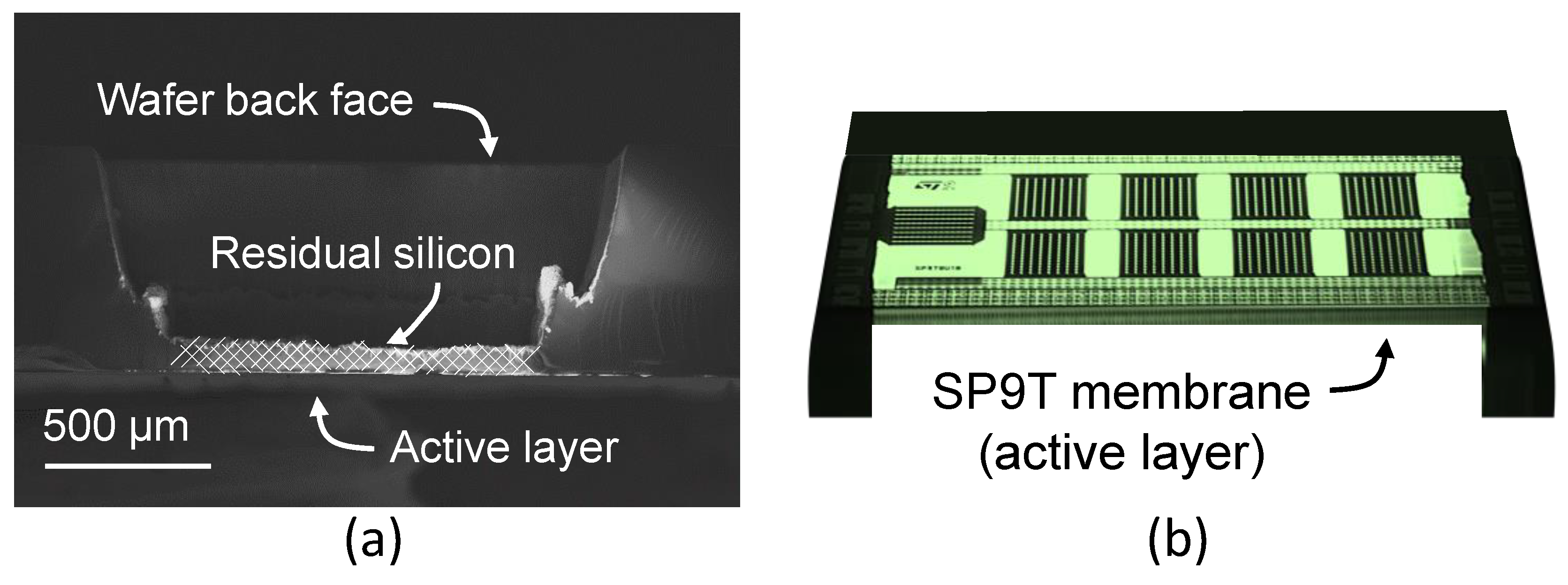
3.1. Device Structure and Post-Processing

Capacitive coupling structures are fabricated based on the 130 nm H9SOIFEM process technology by STMicroelectronics [28]. This technology combines a 180-nm-thick SOI film and a 400-nm-thick BOX layer. These structures are specially designed to study and quantify the effect of substrate coupling in RF circuits. They also serve to demonstrate if membranes of circuit stacks can be reliably fabricated. A schematic illustration of these structures is shown in Figure 2. They contain long interdigitated fingers separated by a defined spacing. The fingers start from metal 1 and they are contacted to the active silicon, which is p+ doped. The fingers are separated by a shallow trench isolation (STI) as shown in Figure 2c. The interdigitated structures are connected to RF pads on either side, which allows two-port RF measurements. When an RF signal is sent from one side, coupling takes place both through the layers above the BOX as well as through the substrate.
Two versions of the coupling structures are characterized: CPL-A and CPL-B. The different dimensions of the comb structures are listed in Table 1. The difference between the two structures lies in the number of fingers and the spacing between them. CPL-A has fewer fingers with higher spacing, while CPL-B has a higher number of fingers with smaller spacing. After application of the FLAME post-processing step as described in the previous paragraph, the suspended membrane is visualized using dual-light microscopy (DLM) where both the front side and back side are illuminated with varying intensities. The high intensity backlight through the cavity appears brighter in the microscope image outlining the area of the membrane. The DLM images for CPL-A and CPL-B are shown in Figure 3. It can be seen that bulb-like features appear at some places around the outline of the membrane. These bulb-like features are a result of the uneven local etching characteristic of XeF2. Some places have an enhanced etch rate in the lateral direction as compared to the others. These features can be avoided by fine-tuning the process in order to have fewer cycles of XeF2 etching.

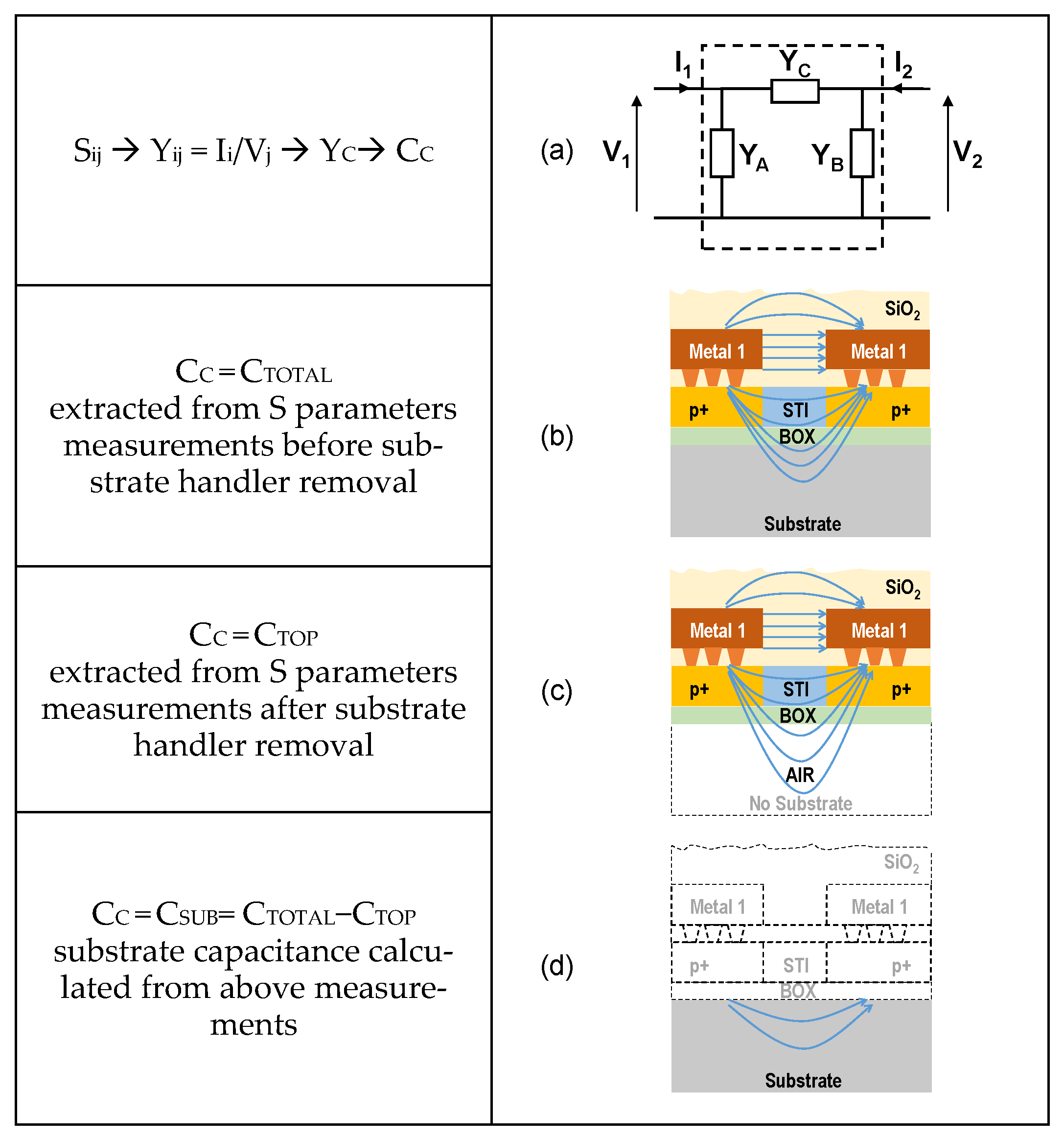
3.2. Extraction of the Substrate Coupling Contribution

Two-port S-parameter characterization is performed over a frequency range of 20 MHz to 26 GHz. The measurements are performed using a Rohde & Schwarz ZVA 67 vector network analyzer, and Infinity probes (GSG type) from Cascade Microtech are used to make contact with the RF pads on the die. The substrate is also DC-biased through the chuck. S-parameter measurements are performed for different substrate bias conditions covering the −2.5 V to +2.5 V range. In this study, the lateral capacitive coupling occurring between the two ports is the parameter of interest. In order to extract this figure, the measured parameters Sij are converted into an admittance matrix Yij and then identified with the model shown in Figure 4a involving three admittances associated in a π-type configuration. From this identification, it follows that the admittance YC representing the lateral coupling can be discriminated from the admittances YA and YB that integrate parasitic capacitances associated with the measurement pads. It is thus possible to deduce the coupling capacitance CC between the two interdigitated electrode combs as reflected by the following relationships
Y = [ Y A + Y C Y C Y C Y B + Y C ]
C c = i m a g ( Y C ω ) = i m a g ( Y 12 ω ) = i m a g ( Y 21 ω )
The following methodology was applied to assess the role of lateral electric field coupling through the substrate, which is a well-established source of dissipative loss:
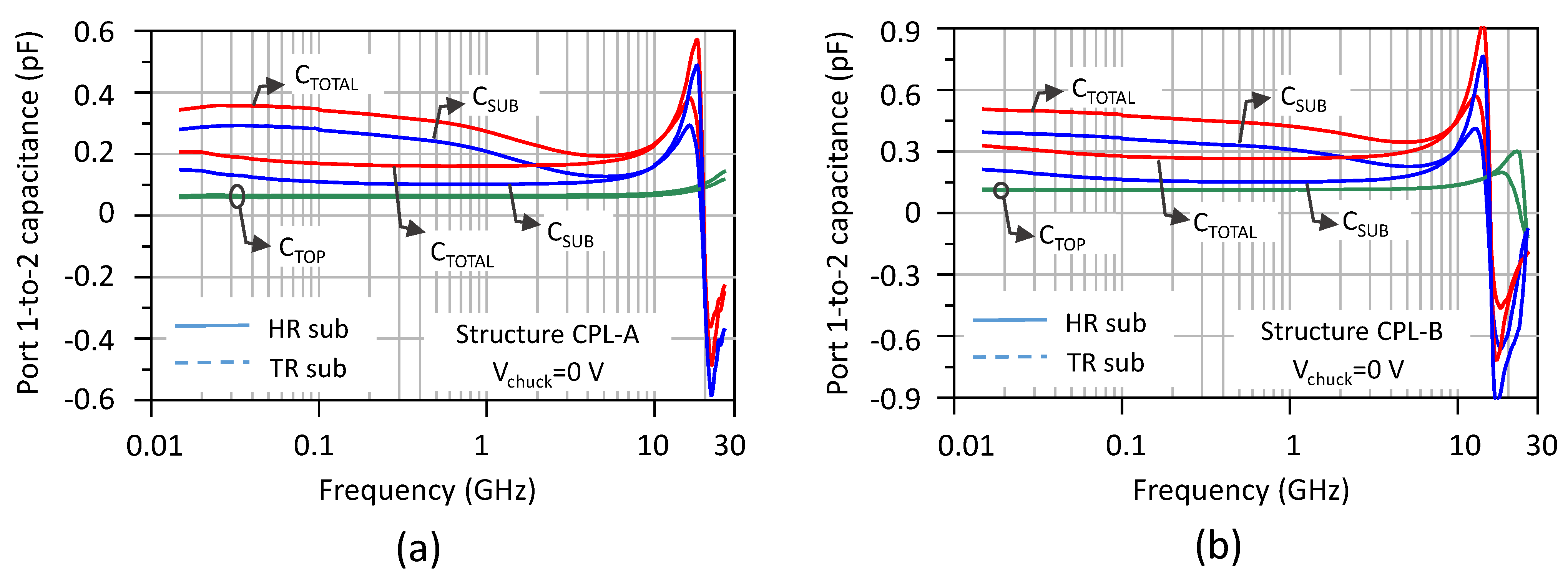
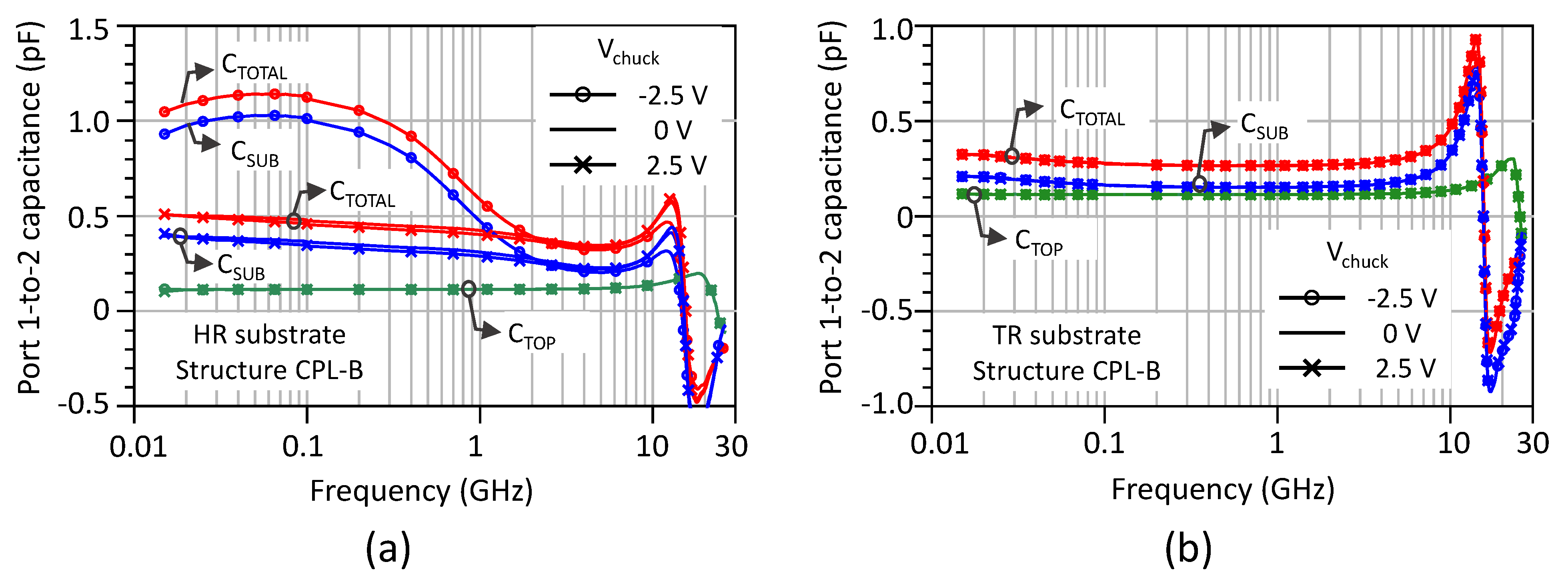
  • S-parameter measurements are first performed on a structure with an unmodified substrate. From this step, the evaluation of the total CTOTAL capacitance is obtained as shown in Figure 4b
  • After the local removal of the substrate down to the BOX, a second sequence of S-parameter measurements is used to extract the CTOP capacitance, which mainly reflects the electrostatic coupling introduced by the metal combs belonging to the back-end of line interconnects (Figure 4c)
  • Finally, the substrate capacitance CSUB is deduced from the previous measurements, considering that CTOP and CSUB are associated in parallel to yield the total capacitance CTOTAL (Figure 4d).
In the above methodology, it is worth noting that the relation CSUB = CTOTAL−CTOP is not exactly valid. When the silicon is locally removed (Figure 4c), the electric field lines through the air below the chip constitute a fringe contribution, which is neglected here. In reality, the fringe field lines in the air are involved in an attenuated manner in a proportion which is that of the ratio of the dielectric permittivities, i.e., ~1(air)/11.7(silicon). In this sense, CTOP is slightly overestimated and, consequently, CSUB is underestimated. As the permittivity ratio is in the order of 8.5%, the conclusions on the relative contribution of the substrate to the total capacity for the HR and TR substrates remain valid in very good approximation.
Figure 5 shows the variations in the different capacitance components as a function of frequency for the two types of starting substrates HR and TR. The chuck bias is here kept grounded. Overall, the capacitance values of the CPL-A structure (Figure 5a) are lower than those of CPL-B (Figure 5b) as expected due to a smaller finger gap and number of fingers. It is worth noting that these structures are resonant devices that behave as a capacitance at low frequency and are ultimately dominated by a parasitic inductance in the high frequency range. This is exactly the opposite situation compared to suspended integrated coil inductances, where the dominant influence of capacitive coupling occurs above the resonance frequency [29]. In the following discussion, we limit the analysis to the frequency range reflecting only capacitive coupling, i.e., below the resonant frequency, which occurs around 15 GHz. A close examination of Figure 5 reveals two points of particular interest:
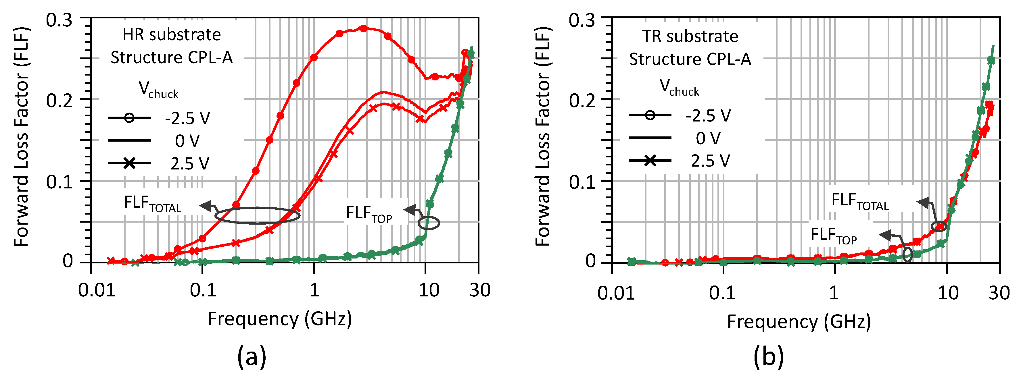
  • Firstly, the substrate makes a substantial contribution to the total capacitance for both types of substrates even though its relative importance is lesser in the TR case.
  • Secondly, CTOP is the same regardless of the initial substrate, HR or TR. As this capacitance is measured after local removal of the substrate, this result is expected and verified, and validates the method of the dissociation of capacitive contributions detailed in Figure 4. It can also be noted that CTOP remains strictly flat and frequency-independent, as one would expect from an insulating dielectric material free of any space charge.
It is important to note that the stack consisting of the doped SOI film, the buried oxide and the silicon handler forms a MOS capacitor. On unprocessed structures, it is therefore expected that a depletion region as well as a parasitic surface conduction layer (PSC), here in inversion, will develop under the buried oxide when the chuck bias is negative because the substrate is p-type. To this end, Figure 6 provides a deeper insight by considering the frequency-dependent capacitive coupling for various chuck biases (Vchuck) applied to the backside of the substrate handler. In the case of the HR substrate, Figure 6a shows the impact of the depletion effect for a chuck bias of −2.5 V. A significant increase in CSUB and CTOTAL at low frequencies can be understood by considering that any extension in depth of the depletion region increases the cross-sectional area of the capacitance that connects the electrodes of the combs. A marked dependence of CTOTAL and CSUB upon frequency is observed between 200 MHz and 2 GHz, followed by a convergence to the same values as those obtained at VSUB = 0 and 2.5 V.
This convergence at 2 GHz can be attributed to the charge dynamics of majority carriers, which become limited by dielectric relaxation. The dielectric relaxation time (τd) is given by the product of the dielectric constant and the resistivity of the substrate. For the sake of illustration, τd is typically equal to ~0.5 ns, which corresponds to a frequency of 2 GHz for a high-resistivity substrate of 0.5 kΩ·cm. Under these conditions, the transport of majority carriers is impacted by an inertia effect, which no longer allows carriers to respond fast enough to a high-frequency excitation. For the other bias conditions (0 and 2.5 V), the small extension of the depletion region or the absence of the PSC layer leads to the same lower value of the lateral capacitance, which becomes quasi-independent of bias and frequency. For coupling structures initially fabricated on a TR-SOI substrate, Figure 6b shows that all capacitance components remain almost perfectly flat with frequency and independent of chuck bias. This behavior is naturally expected for CTOP, which is measured after local substrate removal. A comparison with Figure 6a also confirms that CTOP is the same (~0.11 pF) on the flat portion of the curves below resonance regardless of the starting substrate and bias. The remarkable property inherited from the TR substrate is that CSUB, and in turn CTOTAL, remain quasi-constant as a function of frequency and independent of the chuck bias. This behavior is attributed to the strong pinning of the Fermi level due to the high density of charged states in the polysilicon trap-rich layer. Its presence creates an equipotential plane under the buried oxide and therefore tends to verticalize the electric field lines because equipotential planes and electric field lines are orthogonal. In this sense, the presence of the trap-rich layer leads to the decrease in lateral electrostatic coupling observed in Figure 6b.

3.3. Substrate Dissipation Losses

Figure 7 shows the forward loss factor FLF = 1−|S11|2−|S21|2 of the CPL-A structure for both types of substrate and various chuck biases. Prior to substrate removal, the integrated coupling structures on the HR substrate (Figure 7a) exhibit substantial losses (FLFTOTAL), the levels of which are exacerbated by the depletion state and the formation of a PSC layer below the buried oxide at Vchuck = −2.5 V. After membrane suspension, losses (FLFTOP) are considerably reduced and become independent of bias because of the replacement of handler silicon by air. It is recalled here that our analysis is restrained to the frequency range below resonance that reflects capacitance coupling. The same information is provided for the TR substrate in Figure 7b. It is interesting to note that the losses before removal of the TR substrate are strongly reduced and independent of Vchuck due to the potential pinning effect of the trap-rich layer. The variations in FLFTOP show that the membrane suspension provides a further reduction in substrate dissipative losses. In the end, the results in Figure 6b show that while the TR substrate still contributes significantly to the lateral capacitive coupling between the metal electrodes of the comb, its behaviour is that of an almost lossless dielectric material from the RF point of view as outlined in Figure 7b. While the studied comb structures are particularly suitable for exacerbating capacitive coupling, they also quantify the role of the substrate in the level of isolation and crosstalk. In order to compare the isolation performance before and after application of the FLAME process, the difference in isolation efficiency ΔS21(HR/TR) = S21(HR/TR)−S21(SR) (dB), where the subscript SR refers to ‘substrate removed’, is calculated for CPL-A and CPL-B at a chuck bias of 0 V and is reported in Table 2. Up to 100 MHz, the difference in isolation ΔS21(HR) is greater than 13 dB in the HR substrate case for both comb structures. The difference ΔS21(TR) is smaller for the TR-SOI substrate with values of 10.7 dB and 8.9 dB for CPL-A and CPL-B, respectively, at 20 MHz. At operating frequencies of practical interest such as 5 GHz, the isolation improvement provided by the membrane suspension remains significant. However, for a chuck bias of 0 V, the enhancement amounts to ΔS21 (HR) = 6.8 dB and ΔS21 (TR) = 7.5 dB for CPL-A. For the CPL-B structure, we obtain the same non-negligible figure ΔS21(HR) = ΔS21(TR) = 5.2 dB associated to the HR and TR substrates.
By extracting the capacitances of membrane-suspended comb structures, the above study shows that the coupling contribution of the substrate, whether it is HR or TR, remains significant, which constitutes a point of concern on RF isolation and crosstalk requirements. In the physics of metal/semiconductor contacts, it is well known that the Schottky barrier height is not given by the work function difference between materials forming the junction, contrary to what a first order interpretation might predict [30]. One possible interpretation of this phenomenon, well known as the ‘fixed-separation model’ [31], is to recognise the dominant role of trap states present in the silicon bandgap at the Schottky interface. These surface states give rise to a dominant control of the electrostatics by the charged traps at the intimate metal/semiconductor interface, referred to as energy level pinning. A direct analogy holds with the polysilicon layer under the buried oxide of a TR-SOI substrate. The same energy pinning effect helps to screen the presence of the silicon handler. This further explains why the depletion effect and/or the presence of a PSC layer observed in the capacitive response of the HR substrate in Figure 6a is absent in the TR substrate, which therefore behaves as a quasi-lossless dielectric as shown in Figure 7b.

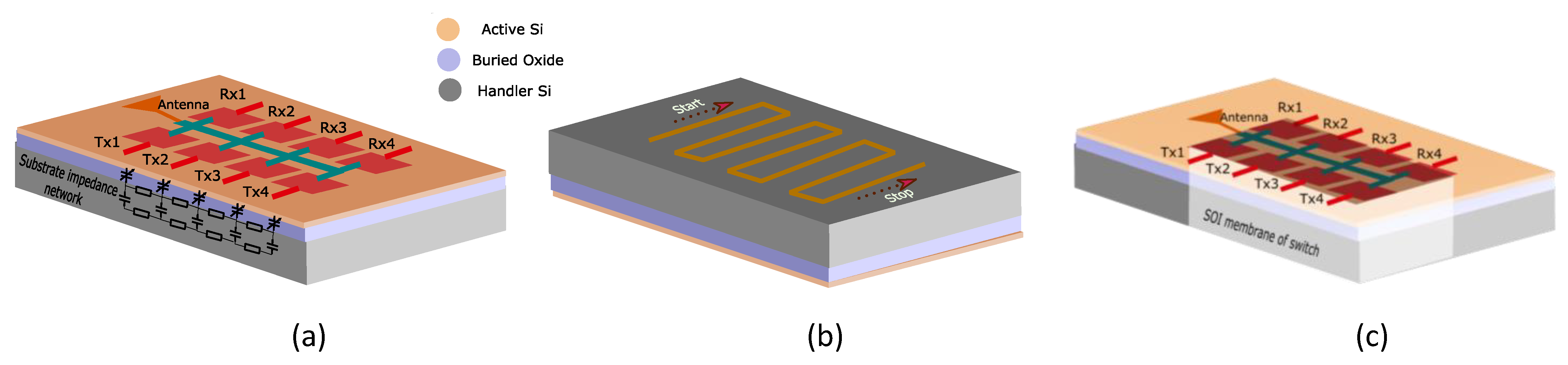
4. SP9T Switch Test Structure

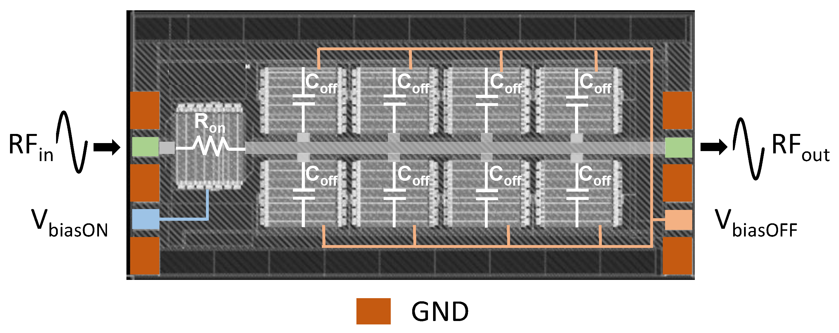
4.1. Device Structure, RF Ports and DC Bias

An SP9T switch test structure is utilized in this work for a demonstration of practical application. As in the case of capacitive combs, the switch is fabricated based on the 130 nm H9SOIFEM process technology by STMicroelectronics [28]. The switch features nine branches, each composed of a block comprising unitary n-type MOS transistors assembled in parallel to lower the on-state resistance and stacked in series to sustain high voltage. It constitutes a variation with respect to the series–shunt architecture as described in [32]. One branch biased in the ON state receives the input RF signal, which is propagated to the output along a line on which the eight other branches in the OFF state are connected as shown in Figure 8. As a result, this structure is a test vehicle. This means that it does not embody the full functionality of the SP9T switch, but tends to replicate its operation in a typical case where one serial branch is ON to propagate the signal from one port to the output while the other eight serial branches are OFF to block the inputs of the other eight ports. This structure has been designed to fully capture and better exacerbate the effects of loss and non-linearity related to the substrate on the useful signal propagated through the port in the ON state. The following parameters pertaining to the switch are measured: small-signal losses and linearity with respect to second and third harmonic (H2/H3) measurements. The OFF branches have a ground termination at the input. To control the ON/OFF state of the different branches, the switch features two DC bias pins. The ON/OFF terminals of the body and gate are controlled by these bias pins via a high series resistance for isolation between the RF signal and these control terminals [33]. The first pin is VbiasON, which puts one branch in the ON state by means of a positive bias voltage applied to both gate and body. Two bias voltages for the ON branch are used, namely, 2.5 V and 3.3 V, keeping in mind that a higher bias voltage gives a lower on-state resistance (Ron) for this branch.
The second pin is VbiasOFF, which puts the remaining eight branches in the OFF state by using a negative bias also applied simultaneously to both the gate and body. Here, VbiasOFF is set to −1.75 V. This negative bias enhances the cut-off state of the non-transmitting branches and results in a lower off-state capacitance (Coff). Two implementations of the switch are characterized with different gate lengths: 180 nm and 220 nm. The layout area of each implementation is 1.26 × 0.86 mm2.
From a post-processing point of view, microscopy characterizations ensure that the silicon underneath the BOX is completely removed, leading to a suspended membrane with only the useful functional layers. The cross-sectional image of the switch cavity after laser processing and prior to XeF2 etching is shown in Figure 9a.
This selective etching step is described in detail in [26,34]. After completion of XeF2 etching, the residual silicon handler is safely and cleanly removed as illustrated from DLM images shown in Figure 9b. It is worth noting that pictures are taken with the die flipped to ensure that no traces of silicon are left in the area of the switch after XeF2 etching.

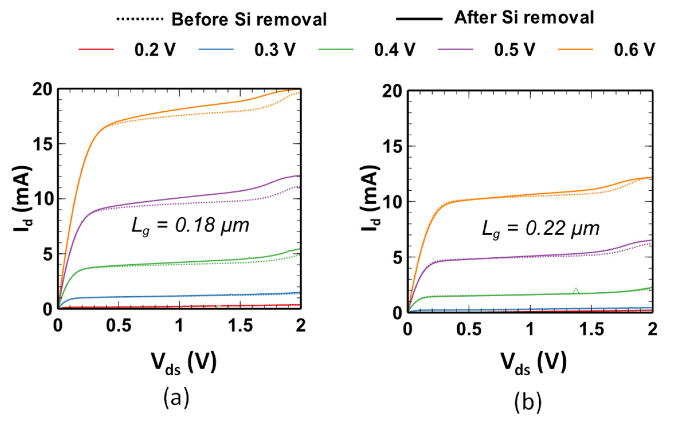
4.2. DC Characterization

DC characterization is carried out to provide an initial analysis of the switch performance after substrate removal. Additionally, the impact of the gate length on the switches ON-state characteristics is also highlighted. The gate bias for the ON branch (VbiasON) is varied and Ids−Vds characteristics are recorded. The results are plotted in Figure 10.
No significant difference in drain current (Ids) can be observed after silicon removal in the linear regime, indicating that any plausible variation in the strain level in the SOI film due to the membrane suspension does not induce an appreciable change in mobility. Instead, a slight increase in the saturation current is observed. Its amplitude is typically within the chip-to-chip dispersion range since measurements were not strictly performed on the same devices. Good agreement in Ids−Vds curves before and after substrate removal suggests that the physical integrity of the circuit stack is maintained despite the large size of the membrane. As expected, for the same applied gate voltage, the drain current is smaller for a 220 nm gate length as compared to its 180 nm counterpart. Hence, a smaller ON state resistance and insertion loss is anticipated for the 180 nm switch. Additionally, increasing the gate voltage reduces the resistance as observed by the slope of the Ids−Vds characteristics in the linear region which corresponds to its normal operation mode when used as an RF switch. The use of a smaller gate length and a higher gate drive is therefore favorable to a lower on-state resistance. This point is further corroborated when discussing S-parameter measurements in the following section.

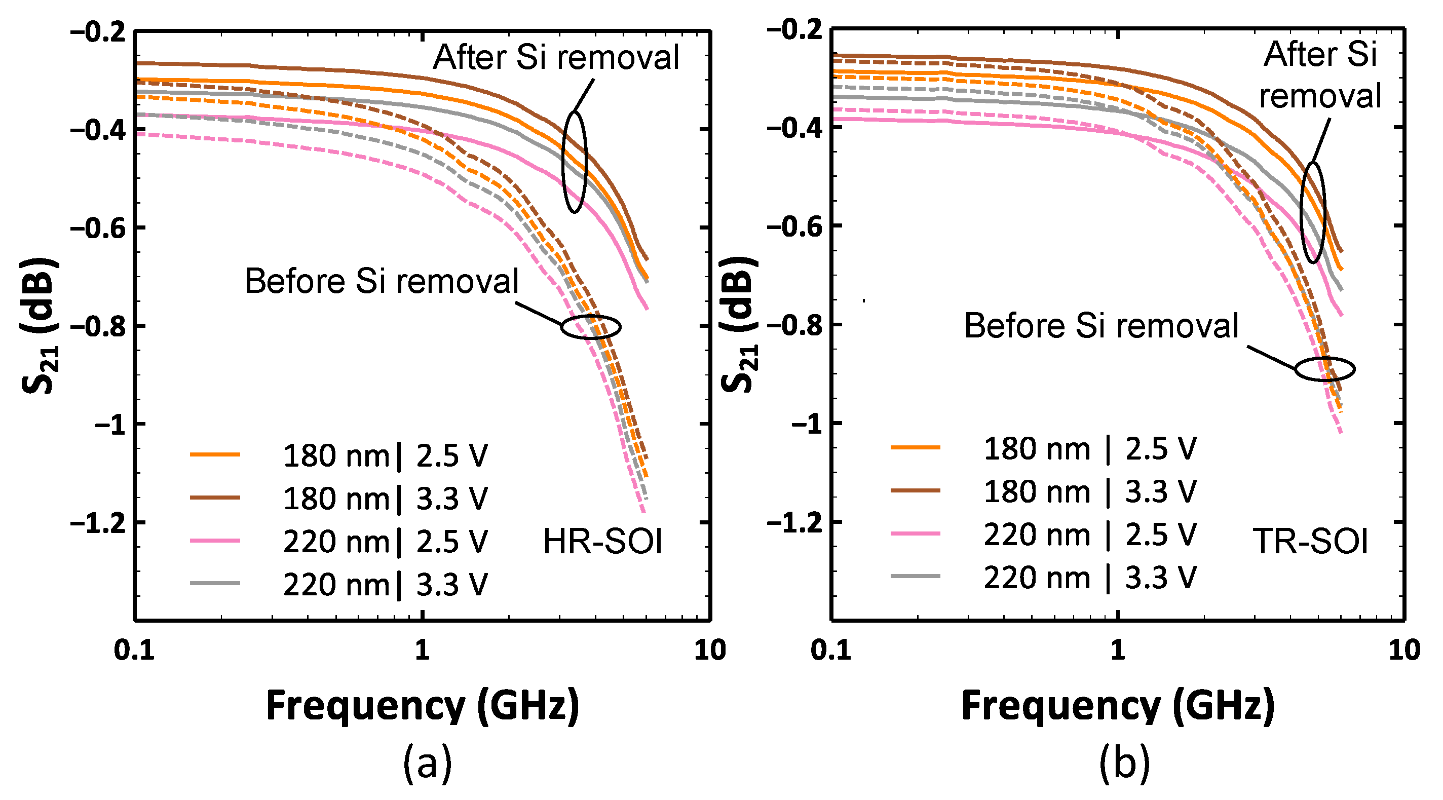
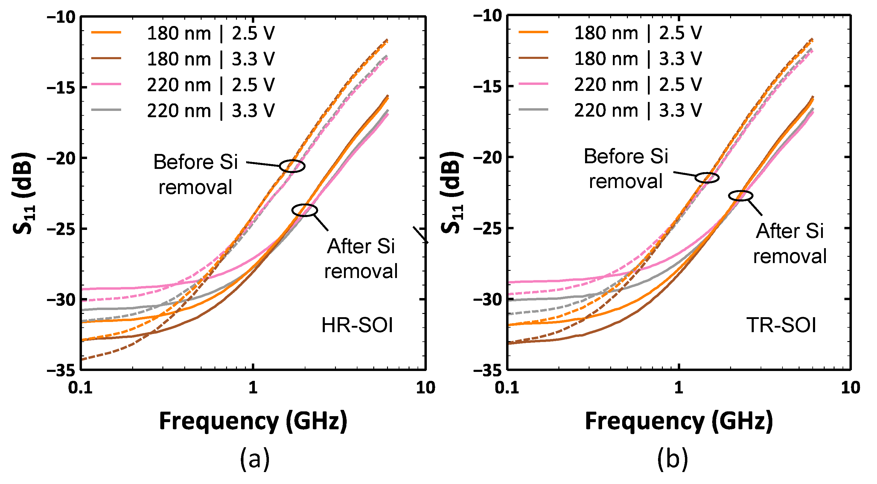
4.3. Two-Port S-Parameter Characterization

S-parameter measurements were performed on the SP9T switch test structure to determine the insertion loss and matching condition. The value of the insertion loss can be taken, approximately, as −S21 (dB) because the magnitude of the return signal on both ports is negligible compared to the transmitted one. The plots of the forward transmission coefficient S21 are shown in Figure 11. Before substrate removal, a gate drive of 3.3 V is favorable for smaller losses as compared to 2.5 V. Moreover, insertion losses are lesser for a gate length of 180 nm as compared to 220 nm. Both of these improvements can be attributed to the reduction in the on-state resistance of the transistor stack. Another observation is that insertion losses increase at a slightly faster rate as a function of frequency for the 180 nm switch. The difference in on-state resistance can also be clearly observed in the S11 graphs shown in Figure 12. At 100 MHz, Ron is the most dominant component as parasitic capacitances are negligible in this frequency range. A lower value of Ron entails less signal reflection at the switch input port and hence a lower value of S11. It can be clearly seen that S11 is lower for a smaller gate length and a higher gate voltage applied to the ON branch. As the frequency increases, the influence of OFF branches become more important in determining switch performance. It can be seen that at frequencies larger than 1 GHz, S11 curves overlap for both bias conditions. At 6 GHz, it is also observed that S11 is slightly lower for a gate length of 220 nm as compared to 180 nm. In the case of suspended membranes, the main insight derived from the S-parameter analysis is that the removal of the substrate helps to reduce insertion losses (IL). They remain about the same at MHz frequencies because Ron dominates them and subsequently decreases more noticeably at higher frequencies because Coff is reduced due to the absence of the silicon handler. It can also be noticed that the HR-SOI substrate features a higher insertion loss even at MHz frequencies. This can be appreciated by recalling the observations made in Figure 5 and Figure 6, which indicate that the substrate coupling is significantly greater at MHz frequencies for the HR-SOI substrate due to the depletion effect. At 6 GHz, the average improvement in S21 covering the four cases is 0.38 dB for HR-SOI and 0.26 dB for TR-SOI. These improvements can be directly attributed to the significant reduction in Coff in the OFF branches due to the elimination of substrate parasitics. This is also validated by observing a ~4 dB reduction in S11 for all four cases and both substrate types.
From a practical standpoint, it is worth noting that improvements such as those reported above can translate into a significant increase in the efficiency of the RF front end (ηTx), which can be calculated by considering the Tx path consisting of a power amplifier (PA) in series with the switch [35].
η T x = P o u t P i n
P o u t = η P A P i n P s w l o s s
where P i n is the input power to the PA, P s w l o s s is the power dissipated in the switch, P o u t is the power delivered to the antenna and η P A is the power amplifier efficiency. If we consider a PA with 50% efficiency delivering a power of 1 W (30 dBm) to the switch input, this implies that P i n is 2 W. The overall Tx efficiency in the 180 nm case with VbiasON of 3.3 V can be calculated at a frequency of 6 GHz as 39.5% and 40.4% for the HR-SOI and TR-SOI substrates, respectively, while it rises to 43% after membrane suspension for both substrate types. This corresponds to an efficiency improvement of 3.5% and 2.6%, respectively, when comparing the suspended membranes to their HR-SOI and TR-SOI counterparts without backside micromachining. While the actual improvement in efficiency depends on the front end architecture, this calculation shows the importance of losses in the switch building block.

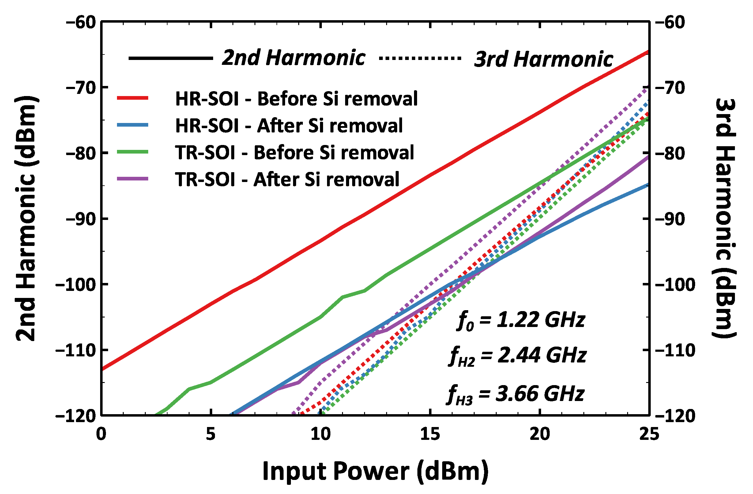
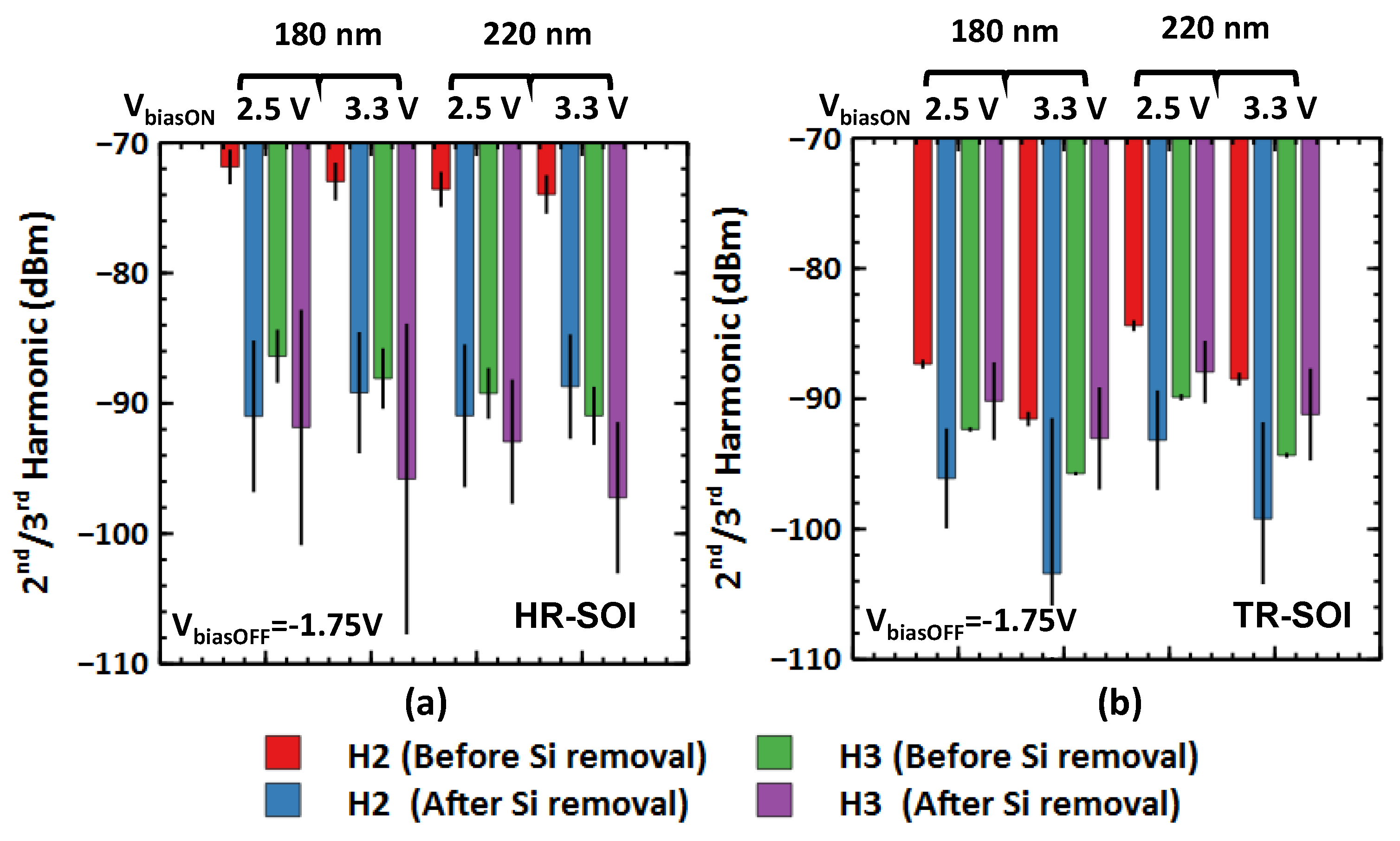
4.4. Large-Signal Harmonic Distortion

Harmonic distortion measurements were performed to characterize the effect of substrate removal on linearity. The measurement is performed at a fundamental input frequency of 1.22 GHz, while the second and third harmonics (H2/H3) are measured at the output at frequencies of 2.44 and 3.66 GHz, respectively. A low noise floor setup as described in [34] is used for the measurement. The input power is swept at the fundamental frequency and the second and third harmonic power is recorded as shown in Figure 13. The number of processed samples for harmonics’ characterization is four and five for the HR-SOI and TR-SOI substrates, respectively. As shown in Figure 14, the dispersion of measured data is low before substrate removal and can therefore be expected to be the same for the characterization after membrane suspension. However, the scatter after substrate removal proves to be higher. This can be attributed to cumulative effects such as processing defects, poor probe contact due to pad degradation after probing multiple times, non-linearities introduced by the degraded pad and offset between the targeted area and the actual area of silicon removal.
Despite this difficulty, Figure 14 shows very clearly a distinctive downward trend in harmonics with a reduction level well beyond the dispersion range. In a switch, the second order non-linearities are dominated by Coff, and third order non-linearities depend on both Ron and Coff [16,36]. With an increase in the gate voltage of the ON branch, both second and third harmonics levels reduce [37]. This trend is observed on switches with both 180 nm and 220 nm gate lengths and for both substrates before and after membrane suspension. There is an overall improvement in H2 for both types of substrate regardless of the gate length and bias conditions after silicon removal. A detailed study of H2 for different substrate types has been performed in [38]. For transistor stack in the OFF state, it has been shown that at a body bias of <−1.5 V, the substrate parasitics start to dominate over the device parasitics. It was also observed in the case of the coupling test structures in Section 3 that the HR-SOI substrate has a much more pronounced non-linear behavior compared to its TR-SOI counterpart. Before substrate removal, the H2 level is therefore significantly higher for the HR-SOI substrate. As membrane suspension leads to the total elimination of the substrate parasitics, less harmonic distortion is expected. Accordingly, a remarkable average reduction in H2 is established at 17.7 dB and 16.1 dB for switches initially processed on an HR substrate with gate lengths of 180 nm and 220 nm, respectively. More interestingly, measurements show that after membrane suspension, H2 is also substantially reduced by 10.3 dB and 9.8 dB at 180 nm and 220 nm gate lengths, respectively, for the switches originally fabricated on TR substrate. This last observation might seem to contradict the study of capacitive coupling structures in Section 3, which concluded that the potential pinning effect introduced by the buried polysilicon layer of the TR substrate was shielding the non-linear effects coming from the handler. Although this effect is particularly effective in screening effects related to parasitic depletion or parasitic interface conduction in the silicon handler, the 10 dB reduction in H2 after membrane suspension demonstrates that it is still possible to progress beyond the use of a TR substrate, which echoes the objective stated in the introduction of exploring the ultimate performance margins. For the third harmonic, an average reduction of 7.8 dB is obtained in the case of the HR-SOI substrate. On the other hand, the margin of dispersion of H3 measurements does not allow any difference between the suspended switch and its reference on handler to be appreciated.

5. Conclusions

A novel fabrication method using laser processing is presented, which paves the way for local handler substrate removal of SOI RF circuits. Membranes of capacitive comb structures were first studied to delineate the importance of substrate in the performance of an RF circuit. Based on handler removal, it was shown that coupling is significantly reduced and any starting substrate can be used to arrive at the same final performance. An SP9T test structure was described and characterized to demonstrate the practical utility of laser processing in a real application scenario. The impact of eliminating the silicon handler locally on the reduction in the capacitive coupling of the OFF transistor branches was highlighted. Substantial gains in improvements were obtained. A reduction in the insertion loss by 0.38 dB and 0.26 dB was obtained for HR-SOI and TR-SOI substrates, respectively. Calculations of front end efficiency revealed that ~3% improvement can be reached by substrate removal. In addition to the amelioration of losses, large signal linearity was also greatly enhanced. The second harmonic was suppressed further by up to 17.7 dB and 10.3 dB for HR-SOI and TR-SOI substrates, respectively. These results demonstrate the significance of local substrate removal methods to greatly improve the RF performance of the circuit and open up new avenues for RF designers to evaluate ultimate circuit performance in the absence of substrate-induced dissipative losses and non-linear effects.

Author Contributions

Conceptualization, methodology, software, validation, formal analysis, investigation, writing—original draft, review and editing, visualization, A.B.; resources, validation, J.P., E.O., F.B. and J.-F.R.; conceptualization, investigation, C.D. and F.G.; investigation, supervision, writing—review and editing, project administration, funding acquisition, D.G.; supervision, project administration, C.G.; conceptualization, methodology, validation, formal analysis, investigation, writing—original draft, review and editing, supervision, project administration, funding acquisition, E.D. All authors have read and agreed to the published version of the manuscript.

Funding

This research was funded by: (i) the STMicroelectronics-IEMN joint laboratory, (ii) the French government through the National Research Agency (ANR) under program PIA EQUIPEX LEAF ANR-11-EQPX-0025 and (iii) the French RENATECH network on micro and nanotechnologies.

Institutional Review Board Statement

Not applicable.

Informed Consent Statement

Not applicable.

Data Availability Statement

Not applicable.

Acknowledgments

The author would like to thank Jerome Lajoinie and Philippe Cathelin from STMicroelectronics for structure design and RF switch concept discussions.

Conflicts of Interest

The authors declare no conflict of interest.

References

  1. Solutions, I.S. Choosing the Right RF Switches for Smart Mobile Device Applications; Technical Report; Skyworks Solutions, Inc.: Irvine, CA, USA, 2011. [Google Scholar]
  2. Li, J.Y.; Chang, W.-C. Wideband and high isolation RF carrier-aggregated switch module for LTE-Advanced base station. In Proceedings of the European Microwave Conference (EuMC), London, UK, 4–6 October 2016; pp. 695–698. [Google Scholar]
  3. Chiu, H.C.; Yeh, T.J.; Hsieh, Y.Y.; Hwang, T.; Yeh, P.; Wu, C.S. Low insertion loss switch technology using 6-inch InGaP/AlGaAs/InGaAs pHEMT production process. In Proceedings of the IEEE Compound Semiconductor Integrated Circuit Symposium, Monterey, CA, USA, 24–27 October 2004; pp. 119–122. [Google Scholar]
  4. Kelly, D.; Brindle, C.; Kemerling, C.; Stuber, M. The state-of-the-art of silicon-on-sapphire CMOS RF switches. In Proceedings of the IEEE Compound Semiconductor Integrated Circuit Symposium, Palm Springs, CA, USA, 30 October–2 November 2005; p. 4. [Google Scholar]
  5. Blaschke, V.; Unikovski, A.; Hurwitz, P.; Chaudhry, S. A SP9T cellular antenna switch in 2.5 V CMOS thin-film SOI. In Proceedings of the IEEE Topical Meeting on Silicon Monolithic Integrated Circuits in RF Systems, Austin, TX, USA, 21–23 January 2013; pp. 144–146. [Google Scholar]
  6. Im, D.; Lee, K. Characterization and optimization of partially depleted SOI MOSFETs for high power RF switch applications. J. Solid-State Electron. 2013, 90, 94–98. [Google Scholar] [CrossRef]
  7. Tinella, C.; Fournier, J.M.; Belot, D.; Knopik, V. A 0.7 dB insertion loss CMOS-SOI antenna switch with more than 50 dB isolation over the 2.5 to 5GHz band. In Proceedings of the European Solid-State Circuits Conference, Florence, Italy, 24–26 September 2002; pp. 483–486. [Google Scholar]
  8. Kim, D.; Min, B.W. High Power Ku-Band T/R and SP4T Switches in SOI CMOS. J. Electromagn. Waves Appl. 2016, 30, 728–739. [Google Scholar] [CrossRef]
  9. Rack, M.; Allibert, F.; Raskin, J.-P. Modeling of Semiconductor Substrates for RF Applications: Part I—Static and Dynamic Physics of Carriers and Traps. IEEE Trans. Electron Devices 2021, 68, 4598–4605. [Google Scholar] [CrossRef]
  10. Rack, M.; Allibert, F.; Raskin, J.-P. Modeling of Semiconductor Substrates for RF Applications: Part II—Parameter Impact on Harmonic Distortion. IEEE Trans. Electron Devices 2021, 68, 4606–4613. [Google Scholar] [CrossRef]
  11. Ali, K.B.; Neve, C.R.; Gharsallah, A.; Raskin, J.P. RF Performance of SOI CMOS Technology on Commercial 200-mm Enhanced Signal Integrity High Resistivity SOI Substrate. IEEE Trans. Electron Devices 2014, 61, 722–728. [Google Scholar] [CrossRef]
  12. Kerr, D.C.; Gering, J.M.; McKay, T.G.; Carroll, M.S.; Neve, C.R.; Raskin, J.P. Identification of RF harmonic distortion on Si substrates and its reduction using a trap-rich layer. In Proceedings of the IEEE Topical Meeting on Silicon Monolithic Integrated Circuits in RF Systems, Orlando, FL, USA, 23–25 January 2008; pp. 151–154. [Google Scholar]
  13. Liu, S.; Zhu, L.; Allibert, F.; Radu, I.; Zhu, X.; Lu, Y. Physical Models of Planar Spiral Inductor Integrated on the High-Resistivity and Trap-Rich Silicon-on-Insulator Substrates. IEEE Trans. Electron Devices 2007, 64, 2775–2781. [Google Scholar] [CrossRef]
  14. Mueller, J.E.; Bruder, T.; Herrero, P.; Norholm, N.; Olesen, P.; Rizk, J.; Schumacher, L. Requirements for reconfigurable 4G front-ends. In Proceedings of the IEEE MTT-S International Microwave Symposium Digest, Seattle, WA, USA, 2–7 June 2013; pp. 1–4. [Google Scholar]
  15. Tombak, A.; Iversen, C.; Pierres, J.B.; Kerr, D.; Carroll, M.; Mason, P.; Spears, E.; Gillenwater, T. Cellular antenna switches for multimode applications based on a Silicon-on-Insulator technology. In Proceedings of the IEEE Radio Frequency Integrated Circuits Symposium, Anaheim, CA, USA, 23–25 May 2010; pp. 271–274. [Google Scholar]
  16. Shaked, Z.; Hurwitz, P.; Heiman, A.; Moen, K.; Kanawati, R.; Chaudhry, S.; Racanelli, M. SOI technology for front end applications. In Proceedings of the IEEE International Conference on Microwaves, Communications, Antennas and Electronic Systems (COMCAS), Tel Aviv, Israel, 2–4 November 2015; pp. 1–3. [Google Scholar]
  17. Tagro, Y.; Lecavelier des Etangs-Levallois, A.; Poulain, L.; Lepilliet, S.; Gloria, D.; Raynaud, C.; Dubois, E.; Danneville, F. High frequency noise potentialities of reported CMOS 65 nm SOI technology on flexible substrate. In Proceedings of the IEEE Topical Meeting on Silicon Monolithic Integrated Circuits in RF Systems, Santa Clara, CA, USA, 16–18 January 2012; pp. 89–92. [Google Scholar]
  18. Lecavelier des Etangs-Levallois, A.; Lesecq, M.; Danneville, F.; Tagro, Y.; Lepilliet, S.; Hoel, V.; Troadec, D.; Gloria, D.; Raynaud, C.; Dubois, E. Radio-frequency and low noise characteristics of SOI technology on plastic for flexible electronics. Solid-State Electron. 2013, 90, 73–78. [Google Scholar] [CrossRef]
  19. Philippe, J.; Lecavelier des Etangs-Levallois, A.; Berthome, M.; Robillard, J.F.; Gaquiere, C.; Danneville, F.; Gloria, D.; Raynaud, C.; Dubois, E. Application-oriented performance of RF CMOS technologies on flexible substrates. In Proceedings of the IEEE International Electron Devices Meeting (IEDM), Washington, DC, USA, 7–9 December 2015; pp. 15.7.1–15.7.4. [Google Scholar]
  20. Philippe, J.; Bhaskar, A.; Okada, E.; Braud, F.; Robillard, J.F.; Danneville, F.; Raynaud, C.; Gloria, D.; Dubois, D. Thermal Analysis of Ultimately-Thinned-and-Transfer-Bonded CMOS on Mechanically Flexible Foils. IEEE J. Electron Devices Soc. 2019, 7, 973–978. [Google Scholar] [CrossRef]
  21. Lecavelier des Etangs-Levallois, A.; Chen, Z.; Lesecq, M.; Lepilliet, S.; Tagro, Y.; Danneville, F.; Robillard, J.F.; Hoel, V.; Troadec, D.; Gloria, D.; et al. A converging route towards very high frequency, mechanically flexible, and performance stable integrated electronics. J. Appl. Phys. 2013, 113, 153701. [Google Scholar] [CrossRef]
  22. Lecavelier des Etangs-Levallois, A.; Dubois, E.; Lesecq, M.; Danneville, F.; Poulain, L.; Tagro, Y.; Lepilliet, S.; Gloria, D.; Raynaud, C.; Troadec, D. 150-GHz RF SOI-CMOS technology in ultrathin regime on organic substrate. IEEE Electron Device Lett. 2011, 32, 1510–1512. [Google Scholar] [CrossRef]
  23. Cheng, J.; Liu, C.S.; Shang, S.; Liu, D.; Perrie, W.; Dearden, G.; Watkins, K. A review of ultrafast laser materials micromachining. J. Opt. Laser Technol. 2013, 46, 88–102. [Google Scholar] [CrossRef]
  24. Leyder, S.; Grojo, D.; Delaporte, P.; Marine, W.; Sentis, M.; Utéza, O. Non-linear absorption of focused femtosecond laser pulses at 1.3 μm inside silicon: Independence on doping concentration. J. Appl. Surface Sci. 2013, 278, 13–18. [Google Scholar] [CrossRef]
  25. Ghosh, A. The 5G mmWave Radio Revolution. Microw. J. 2016, 59, 22–36. [Google Scholar]
  26. Bhaskar, A.; Philippe, J.; Braud, F.; Okada, E.; Avramovic, V.; Robillard, J.F.; Durand, C.; Gloria, D.; Gaquiere, C.; Dubois, E. Large-area femtosecond laser milling of silicon employing trench analysis, paper submitted. J. Opt. Laser Technol. 2021, 138, 106866. [Google Scholar] [CrossRef]
  27. Bhaskar, A. Substrate Engineering Using Laser Micromachining for Improvement of RF Devices and Systems Integrated in SOI-CMOS Technology. Ph.D. Thesis, University of Lille, Lille, France, 2019. [Google Scholar]
  28. Gianesello, F.; Monroy, A.; Vialla, V.; Canderle, E.; Bertrand, G.; Buczko, M.; Coly, M.; Nowakowski, J.; Revil, N.; Rolland, L.; et al. Highly linear and sub 120 fs Ron × Coff 130 nm RF SOI technology targeting 5G carrier aggregation RF switches and FEM SOC. In Proceedings of the Topical Meeting on Silicon Monolithic Integrated Circuits in RF Systems, Austin, TX, USA, 24–27 January 2016; pp. 9–12. [Google Scholar]
  29. Bhaskar, A.; Philippe, J.; Avramovic, V.; Braud, F.; Robillard, J.F.; Durand, C.; Gloria, D.; Gaquiere, C.; Dubois, E. Substrate engineering of inductors on SOI for improvement of Q-factor and application in LNA. IEEE J. Electron Devices Soc. 2020, 8, 959–969. [Google Scholar] [CrossRef]
  30. Dubois, E.; Larrieu, G.; Valentin, R.; Breil, N.; Danneville, F. Introduction to Schottky-Barrier MOS Architectures: Concept, Challenges, Material Engineering and Device Integration. In Nanoscale CMOS: Innovative Materials, Modeling and Characterization; Balestra, F., Ed.; ISTE Ltd.: London, UK, 2010; Chapter 5; pp. 157–204. [Google Scholar]
  31. Tung, R.T. Recent advances in Schottky barrier concepts. Mater. Sci. Eng. 2001, R35, 1–138. [Google Scholar] [CrossRef]
  32. Li, X.; Zhang, Y. Flipping the CMOS Switch. IEEE Microw. Mag. 2010, 11, 86–96. [Google Scholar] [CrossRef]
  33. Zhang, Z.; Zhang, G.; Yu, K.; Lin, J.; Huang, L. Effects and contrasts of silicon-on-insulator floating-body and body-contacted field-effect transistors to the design of high-performance antenna switches. IET Microw. Antennas Propag. 2016, 10, 507–516. [Google Scholar] [CrossRef]
  34. Bhaskar, A.; Philippe, J.; Berthome, M.; Okada, E.; Robillard, J.F.; Gloria, D.; Gaquière, C.; Dubois, E. Large-area femtosecond laser ablation of Silicon to create membrane with high performance CMOS-SOI RF functions. In Proceedings of the IEEE Electronic System-Integration Technology Conference (ESTC), Dresden, Germany, 18–21 September 2018; pp. 1–6. [Google Scholar]
  35. Choi, P.; Goswami, S.; Radhakrishna, U.; Khanna, D.; Boon, C.C.; Lee, H.S.; Antoniadis, D.; Peh, L.S. A 5.9-GHz Fully Integrated GaN Frontend Design With Physics-Based RF Compact Model. IEEE Trans. Microw. Theory Tech. 2015, 63, 1163–1173. [Google Scholar] [CrossRef]
  36. Yu, B.; Ma, K.; Meng, F.; Yeo, K.S.; Shyam, P.; Zhang, S.; Verma, P.R. DC-30 GHz DPDT switch matrix design in high resistivity trap-rich SOI. IEEE Trans. Electron Devices 2017, 64, 3548–3554. [Google Scholar] [CrossRef]
  37. Yu, B.; Ma, K.; Meng, F.; Yeo, K.S.; Shyam, P.; Zhang, S.; Verma, P.R. Ultra-Wideband Low-Loss Switch Design in High-Resistivity Trap-Rich SOI With Enhanced Channel Mobility. IEEE Trans. Microw. Theory Tech. 2017, 65, 3937–3949. [Google Scholar] [CrossRef]
  38. Kazemi Esfeh, B.; Rack, M.; Makovejev, S.; Allibert, F.; Raskin, J.P. A SPDT RF Switch Small- and Large-Signal Characteristics on TR-HR SOI Substrates. IEEE J. Electron Devices Soc. 2018, 6, 543–550. [Google Scholar] [CrossRef]
Figure 1. (a) Illustration showing the presence of substrate parasitics in RF switch; (b) trajectory of laser beam in the milling process to locally remove silicon from the back side; (c) SOI membrane of switch showing complete local removal of handler silicon and, consequently, substrate parasitics.
Electronics 11 02333 g001
Figure 2. (a) Three-dimensional view of capacitive coupling structures showing interdigitated fingers; (b) top view; (c) cross-sectional view.
Electronics 11 02333 g002
Figure 3. DLM images of capacitive coupling structures suspended in a membrane after substrate removal: (a) CPL-A/HR-SOI; (b) CPL-A/TR-SOI; (c) CPL-B/HR-SOI; (d) CPL-B/TR-SOI.
Electronics 11 02333 g003
Figure 4. Extraction of capacitive coupling between interdigitated electrode combs. (a) Principle of extraction of coupling admittance YC from the measured admittance matrix Yij; (b) extraction of coupling capacitance CTOT; (c) extraction of capacitance CTOP after local substrate removal; (d) deduction of the substrate coupling capacitance.
Electronics 11 02333 g004
Figure 5. Coupling capacitance between the electrode combs. CTOTAL is the total measured capacitance, CTOP is the capacitance mainly associated with the interconnects, CSUB represents the contribution of the substrate to the lateral capacitive coupling. (a) Structure CPL-A; (b) structure CPL-B.
Electronics 11 02333 g005
Figure 6. Coupling capacitances between the electrode combs of structure CPL-B at chuck bias of −2.5, 0 and 2.5 V. CTOTAL is the total measured capacitance, CTOP is the capacitance mainly associated with the interconnects, CSUB represents the contribution of the substrate to the lateral capacitive coupling. (a) HR starting substrate; (b) TR starting substrate.
Electronics 11 02333 g006
Figure 7. Forward loss factor of structure CPL-A at chuck bias of −2.5, 0 and 2.5 V. FLFTOTAL and FLFTOP are the loss factors before and after substrate removal, respectively. (a) HR starting substrate; (b) TR starting substrate.
Electronics 11 02333 g007
Figure 8. Layout of SP9T switch test structure showing the individual contact terminals in the GSGSG configuration for probing with the ON or OFF state of each branch represented by Ron or Coff, respectively.
Electronics 11 02333 g008
Figure 9. (a) SEM cross-sectional image of cavity fabricated using laser processing. The hatched zone corresponds to residual silicon left after laser processing and before XeF2 selective etching; (b) 3D rendered backlight illuminated optical microscope image.
Electronics 11 02333 g009
Figure 10. Static Ids−Vds characteristics of the ON branch of the SP9T switch structure on TR-SOI substrate before and after silicon removal based on unitary MOS transistors with two different gate lengths (a) 180 nm; (b) 220 nm.
Electronics 11 02333 g010
Figure 11. S21 curves depicting the transmission characteristics of the switch before and after substrate removal for different gate lengths and VbiasON values (a) HR-SOI; (b) TR-SOI.
Electronics 11 02333 g011
Figure 12. S11 curves depicting the reflection losses of the switch before and after substrate removal for different gate lengths and VbiasON values (a) HR-SOI; (b) TR-SOI.
Electronics 11 02333 g012
Figure 13. Harmonic distortion shown for a sample with gate length of 220 nm and VbiasON = 2.5 V.
Electronics 11 02333 g013
Figure 14. Second/third harmonic levels for different gate lengths (180 or 220 nm) and bias conditions (VbiasON = 2.5 or 3.3 V, VbiasOFF = −1.75 V) before and after substrate removal: (a) HR-SOI substrate; (b) TR-SOI substrate.
Electronics 11 02333 g014
Table 1. Dimensions of the studied capacitive coupling structures.
ReferenceNo. of Fingersdif
(µm)
W
(µm)
Wfinger
(µm)
CPL-A618.3269.710.7
CPL-B811.3269.710.7
Table 2. ΔS21 values depicting the difference in substrate coupling before and after removal of substrate at chuck bias of 0 V.
ReferenceΔS21 (dB) (HR-SOI)ΔS21 (dB) (TR-SOI)
20 MHz5 GHz20 MHz5 GHz
CPL-A156.810.77.5
CPL-B135.28.95.2
Publisher’s Note: MDPI stays neutral with regard to jurisdictional claims in published maps and institutional affiliations.

