1. Introduction
The design process of most analog building blocks is a manual and time-consuming process that requires a high level of expertise. In addition, the effort required for the design process needs to be repeated every time the technology or the circuit specifications are changed. On the other hand, digital circuit design is automated using industry-standard tools that enable the designer to synthesize most of the digital building blocks in a fast and efficient procedure. This disparity in design time and effort between the analog and digital blocks has directed researchers toward trying to automate the analog design process [
1,
2].
The analog design process can be divided into a series of iterative steps that starts with topology selection followed by transistor sizing, layout, verification, and finally, post-layout verification. The task of topology selection usually depends on the designer’s experience and intuition. The designer must decide which topology is most suitable to achieve the required specifications [
3]. The level of expertise required for correct topology selection may not be available. In addition, with the increased number of topologies performing the same functionality, it is becoming harder for the designer to solely rely on his experience to choose the topology that will better achieve the required specifications. Moreover, the decision may be sub-optimal, i.e., the chosen topology may achieve the specifications but with extra power and area.
As a result, topology selection automation is proving to be an important task. One strategy that has been investigated in automating the topology selection process is an equation-based selection [
4]. In this method, the design parameters are related to the design specifications through a set of linearized relations. After that, the design parameters are swept to cover the whole design space, and the range of achievable output specifications is determined. This method suffers greatly from inaccuracy due to the simplified equations used.
Another approach that has been investigated to automate the topology selection process is the development of a choosing algorithm that depends on a set of rules to choose the suitable topology for the required specifications [
5]. This set of rules is determined by an expert designer. The drawback of such a method is that it is not an accurate method, as it relies on a designer’s experience. Another drawback is that it does not produce an optimal selection for the topology. Moreover, the rules may fail when the technology or the device type change.
With recent advancements in computer processing capabilities, machine learning and neural networks have emerged as exciting candidates for the automation of analog design and have been used in the automation of the synthesis and design of analog circuits with fixed topologies to achieve a set of specifications [
1,
6].
In this paper, we present an approach for the usage of neural networks for the selection of a suitable analog amplifier topology for a set of specifications. The required specifications serve as input parameters for the network while the circuit topology is the output of the classification problem. The network is trained on the fly to allow changing the set of specifications used for topology selection. A modified cascaded neural network that involves performing the prediction on two stages is then presented. The performance of the two approaches is compared showing that the cascaded network has better performance and gives the designer an agile approach for topology selection.
2. Data Generation
The topologies chosen for the neural network training are all topologies that perform the same functionality, namely, CMOS integrated analog amplifier topologies with a differential input and a single-ended output. In our study, 30 different topologies are chosen. The topologies chosen included many varieties that are demonstrated in
Table 1. A supply voltage of 1.8 V and a 180 nm CMOS technology was used for all topologies.
The dataset was generated using the Analog designer’s toolbox (ADT) [
7], which is an analog design automation tool that uses lookup tables (LUTs) extracted from the simulator to predict the behavior of a circuit in a fast and efficient way [
8]. For each topology, the design parameters were swept in the entire design space, and the corresponding specifications were obtained. The bias point of every device was swept in the gm/ID space to ensure that the generated circuits are correct-by-construction, i.e., all the transistors are properly biased in saturation [
9]. Any circuit that has invalid biasing conditions is automatically discarded from the dataset. The total number of dataset training points obtained for all circuits was ≈480,000 circuits. The time taken to generate those training examples was 1.2 min. In addition to being generated in a very short time, this is a one-time effort that needs to be done only once.
The specifications measured in the dataset generation are presented in
Table 2 along with the minimum and maximum obtained values for each specification. Since the degrees of freedom of the devices in every design were extensively searched in the generation process, each specification has a very wide range of values, e.g., Open-loop DC Voltage Gain from 13 to 1.9 M. Since the amplifier circuits included in the study may have several poles, a significant phase shift may be introduced, leading to a negative phase margin (PM). On the other hand, the amplifier may have a single pole that is not far away from the unity-gain frequency; thus, the phase shift is small, leading to a quite large PM. Some of the generated designs may have outlier specifications with low practical value; e.g., a negative or low PM will make the circuit unstable if the loop is closed. However, there is no prior assumptions about how the amplifier circuit is going to be used, e.g., open loop or closed loop, type of feedback network, etc. Since the PM is calculated assuming a unity-feedback factor, the actual PM may be acceptable depending on the feedback network used by the designer. Moreover, this will not affect the topology selection process because the specifications entered by the designer will target circuits of practical value. If a specific range of specs is required for the given design problem, e.g., PM is required to be between 30° and 90°, the invalid design points can be removed from the dataset before the training process.
To be able to test the neural network’s algorithms constructed in this paper, a subset of the generated dataset is separated for testing. This subset consists of 1200 design points selected by randomly choosing 40 examples from each topology. The testing examples are removed from the pool of the available circuits for training.
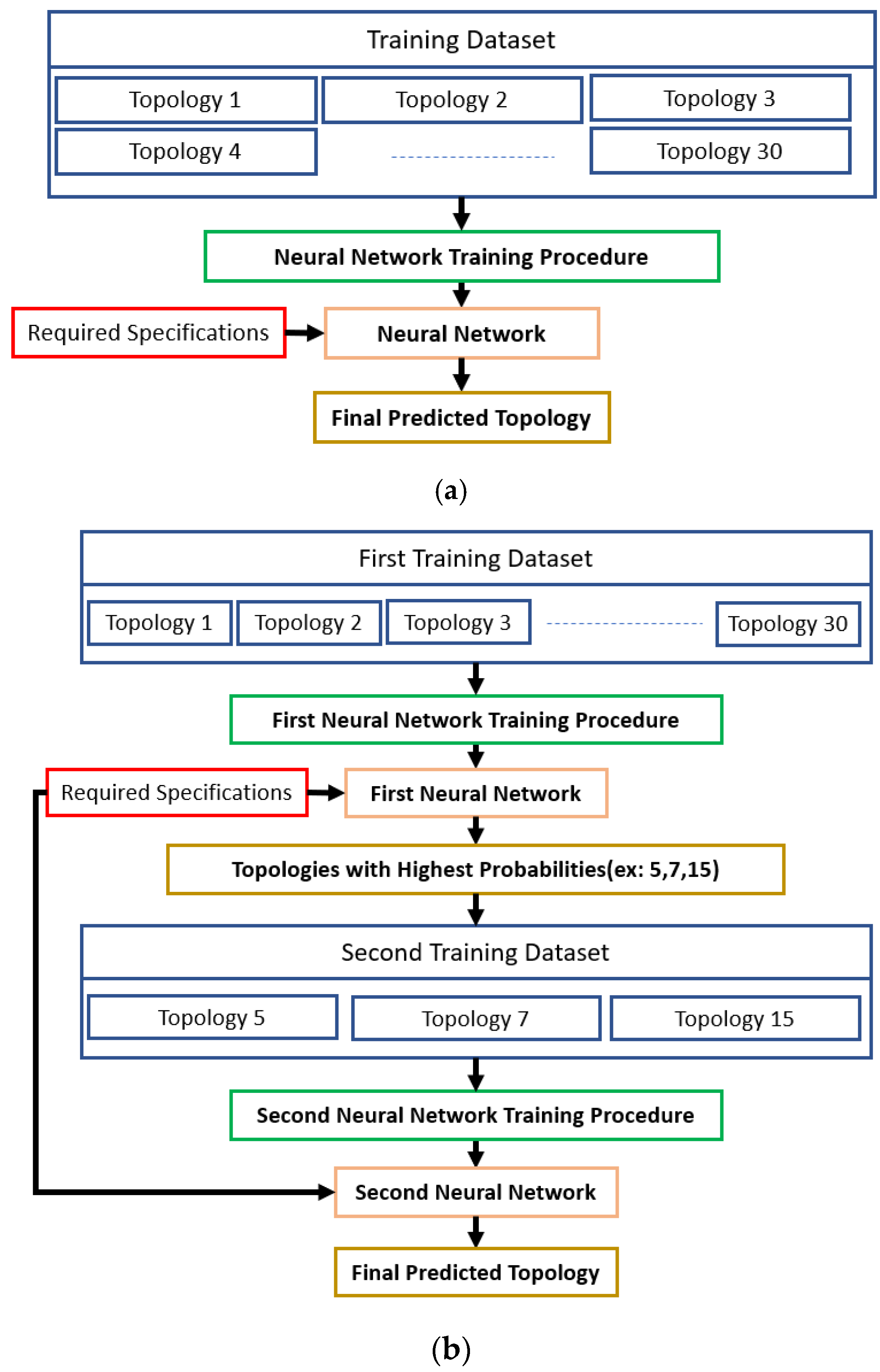
3. The First Approach
In the first approach, a single neural network is constructed and trained with the training examples such that the input to the network is the required specifications and the output is the suitable topology to achieve those specifications as depicted in
Figure 1a. The neural network was constructed using TensorFlow [
10] and Python. It is formed of two hidden layers each of which consists of 200 nodes with the activations function of ReLU. The output activation function is the sigmoid function. The learning rate was fixed at
, and Adam optimizer was used with a loss function of mean square error. The number of epochs was fixed to 200 epochs. The network was trained using 480,000 training examples. It was then tested using the testing set that consists of 1200 examples. The network succeeded in predicting the correct topology in 1145 examples of the 1200 testing examples. The achieved R
2 score is 0.9.
The training time of this network is two hours. This training time can be tolerated if this training is a one-time effort completed at the beginning. However, this puts a restriction on the specifications used in prediction because the whole set of specifications needs to be determined to obtain an accurate prediction. Most of the time, the designer wants to decide on a topology to achieve only a subset of the mentioned specifications in
Table 2. To solve this problem, the training needs to be completed on the fly before every prediction. This puts a tight requirement on the training time. In order to reduce training time, the training dataset size can be reduced. However, this will be at the expense of the accuracy.
4. The Second Approach
To reduce the training time and maintain a good prediction accuracy, another approach is proposed. The prediction is performed on two stages (coarse and fine). In the first stage (the coarse stage), a neural network is trained to predict the suitable topology based on a smaller amount of training examples. The results of this prediction step are not as good as the results obtained when a huge number of training examples is used as in the first approach. To improve this coarse prediction, the classes with the highest probability of matching the required specifications based on this network are used as an input for a second stage that is used to improve the prediction (the fine stage).
In the second stage (the fine network), the second neural network is trained using only data examples from topologies that produced a high probability of achieving the required specifications as predicted by the first network. Only circuit topologies that achieved a probability of more than 10% for achieving the required specifications in the first network were used as possible contenders in the second network. This means that a smaller number of topologies is used in the dataset of the second network. This allows for more training examples for each topology while maintaining the total number of examples below a certain limit to keep the training time of the second network also small. The methodology used in this second approach is summarized in
Figure 1b.
To implement this approach, the first step was to determine the size of the training set of the first network to have a good accuracy such that correct topologies would be selected as contenders to choose from for the second network. The size of the training set was reduced multiple times, and the accuracy of the test set was compared to the accuracy of the first approach. The number of testing examples that had the correct topology included in the list of contenders for the second network was also compared (inclusion in the top contenders). If the correct topology is included as a contender for the second network, there is a chance the second network can choose it as the correct topology to achieve the specifications after fine training. The training time was also recorded. The results of such a comparison are shown in
Table 3. It is clear from
Table 3 that the training time decreases exponentially as the training set size is decreased.
For the second stage (the fine network), a dataset consisting of topologies that scored a probability of higher than 10% in the first network is used. For each topology, the number of training examples used is increased by a factor of 33× compared to the first network to improve the prediction. The fine network consists of two hidden layers, each of which consists of 200 neurons with the activation function ReLU. The output layer was also using a sigmoid activation function. The learning rate was fixed at , and Adam optimizer was used with a loss function of mean square error. Only 100 epochs were used in this network, unlike 200 in the first network, to reduce the training time. This network is trained for each input separately based on the results of the previous network. The network was tested for each of the 1200 examples of the testing set. If the list of possible contender topologies resulting from the first network for a certain set of specifications includes only one topology, this topology is taken as the final prediction without the need for the second stage of training.
5. Results
The results of the single neural network using two sizes of datasets are compared to the results of the second approach (the two-stage approach) in terms of accuracy and training time in
Table 4. A standard Core i7 9th generation 2.6 GHz processor was used in all the experiments. The single network achieves 95.4% accuracy in two hours using 480,000 training examples and 90.6% accuracy in 3.6 min using 48,000 examples. The second approach achieves almost the same accuracy but with 72% time saving (90.8% accuracy in one minute). The second approach here uses a first-stage network of 4,800 examples and a second stage with training examples of 33× for each of the top contender topologies only. This short training time enables very fast on-spot topology prediction where the designer can dynamically add, remove, or change the specifications to retrain the neural network and explore different “what-if” scenarios. We have experimented using other machine learning approaches such as support vector machine, linear perceptron, and decision tree. Our experiments showed that the proposed approach using neural networks provided the best combination of reasonable training time and good accuracy. Other machine learning techniques may be also explored and compared to the neural network approach.
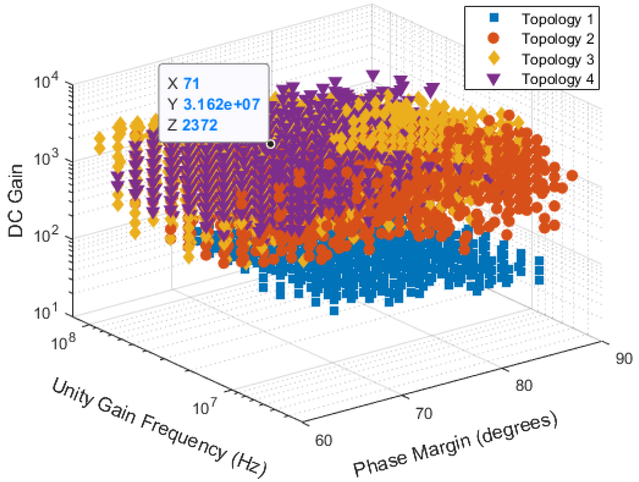
In order to visualize the topology prediction produced by the neural network, we used a test case that considers three important specifications: the DC gain, the phase margin (PM), and the unity-gain frequency (UGF). The predictions of four topologies of circuits are visualized in
Figure 2. These four topologies are common source amplifier, folded cascode amplifier, telescopic cascode amplifier with wide-swing mirror load, and telescopic cascode amplifier with cascode current mirror load, respectively. For each point in the 3D space (i.e., each set of specifications), the neural network predicts the best topology to be used. Additional types of visualizations can be created to help the designer understand the decisions of the prediction network. In addition, the visualizations can be used as a learning tool for students and novice designers.
In order to further illustrate that the topology prediction provided by the network is feasible and can meet all the design specifications, a design point is selected from
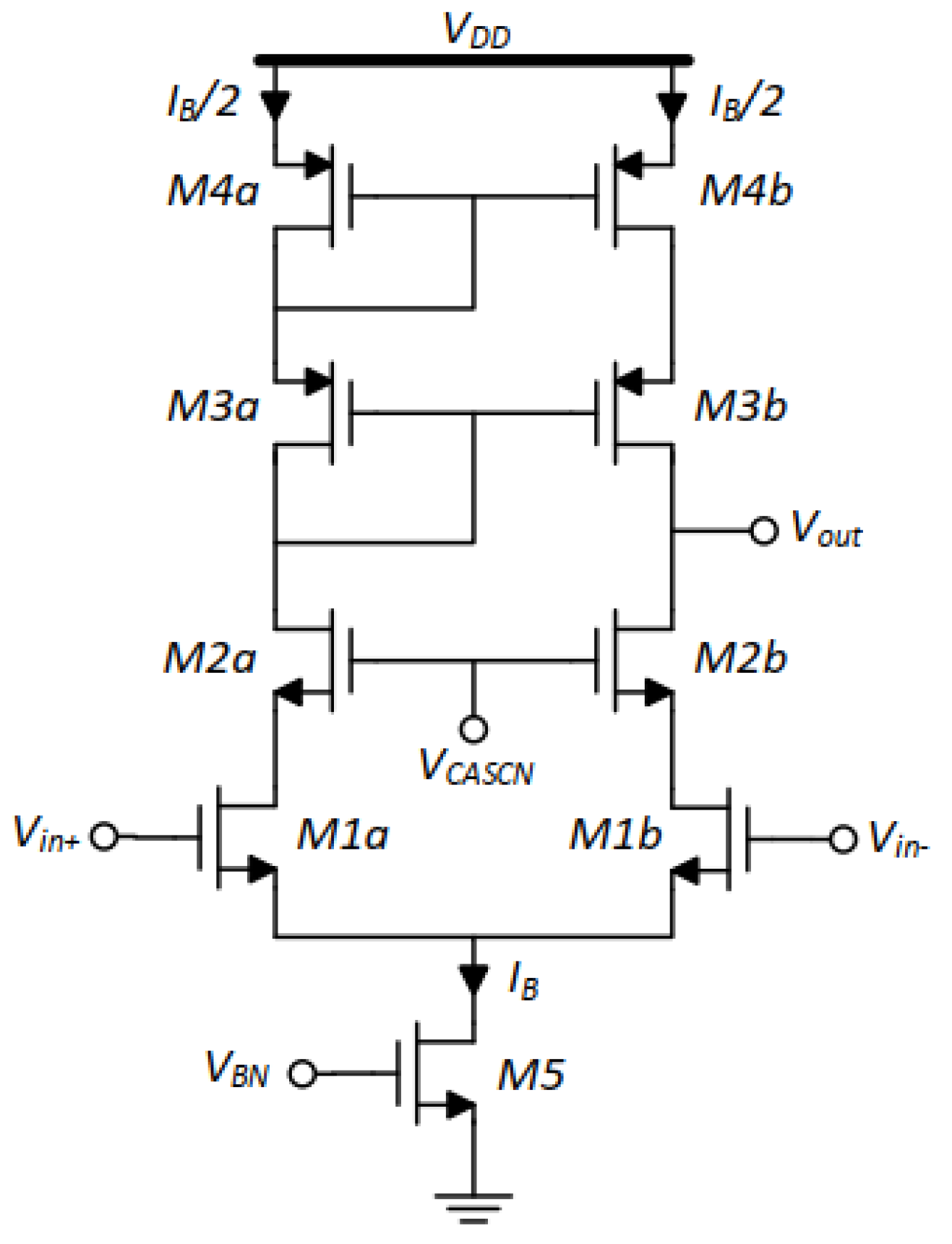
Figure 2 as an example (DC Gain = 67.2 dB, UGF = 31.6 MHz, PM = 71°). The prediction of the network for this design point is topology 4 is shown in
Figure 2. Topology 4 is a telescopic cascode amplifier with telescopic load. The schematic of the predicted topology is shown in
Figure 3.
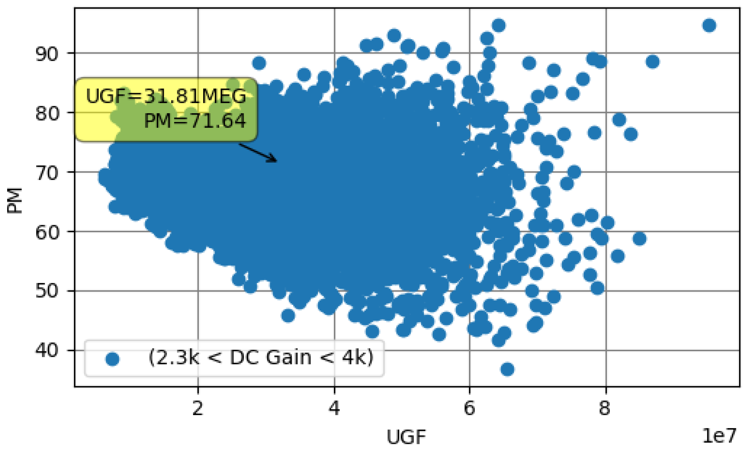
We generated a dataset for the selected topology and visualized it as shown in
Figure 4. The generated dataset indicates that the required design point is indeed feasible using the predicted topology. We used the gm/ID design methodology to size the transistors of the selected topology. The sizing results are shown in
Table 5. The sized circuit was simulated using Cadence specter to verify the circuit specifications. The simulated results are reported in
Table 6 and compared against the input that was provided to the neural network. The comparison reveals that all the required circuit specifications are satisfied, which illustrates that the topology prediction provided by the neural network is appropriate. It should be noted that the effect of process, voltage, and temperature (PVT) variations can be included in the topology selection procedure by using additional datasets generated at PVT corners [
9].
6. Conclusions
This work proposed the automation of analog circuit topology selection using machine learning. A large dataset for 30 different topologies was generated using precomputed lookup tables. The dataset was used to train a neural network, and the network was tested on the testing set. The network achieved an accuracy of 95.4%, and the training time was 2 h. A second approach that was focused on minimizing the total training time was examined. A two-stage prediction process was implemented and achieved an accuracy of 90.8% in one minute of training. The second approach provides a fast and agile solution for topology selection as it gives the designer the flexibility in setting the required specifications with reasonable accuracy while training the network on the fly.
Author Contributions
Conceptualization, K.K., K.Y. and H.O.; Data curation, K.K. and K.Y.; Funding acquisition, H.O.; Investigation, K.K. and H.O.; Methodology, K.K., K.Y. and H.O.; Project administration, K.Y. and H.O.; Resources, K.K., K.Y. and H.O.; Software, K.K., K.Y. and H.O.; Supervision, H.O.; Validation, K.K., K.Y. and H.O.; Visualization, K.K., K.Y. and H.O.; Writing—original draft, K.K.; Writing—review and editing, K.Y. and H.O. All authors have read and agreed to the published version of the manuscript.
Funding
This research was funded by Egypt’s Information Technology Industry Development Agency (ITIDA) grant number ARP2021.R30.4.
Conflicts of Interest
The authors declare no conflict of interest.
References
- Fayazi, M.; Colter, Z.; Afshari, E.; Dreslinski, R. Applications of Artificial Intelligence on the Modeling and Optimization for Analog and Mixed-Signal Circuits: A Review. IEEE Trans. Circuits Syst. I Regul. Pap. 2021, 68, 2418–2431. [Google Scholar] [CrossRef]
- Rutenbar, R.A.; Gielen, G.; Antao, B. Computer-Aided Design of Analog Integrated Circuits and Systems; IEEE Press: Piscataway, NJ, USA, 2002. [Google Scholar]
- Razavi, B. Design of Analog CMOS Integrate: Circuits, 2nd ed.; McGraw Hill: New York, NY, USA, 2017. [Google Scholar]
- Veselinovic, P.; Leenaerts, D.; Van Bokhoven, W.; Leyn, F.; Proesmans, F.; Gielen, G.; Sansen, W. A flexible topology selection program as part of an analog synthesis system. In Proceedings of the 1995 European Conference on Design and Test, Paris, France, 6–9 March 1995; p. 119. [Google Scholar]
- Torralba, A.; Chavez, J.; Franquelo, L.G. FASY: A fuzzy-logic based tool for analog synthesis. IEEE Trans. Comput. Aided Des. Integr. Circuits Syst. 1996, 15, 705–715. [Google Scholar] [CrossRef]
- Soliman, N.R.; Khalil, K.D.; Abd El Khalik, A.M.; Omran, H. Application of Artificial Neural Networks to the Automation of Bandgap Reference Synthesis. In Proceedings of the 2020 37th National Radio Science Conference, Cairo, Egypt, 8–10 September 2020. [Google Scholar]
- Available online: https://adt.master-micro.com/ (accessed on 1 June 2022).
- Youssef, A.A.; Murmann, B.; Omran, H. Analog IC Design Using Precomputed Lookup Tables: Challenges and Solutions. IEEE Access 2020, 8, 134640–134652. [Google Scholar] [CrossRef]
- Elmeligy, K.; Omran, H. Fast Design Space Exploration and Multi-Objective Optimization of Wide-Band Noise-Canceling LNAs. Electronics 2022, 11, 816. [Google Scholar] [CrossRef]
- Available online: https://www.tensorflow.org/ (accessed on 1 December 2021).
| Publisher’s Note: MDPI stays neutral with regard to jurisdictional claims in published maps and institutional affiliations. |
© 2022 by the authors. Licensee MDPI, Basel, Switzerland. This article is an open access article distributed under the terms and conditions of the Creative Commons Attribution (CC BY) license (https://creativecommons.org/licenses/by/4.0/).


