Abstract
On-chip spiral inductors with variable line width layouts are known for their high quality factor (Q-factor). In this paper, we present an analytical approach to facilitate the design of such inductors. Based on an analysis of ohmic and eddy-current losses, we first derive an analytical formula for the metal resistance calculation of a spiral inductor. By minimizing the metal resistance, a simple design equation for finding the proper line width of each coil is then presented. Several 0.18 μm CMOS spiral inductors are investigated, via electromagnetic simulations and experimental studies, to test the proposed resistance calculation, as well as the variable line width design method. It is found that the developed resistance calculation can effectively model the metal-line resistance of a spiral inductor. Moreover, the inductor with a variable line width obtained using the proposed method can significantly improve the Q-factor with little compromise to inductance, which validates the capacity of the developed variable line width design technique. Since the proposed approach can be carried out using analytical calculations, it may be a more efficient design method than those previously reported in the literature.
1. Introduction
With the rapid growth of the demand for low-power, low-cost, and high-integration wireless communication systems, the development of on-chip passive devices for Si-based radio frequency integrated circuits (RFICs) has recently emerged as a critical issue. Among the passive circuit designs, on-chip spiral inductors are particularly important and widely used in RFICs, such as mixers, low-noise amplifiers (LNAs), and voltage-controlled oscillators (VCOs). There has been much research on the analysis and design of RFIC spiral inductors. One important issue of concern in the design of a spiral inductor is the improvement of the quality factor (Q-factor). This is particularly critical for square spirals, which exhibit higher chip-area efficiency but a lower Q-factor than circular and octagonal spirals. It is well known that the Q-factor of a Si-based spiral inductor is mainly determined by three technology parameters: (1) the resistive loss of the metal line, (2) the substrate loss of the silicon buck, and (3) the parasitic capacitance of the insulating oxide layers. By using advanced micromachining technologies, various novel spiral structures have been proposed to alleviate the loss of silicon substrate and the parasitic oxide capacitance [1,2,3,4,5,6,7,8,9,10,11,12,13]. In general, these designs can greatly improve the Q-factor of RFIC inductors, but they can be much more expensive than designs using standard silicon technology. Moreover, it may be more difficult to reliably integrate these micromachined spiral inductors with other components and circuits.
However, reducing the resistive loss of the metal line is a more practical approach to improving the Q-factor. In spiral inductors, metal losses can be attributed to two effects. One is the intrinsic ohmic loss of the metal conductors and the other is the eddy-current loss due to the eddy current induced by the time-varying magnetic field passing through the metal strips. The ohmic loss can be directly reduced by using a thick metal layer or a high-conductivity metal material. These treatments, nevertheless, increase the cost. Metal losses can be also reduced by minimizing the eddy-current loss. The eddy-current loss exists because the time-varying magnetic field supported by the inductor induces the eddy current on the metal strip. Due to the induced eddy current, the net current distribution on the metal strip concentrates on the inner edge of the strip and, thus, increases the metal resistance. To mitigate the influence of the eddy current, inductor designs with variable line widths and/or line spacing layouts have been presented [14,15,16,17,18,19,20,21,22,23,24,25]. Figure 1 shows the layout of a spiral inductor with a variable line width design. In the modified design, the inner coils, that is, the metal strips near the center of the inductor, where the magnetic field intensity and, thus, the eddy-current effect is relatively influential, are designed to have a narrower line width to minimize the eddy-current loss. On the contrary, the metal loss of the outer coils is mostly governed by the ohmic loss since only a slight magnetic field passes the outer metal lines. The outer coils are therefore designed to have a wider line width to reduce the ohmic loss. With the variable line width design, high Q-factor spiral inductors can be developed and applied to improve the performances of various RFICs, such as LNAs and VCOs [21,25].
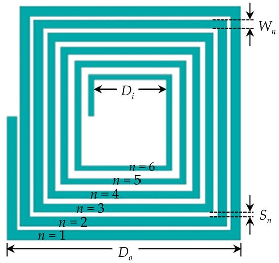
Figure 1.
A modified spiral inductor design with variable metal line width.
Although the variable line width design can effectively improve the inductor Q-factor, it can also complicate the design of the layout. Refs. [14,15] adopted an iterative calculation to optimize the layout. Refs. [16,17,18,19,20,22,24] analyzed numerous spirals with different geometrical parameters and performed data comparison to obtain the design results. Refs. [23,25] used CAD optimization tools to design inductors without considering metal resistance. Ref. [21] developed an analytical algorithm based on ohmic resistance to design the line width of each coil. In this work, a more efficient design approach, which can be carried out using analytic calculations, is developed to facilitate the design of spiral inductors with variable line widths. For a spiral inductor, we first derive an analytical calculation of the resistance of each metal coil based on an analysis of the ohmic and eddy-current losses. By minimizing the metal resistance, a simple analytical design equation for finding the proper line width is then presented. Table 1 briefly compares the proposed approach with related studies reported in the previous literature. To test the proposed resistance calculation, as well as the variable line width inductor design method, several 0.18 μm CMOS spiral inductors are investigated using electromagnetic simulations and experimental studies. It is found that the proposed resistance calculation can effectively model the frequency response of the metal resistance of a spiral inductor. Meanwhile, the developed variable line width design approach can significantly improve the Q-factor with little compromise to inductance. Finally, a good agreement between the simulated and measured data is observed, indicating the validation and capability of the presented design method.

Table 1.
A comparison of studies on the analysis of spiral inductors with variable metal line widths.
2. Design Method
The layout of the inductor design investigated in this work is shown in Figure 1, where the line width of the metal coils is broadened from inner to outer turns. To derive the metal resistance calculation and line width design equation, we denote the number of metal coils from the most outer turn as n = 1, the next turn as n = 2, etc., until reaching the most inner turn as shown in Figure 1. Then, the power dissipation in the n-th metal coil can be written as
where is the excitation current, and and are the total and ohmic resistances of the n-th metal coil, respectively. is the resistance due to the eddy current flowing in the n-th coil. Notice that and are magnetically induced quantities, and they are determined by the excitation current . In addition, can be readily found from Ohm’s law and given by
where and are the length and width of the n-th coil, respectively, and denotes the sheet resistance, with σ being the metal conductivity and T being the metal strip thickness.
In order to find the magnetically induced eddy-current loss , the treatment reported in [26,27,28,29] is adopted here. Following the first-order approximation [27], the magnitude of the eddy current density near the trace edges can be estimated as
where ω and are the angle frequency and the permeability of free space, respectively. Pn is the turn pitch, N is the total number of turns, and M is the turn number where the magnetic field falls to zero and reverses direction. In addition, the eddy current is concentrated near the edges of the metal strip only within an effective width, which can be reasonably regarded as the skin depth [27,28,29]. The eddy current Ieddy,n and the resistance Reddy,n are therefore given by
Substituting Equations (2)–(4) into Equation (1), the total resistance of the n-th metal coil Rt,n is then derived as
From Equation (5), the total metal resistance of a spiral inductor can be calculated:
Equation (5) indicates that, while the ohmic resistance is inversely proportional to Wn, the resistance due to the eddy current (the second term of Equation (5)) is proportional to . A similar observation can be found in [14,15,16,17]. To find the proper line width that can minimize the metal resistance, the differential of Rt,n with respect to Wn in Equation (5) is set to zero, which leads to
Finally, if we choose M = N/4, as suggested in [26], the line width design Equation (7) can be further simplified and written in a concise way as
where Do and Di are the outer and inner diameters of the inductor, respectively.
Using the line width design Equation (8), the design procedures of a spiral inductor with a variable line width are summarized as follows:
- 1.
- For a specified inductance and operating frequency, the design of a conventional inductor with a fixed line width can be obtained first. The obtained Do, Di, N, and Wn values are then used as the reference geometry parameters for the variable line width inductor design.
- 2.
- As the inductance is mainly subject to Do, Di, and N, these three parameters of the variable line width inductor are designed to be identical to the reference geometry parameters in step 1 to maintain the required inductance value.
- 3.
- For the n-th coil with the number of n being larger than (where denotes the ceiling function), the line width is modified using Equation (8). The remaining outer coils are designed to have the same line width as that of the reference design in step 1, since the eddy-current effect is less significant on the outer coils.
3. Results and Discussion
To examine the improvement achieved by the proposed design technique, three six-turn rectangular spiral inductors with an identical outer diameter of 160 μm are investigated and compared. These inductors are designed using 0.18 μm silicon CMOS technology with a 2 μm top metal thickness, and their layout parameters are listed in Table 2. Inductor L1 is a conventional design with a fixed line width, while L2 and L3 are the modified counterparts of L1 developed using the variable line width design techniques presented in our work and in [21], respectively. Notice that the turn pitch of inductor L2 is kept unchanged, while L3 is designed with a fixed line spacing. Inductors L1, L2, and L3 are analyzed using the EM simulator IE3D to generate S- and Y-parameters, from which the series inductance Ls = Imag[−1/ωY12], series resistance Rs = Real[−1/Y12], and quality factor Q = Imag[−1/Y11]/Real[1/Y11] are extracted. In the following, the applicability of the resistance calculation, that is, Equations (5) and (6), is verified first. The performances of inductors L1, L2, and L3 are then simulated and compared to reveal the capability of the proposed design method. Finally, inductors L1 and L2 are fabricated and measured to experimentally validate the proposed design.
Table 2.
Layout parameters of the tested inductors.
To examine the resistance calculation of a spiral inductor using Equations (5) and (6), as well as the effect of the eddy current, the resistances of inductors L1 and L2 are analyzed and compared. Figure 2a shows the series resistance Rs extracted from the EM simulation of the inductors, and Figure 2b presents the metal-line resistance Rt calculated using Equations (5) and (6).
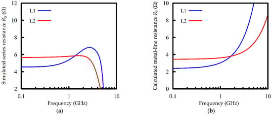
Figure 2.
The frequency responses of the resistances of inductors L1 and L2. (a) The simulated series resistances Rs; (b) the calculated metal-line resistance Rt.
For a Si-based spiral inductor, it has been reported that the series resistance Rs extracted from the network Y-parameter (Rs = Real[−1/Y12]) is mainly determined by the resistance of the metal line at low frequencies. At higher frequencies, however, the parameter Y12 would be significantly influenced by the effects of the oxide capacitance and Si-substrate losses, resulting in a rapid drop in Rs as the frequency increases [1,2,3]. This effect can be observed in Figure 2a at frequencies near and higher than 2.5 GHz. At the same time, Equations (5) and (6) are applicable for the calculation of metal-line resistance. The calculated Rt would thus increase monotonously with an increase in frequency (see the second term of Equation (5)) as demonstrated in Figure 2b. The frequency responses of the computed Rt therefore gradually deviate from the extracted Rs as the frequency increases beyond about 2.5 GHz.
In the low-frequency band (below 2.5 GHz for the tested examples), the variation in Rt with frequency is comparable to that in Rs. Both of them model the metal resistance. Comparing Figure 2a with Figure 2b, Rs is found to be somewhat larger than Rt by about 2 ohms, which may stem from the discontinuity effects at the corners of the coil route. However, their variations with frequencies are quite similar. At frequencies below about 0.5 GHz, where the frequency-invariant ohmic resistance is dominant, Rt and Rs of both inductors L1 and L2 are observed to be nearly independent of frequency. Notice that L2 has a higher resistance than L1 at the low-frequency limit, as the inner coils of L2 are designed with a narrower line width, which leads to the higher ohmic resistance. As the frequency goes beyond 0.5 GHz (and below 2.5 GHz), the effects of the eddy currents become apparent, and the resistances (both Rt and Rs) of the fixed-line-width inductor L1 thus increase rapidly with the increase in frequency. In contrast, the inductor L2 designed with a variable line width is less affected by the eddy-current effects; the resistances of L2 hence increase very slightly over the low-frequency band below 2.5 GHz.
To reveal the performances of the inductor designed using the presented variable line width design technique, we compare the simulated inductance and Q-factor of the tested samples L1, L2, and L3 in Figure 3. It is observed that both L2 and L3, which are designed using variable line widths, can effectively improve the Q-factor with only little compromise to inductance. The inductance values of the variable-line-width inductors L2 and L3 deviate from that of the convention inductor L1 by less than 5% in the frequency band of 1 GHz–15 GHz. Meanwhile, the maximum Q-factors of L2 and L3 are better than that of L1 by about 15 % at 4 GHz. It is also observed that the inner diameter of inductor L3 (which is designed using the method reported in [21]) must be appropriately adjusted to mitigate the degradation of the inductance, whereas the coil pitch and inner diameter of L2 are exactly the same as those of the conventional inductor L1. Our approach can therefore make the variable line width design more practical.
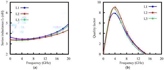
Figure 3.
The simulated performances of inductors L1, L2, and L3. (a) The simulated series inductance Ls; (b) the simulated Q-factor.
To allow for experimental verification, inductors L1 and L2 are fabricated and measured. The die photos of the tested inductors are shown in Figure 4. These inductors are implemented in the 0.18 μm 1P6M CMOS process. Spirals with metal thicknesses of 2 μm are fabricated on the metal six layer, and the underpass is located on the metal five layer. The substrate resistivity is about 10 Ω cm. An on-wafer measurement is carried out by probing the inductors with a probe station and using an Agilent 8510C network analyzer over a frequency range from 100 MHz to 20 GHz. Moreover, the measured raw data are de-embedded with a two-step (open and short) procedure [30,31] to remove the undesired pad parasitics. Figure 5 compares the measured inductance and Q-factor of these two inductors. In addition, Table 3 summarizes the results at some typical frequencies, i.e., 1.8, 2.4, 3.5, and 5.2 GHz. In Table 3 and a comparison between Figure 3 and Figure 5, reasonable agreements can be observed between the measurements and simulations. It is found that, while there is a slight discrepancy between the inductances of L1 and L2, the proposed inductor design L2 can greatly improve the Q-factor performance in the frequency band from about 1.2 to 14 GHz. Meanwhile, the maximum Q-factors of L2 and L1 can be observed at about 3.3 GHz, which are 8.74 and 6.45, respectively. There is 35.5% improvement in the Q-factor performance when using the proposed modified inductor design.
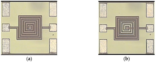
Figure 4.
The die photos of the measured inductors. (a) The fixed-line-width inductor L1; (b) the variable-line-width inductor L2.
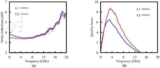
Figure 5.
The measured performances of inductors L1 and L2. (a) The measured series inductance Ls; (b) the measured Q-factor.
Table 3.
A comparison of the performances of inductors L1 and L2 at typical frequencies.
4. Conclusions
The metal resistance, due to the ohmic and eddy-current losses, of an on-chip spiral inductor was calculated and analyzed. From the comparison between the computed results and EM simulations, it was found that the derived resistance calculation can appropriately model the metal resistance of an inductor. By minimizing the metal resistance, an analytic design technique for a spiral inductor with a variable line width was developed. It was found that the inductor with a variable line width designed using the proposed design method can significantly improve the Q-factor with little compromise to inductance. A good agreement between the simulated and measured data was observed, indicating the validation and capability of the developed design method.
Author Contributions
Conceptualization, H.-H.C. and Y.-W.H.; methodology, H.-H.C. and Y.-W.H.; theoretical formulation, H.-H.C.; simulation analysis, H.-H.C.; experimental investigation, H.-H.C. and Y.-W.H.; writing—original draft preparation, H.-H.C.; writing—review and editing, H.-H.C. and Y.-W.H.; project administration, H.-H.C. and Y.-W.H. All authors have read and agreed to the published version of the manuscript.
Funding
This research was funded in part by CviLux Corp., New Taipei City, Taiwan, grant number 111WA00117, 111AA0005.
Data Availability Statement
The data presented in this study are available on request from the corresponding author.
Conflicts of Interest
The authors declare no conflict of interest.
References
- Burghartz, J.N.; Rejaei, B. On the design of RF spiral inductors on silicon. IEEE Trans. Electron Devices 2003, 50, 718–729. [Google Scholar] [CrossRef]
- Yue, C.; Wong, S. Physical modeling of spiral inductors on silicon. IEEE Trans. Electron Devices 2000, 47, 560–568. [Google Scholar] [CrossRef]
- Lee, C.-Y.; Chen, T.-S.; Deng, J.-S.; Kao, C.-H. A simple systematic spiral inductor design with perfected Q improvement for CMOS RFIC application. IEEE Trans. Microw. Theory Tech. 2005, 53, 523–528. [Google Scholar] [CrossRef]
- Chen, T.-S.; Deng, J.-S.; Lee, C.-Y.; Kao, C.-H. Improved performance of Si-based spiral inductors. IEEE Microw. Wirel. Components Lett. 2004, 14, 466–468. [Google Scholar] [CrossRef]
- Lakdawala, H.; Zhu, X.; Luo, H.; Santhanam, S.; Carley, L.; Fedder, G. Micromachined high-Q inductors in a 0.18-μm copper interconnect low-k dielectric CMOS process. IEEE J. Solid-State Circuits 2002, 37, 394–403. [Google Scholar] [CrossRef]
- Hikmat, O.F.; Ali, M.S.M. RF MEMS Inductors and Their Applications—A Review. J. Microelectromech. Syst. 2017, 26, 17–44. [Google Scholar] [CrossRef]
- Büyüktas, K.; Koller, K.; Müller, K.-H.; Geiselbrechtinger, A. A New Process for On-Chip Inductors with High Q-Factor Performance. Int. J. Microw. Sci. Technol. 2010, 2010, 517187. [Google Scholar] [CrossRef][Green Version]
- Han, M.; Wang, S.F.; Xu, G.W.; Luo, L. Suspended high Q integrated inductor by wafer level packaging technology. Microsyst. Technol. 2015, 21, 215–219. [Google Scholar] [CrossRef]
- Kifle, T.; Chandra, S.; Koul, S.K. A novel fabrication process for MEMS spiral inductors realized on oxide islands. Microsyst. Technol. 2015, 21, 1415–1422. [Google Scholar] [CrossRef]
- Ding, Q.; Shi, Y.; Li, X. Quality factor enhancement of spiral inductors with patterned trench isolation. In Proceedings of the 10th IEEE International Conference Solid-State Integration Circuit Technology, Shanghai, China, 1–4 November 2010; pp. 731–733. [Google Scholar] [CrossRef]
- Yang, M.-Z.; Dai, C.-L.; Hong, J.-Y. Manufacture and Characterization of High Q-Factor Inductors Based on CMOS-MEMS Techniques. Sensors 2011, 11, 9798–9806. [Google Scholar] [CrossRef]
- Bhaskar, A.; Philippe, J.; Avramovic, V.; Braud, F.; Robillard, J.-F.; Durand, C.; Gloria, D.; Gaquiere, C.; Dubois, E. Substrate Engineering of Inductors on SOI for Improvement of Q-Factor and Application in LNA. IEEE J. Electron Devices Soc. 2020, 8, 959–969. [Google Scholar] [CrossRef]
- Le, H.T.; Haque, R.I.; Ouyang, Z.; Lee, S.W.; Fried, S.I.; Zhao, D.; Qiu, M.; Han, A. MEMS inductor fabrication and emerging applications in power electronics and neurotechnologies. Microsyst. Nanoeng. 2021, 7, 59. [Google Scholar] [CrossRef]
- Lopez-Villegas, J.; Samitier, J.; Cane, C.; Losantos, P.; Bausells, J. Improvement of the quality factor of RF integrated inductors by layout optimization. IEEE Trans. Microw. Theory Tech. 2000, 48, 76–83. [Google Scholar] [CrossRef]
- Shen, P.; Zhang, W.; Huang, L.; Jin, D.; Xie, H. Improving the quality factor of an RF spiral inductor with non-uniform metal width and non-uniform coil spacing. J. Semicond. 2011, 32, 064011. [Google Scholar] [CrossRef]
- Kobe, O.B.; Chuma, J.M.; Jamisola, R.S.; Chose, M. Modeling high-Q square spiral with variable segment width and spacing. In Proceedings of the 2016 IEEE Radio and Antenna Days of the Indian Ocean (RADIO), Reunion, France, 10–13 October 2016; pp. 1–2. [Google Scholar] [CrossRef]
- Liu, J.; Shi, Y.; Wen, X.; Chen, D.; Luo, T.-X.; Huang, H.; Ye, H.; Wang, Y. On-chip spiral inductor with novel gradually changed structure. Microw. Opt. Technol. Lett. 2008, 50, 2210–2213. [Google Scholar] [CrossRef]
- Tayenjam, S.; Vanukuru, V.; Sundaram, K. High-Q Variable Pitch Spiral Inductors for Increased Inductance Density and Figure-of-Merit. IEEE Trans. Electron Devices 2019, 66, 4481–4485. [Google Scholar] [CrossRef]
- Vanukuru, V.N.R.; Chakravorty, A. High-Q Characteristics of Variable Width Inductors with Reverse Excitation. IEEE Trans. Electron Devices 2014, 61, 3350–3354. [Google Scholar] [CrossRef]
- Vanukuru, V.N.R. High-Q Inductors Utilizing Thick Metals and Dense-Tapered Spirals. IEEE Trans. Electron Devices 2015, 62, 3095–3099. [Google Scholar] [CrossRef]
- Hsu, H.-M.; Chan, K.-Y.; Chien, H.-C.; Kuan, H.-C. Analytical Design Algorithm of Planar Inductor Layout in CMOS Technology. IEEE Trans. Electron Devices 2008, 55, 3208–3213. [Google Scholar] [CrossRef]
- Hsu, H.-M. Improving the quality factor of a broadened spiral inductor with arithmetic-progression step width. Microw. Opt. Technol. Lett. 2008, 45, 118–120. [Google Scholar] [CrossRef]
- Elhajjami, I.; Benhala, B.; Bouyghf, H. Optimal Design of RF Integrated Inductors via Differential Evolution Algorithm. In Proceedings of the 2020 1st International Conference Innovative Research in Applied Science Engineering and Technology (IRASET), Meknes, Morocco, 16–19 April 2020; pp. 1–6. [Google Scholar] [CrossRef]
- Royet, A.S.; Michel, J.P.; Reig, B.; Pornin, J.L.; Ranaivoniarivo, M.; Robain, B.; de Person, P.; Uren, G. Design of optimized high Q inductors on SOI substrates for RF ICs. In Proceedings of the 2016 IEEE International Conference on Electronics, Circuits and Systems (ICECS), Monte Carlo, Monaco, 11–14 December 2016; pp. 324–327. [Google Scholar] [CrossRef]
- Manikandan, R.R.; Vanukuru, V.N.R.; Chakravorty, A.; Amrutur, B. Design and modeling of high-Q variable width and spacing, planar and 3-D stacked spiral inductors. In Proceedings of the 18th International Symposium on VLSI Design and Test, Coimbatore, India, 16–18 July 2014; pp. 1–6. [Google Scholar] [CrossRef]
- Kuhn, W.; Ibrahim, N. Analysis of current crowding effects in multiturn spiral inductors. IEEE Trans. Microw. Theory Tech. 2001, 49, 31–38. [Google Scholar] [CrossRef]
- Ooi, B.-L.; Xu, D.-X.; Kooi, P.-S.; Lin, F.-J. An improved prediction of series resistance in spiral inductor modeling with eddy-current effect. IEEE Trans. Microw. Theory Tech. 2002, 50, 2202–2206. [Google Scholar] [CrossRef]
- Tong, K.; Tsui, C. A physical analytical model of multilayer on-chip inductors. IEEE Trans. Microw. Theory Tech. 2005, 53, 1143–1149. [Google Scholar] [CrossRef]
- Zou, W.; Chen, X.; Zou, X. An improved analytical series resistance model for on-chip stacked inductors. In Proceedings of the 2013 IEEE, 10th I&nternational Conference on ASIC, Shenzhen, China, 28–31 October 2013; pp. 1–4. [Google Scholar] [CrossRef]
- Cheng, Y.; Deen, J.; Chen, C.-H. MOSFET Modeling for RF IC Design. IEEE Trans. Electron Devices 2005, 52, 1286–1303. [Google Scholar] [CrossRef]
- Haobijam, G.; Palathinkal, R.P. Design and Analysis of Spiral Inductors; Spinger: New Delhi, India, 2014. [Google Scholar] [CrossRef]
Publisher’s Note: MDPI stays neutral with regard to jurisdictional claims in published maps and institutional affiliations. |
© 2022 by the authors. Licensee MDPI, Basel, Switzerland. This article is an open access article distributed under the terms and conditions of the Creative Commons Attribution (CC BY) license (https://creativecommons.org/licenses/by/4.0/).