Article

A 0.0012 mm2 6-bit 700 MS/s 1 mW Calibration-Free Pseudo-Loop-Unrolled SAR ADC in 28 nm CMOS

School of Electrical Engineering, Korea Advanced Institute of Science and Technology (KAIST), Daejeon 34141, Korea
*
Author to whom correspondence should be addressed.
Electronics 2022, 11(11), 1707; https://doi.org/10.3390/electronics11111707
Submission received: 25 April 2022 / Revised: 22 May 2022 / Accepted: 25 May 2022 / Published: 27 May 2022
(This article belongs to the Section Circuit and Signal Processing)

Abstract

:
This paper presents a high-speed successive approximation register (SAR) analog-to-digital converter (ADC) that takes advantage of both asynchronous SAR ADC and loop-unrolled (LU) SAR ADC. By utilizing the output of the dynamic amplifier (DA) to generate an asynchronous clock, the reset time for the DA can be hidden behind the comparator latching time. Dedicated latches for each digital-to-analog converter (DAC) element eliminate the need for DAC switching logic. The proposed inverter-inserted three-stage comparator significantly reduces the input-referred offset of the comparator. The prototype 6-bit 700 MS/s SAR ADC was implemented in a 28 nm CMOS process and has a small 0.0012 mm2 area. The measured peak DNL and INL without any mismatch calibration were 0.33 and 0.27 LSB, respectively. With Nyquist input, the measured signal-to-noise and distortion ratio (SNDR) and spurious-free dynamic range (SFDR) were 34.07 and 47.52 dB, respectively. The power consumption was 1 mW under a supply voltage of 1.0 V, leading to a Walden figure of merit (FoM) of 34.6 fJ/conversion-step at 700 MS/s.

1. Introduction

The high-speed communication systems such as ADC-based transceivers for high-speed I/O standards using four-level pulse modulation (PAM-4) required low-resolution (6–8 bit) and tens of GS/s time-interleaved (TI) ADC [1,2,3]. The performance of these systems is greatly affected by the characteristics of input bandwidth, sampling rate, effective resolution, power consumption, and area of the TI ADC. In order to realize a low-power TI ADC of several tens of GS/s, a single channel ADC used as a sub-ADC must be designed to be very compact and high-speed. During the past decade, successive approximation register (SAR) analog-to-digital converters (ADCs) have become a dominant ADC architecture as sub-ADCs of the TI ADC, covering a wide range of resolution and speed owing to advanced process technologies, mostly attributed to their digital friendly architecture [4,5,6,7,8,9,10,11]. The need for high-speed clocks for internal loop operation in a synchronous SAR ADC can be eliminated by using asynchronous architecture [12,13,14]. It could even make the conversion speed faster, because the next comparison can be conducted as soon as the previous decision is completed, without the need to wait for the next clock. Nevertheless, the logic delay, due to the digital-to-analog converter (DAC) control, and the comparator reset time needed for every decision cycle, due to the repeatedly used single comparator, create a fundamental speed bottleneck for asynchronous SAR ADC. The time spent for the repeated reset and DAC control can be eliminated by unrolling the loop with an architecture of so-called loop-unrolled (LU) SAR, which uses as many comparators as the ADC resolution [15,16,17,18,19,20,21]; accordingly, the conversion speed can be further enhanced. However, the major drawbacks of the LU SAR ADC are offset mismatches among the multiple comparators, which require burdensome offset calibration with a foreground [15,16,17] or background using an additional comparator [18,19,20]. Meanwhile, the offset calibration burden could be alleviated by redundancy bits [21]. However, in order to use the redundancy bit, not only is an additional conversion cycle required, but also the design complexity increases, because two different types of ADCs should be used as in [21].
In this paper, we propose a calibration-free pseudo-loop-unrolled (P-LU) SAR ADC architecture that has the speed advantage of an LU SAR ADC without the burden of offset calibration. As the comparator can be designed such that its offset is dominantly determined by the offset of a preamplifier, a single preamplifier can be shared for every decision, as in a conventional SAR ADC. Therefore, the overall area of the ADC can be designed to be compact, without a complex calibration block, and operate with enhanced conversion speed.
This paper is organized as follows. In Section 2, the conventional LU SAR ADC architecture is reviewed. Section 3 describes the architecture of the proposed P-LU ADC. Detailed circuit implementations of the inverter-inserted comparator, the clock generator, and the high-speed logic are explained in Section 4. Section 5 shows the measurement results, and Section 6 concludes the paper.

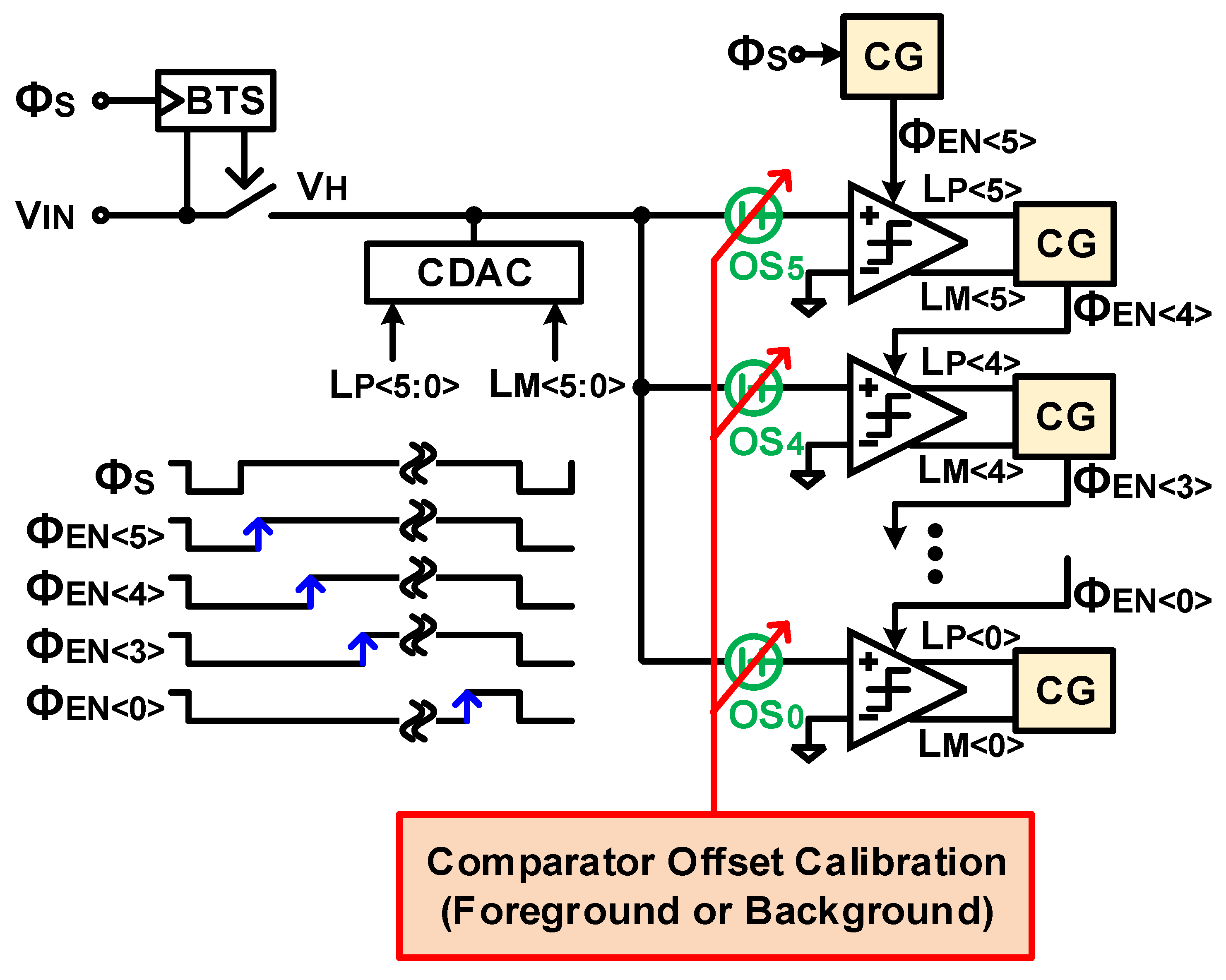
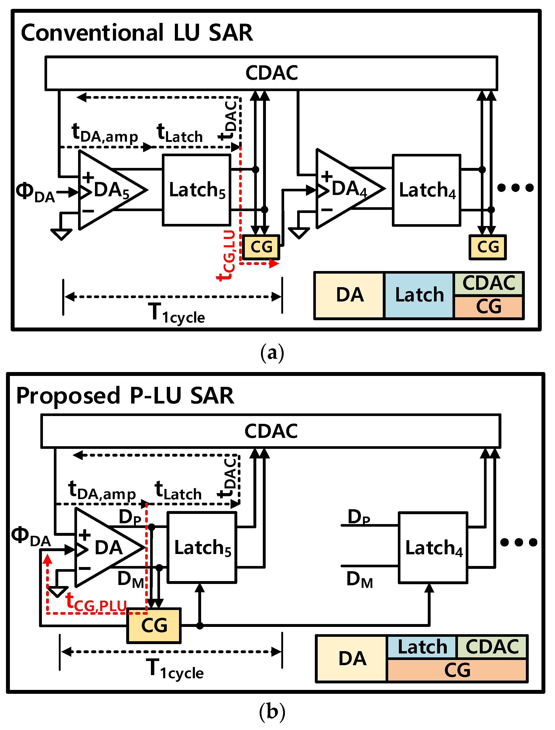
2. Review of LU SAR ADC Architecture

Figure 1 shows a conventional 6-bit LU SAR ADC with six comparators; each of them is dedicated to an individual capacitor for control of the DAC. After the input voltage is sampled by the bootstrapped (BTS) track-and-hold (T/H), the MSB code is obtained by the enable clock ( Φ EN 5 ) synchronized with the external sampling clock ( Φ S ). When the MSB decision is complete, the clocks for the following comparators are generated from their previous comparators, in order, by the clock generation (CG) blocks. This eliminates the need for DAC switching logic or comparator reset time, leaving the essential operations of comparator latching and DAC settling time as the ultimate speed limitation factors, while the need for offset calibration becomes an additional burden, for example, in area and power consumption.
The offset mismatches of the comparators can be calibrated for foreground [15,16,17] and background [18,19,20]. Since the foreground calibration technique requires an additional current cell or capacitor in the comparator, it adversely affects the power consumption and operation speed. In addition, a hardware burden on the area is increased by the addition of logic blocks for detecting and correcting the offset errors. Meanwhile, the offset mismatch of the comparator is changed according to the PVT variations as well as process mismatch. Therefore, for the PVT-insensitive design, the offset mismatch of the comparators inside the LU SAR ADC needs to be calibrated against the background [18,19,20]. The application of the background offset calibration technique affects the conversion speed of the ADC, because it requires additional time for calibration after conversion is complete. In this paper, we propose a calibration-free ADC architecture that can overcome the disadvantages of foreground and background calibration techniques in the previously reported LU SAR ADCs.

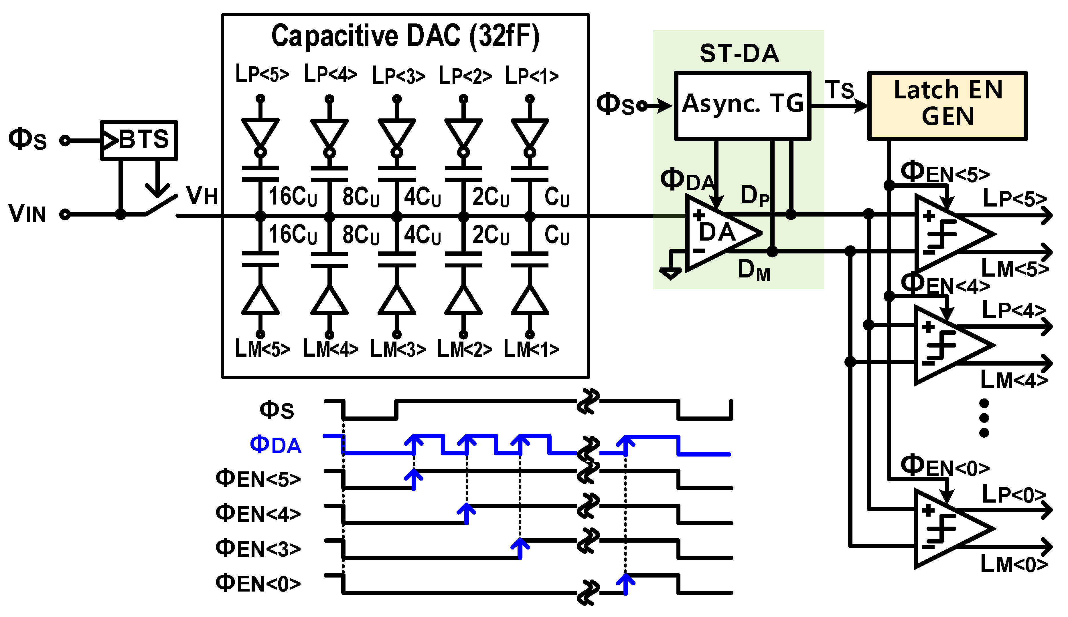
3. Proposed Pseudo-LU SAR ADC

In our design, we want to eliminate the need for offset calibration of the comparator with a single preamplifier while hiding the reset time of the preamplifier behind the essential operations to achieve a conversion speed comparable to that of LU SAR ADCs. With this motivation, the proposed P-LU SAR ADC architecture is shown in Figure 2. The proposed P-LU SAR ADC consists of a T/H, a binary controlled capacitive DAC (CDAC), a self-triggered DA(ST-DA), a Φ EN generator (Latch EN GEN), and six latches. The CDAC is designed with a split-capacitor scheme, as in [22], and the total capacitance of the CDAC is 32 fF with a 0.5 fF unit capacitor. If the switching scheme of the CDAC using a common voltage, VCM, as in [15], is applied to the proposed P-LU SAR ADC, the size of the CDAC can be reduced in half compared to the split-capacitor scheme. However, the switching scheme using VCM increases the design burden on switches and control logics for VCM. On the other hand, the split-capacitor scheme requires only switches for the reference top and bottom voltages. Therefore, the switches for the CDAC can be designed compactly, and can be directly controlled by the differential outputs of the six latches, LP<5:0> and LM<5:0>, as shown in Figure 2. In other words, the logic delay for switching the CDAC is very short. The reset phase (when Φ DA is low, the DP and DM nodes are discharged to ground) and the amplification phase (when Φ DA is high, the DP and DM nodes are charged to VDD) of the DA are determined by the asynchronous timing generator (Async. TG) based on the output signals of the DA (DP and DM). The differential signals amplified by the ST-DA are converted into digital code by each latch synchronized to the rising edge of the Φ DA using the Latch EN GEN as shown in the timing diagram in Figure 2. The operation details of the ST-DA and the Latch EN GEN are covered in Section 4. The proposed ADC has a single ST-DA for pre-amplification and multiple latches dedicated to switching individual DAC elements, as in the LU SAR ADC. Owing to the dedicated latches, the proposed structure does not require reset time for the latches, as in the LU SAR ADC.
Figure 3a shows the critical clock path of the conventional LU SAR ADC using a double-tail comparator [23] in each cycle, which can be expressed as follows.
T 1 cycle = t DA ,   amp + t Latch + max { t DAC ,   t CG ,   LU }
Here, t DA ,   amp , t Latch , t DAC , and t CG ,   LU represent the delay time of DA amplification, the comparator latching, the DAC settling, and the CG logic, respectively. Unlike the conventional LU SAR ADCs, in which the next clock is generated by sensing the output of the latch, this P-LU SAR ADC uses the outputs of the DA for the next clock generation, because the DA outputs can be indicators of the comparator decision state, as in [24], which utilized the DA outputs to avoid metastability. By moving the CG block forward to the input of the latch, as illustrated in Figure 3b, the DA clock generation time ( t CG ,   PLU ) can be hidden behind the latching + DAC settling time ( t Latch + t DAC ) owing to their parallel operation. The cycle of P-LU SAR ADC can be described as follows.
T 1 cycle = t DA ,   amp + t CG ,   PLU t DA ,   amp + t Latch + t DAC
To obtain a speed comparable to that of the LU SAR ADC, the time for DA clock generation ( t CG ,   PLU ) should be designed similar to the time for ( t Latch + t DAC ) as Equation (2). Note that the double-tail comparator combining the DA and latch increases the number of stages over the strong-arm comparator used in the conventional LU SAR ADCs [15,16,17,18,19,20], but it could be designed with a competitive latching time under the condition of low input common voltage [23]. From Equations (1) and (2), the proposed P-LU SAR ADC not only realizes a conversion speed comparable to that of the LU SAR ADCs, but also eliminates the offset calibration burden, which is a disadvantage of the conventional LU SAR ADC. As a result, the proposed ADC can be designed with a competitive conversion speed and a very small area compared to the LU SAR ADCs.
The characteristics and advantages of the proposed P-LU SAR ADC introduced so far are summarized and compared with the previously reported SAR ADCs in Table 1. In the conventional asynchronous SAR ADC [14], the conversion time is increased by the comparator reset time and the DAC switching logic delay. Meanwhile, in the LU SAR ADC [15,16,17,18,19,20,21], the input gate capacitance is increased by the comparator required as much as the resolution (N bits). Furthermore, the hardware burden and current consumption of the ADC are increased by the offset calibration for the comparators [15,16,17,18,19,20]. In the case of LU SAR + SAR ADC using a redundancy bit, an additional conversion cycle is required to obtain the redundancy bit. Moreover, the time for the comparator reset and register operation in the fine stage asynchronous SAR ADC affects the conversion time [21].
In this work, since the proposed P-LU SAR ADC uses only one DA as a preamplifier, it could be designed with a small input gate capacitance without offset calibration such as in the conventional SAR ADC. Moreover, as with the LU SAR ADC, the P-LU SAR ADC can eliminate the effects of the comparator reset time and the DAC switching logic delay. That is, the proposed ADC can be designed as compact, power efficient, and high speed.

4. Circuit Implementation

4.1. Inverter-Inserted Three-Stage Comparator

To discuss the specific timing in our design, we need first to discuss the detailed circuit design of the comparator. To achieve low input-referred offset without calibration despite the wide spread of the offset distribution of the following multiple latches, the preamplifier must provide a sufficiently high gain. In addition, the preamplifier should have enough driving capability for the multiple latches. In this design, therefore, an inverter-inserted three-stage comparator was proposed, consisting of one DA as a preamplifier, six latches for 6-bit conversion, and an inverter stage after the DA to provide sufficient gain and driving strength, as shown in Figure 4a.
Figure 4b shows the timing diagram to explain the operation of the proposed comparator in more detail. In the sampling phase (i.e., Φ S is 0), the DA and six latches were reset. After the input sampling was completed, Φ DA became 1 for amplification and Φ EN 5 was enabled to ready Latch5. In the amplification phase of the DA, DP and DM were charged to VDD with a delay difference. Note that the delay information of the DP and DM nodes was generated by the inverter stage based on the slope difference of SP and SM nodes. Since the inverter stage converted the slope information of the SP and SM nodes into the logic levels, this architecture reduced concern about the latch metastability; then, the final stage worked as digital latches, with enable signals of Φ EN . As the DP and DM nodes were charged to VDD, the MSB code was determined according to the difference in activation time between the input transistors of Latch5. The DAC operation started immediately with the output of Latch5 (LP<5> and LM<5>) and was completed before the next conversion cycle began. Keep in mind that, as mentioned in Section 3, the DA and latches were triggered by DP and DM, except for the MSB conversion cycle. Therefore, after the amplification phase, Φ DA became 0 for reset, and Φ EN 4 was enabled to ready Latch4. This DA-based conversion cycle was repeatedly performed from Latch4 to Latch0 for Φ EN 4 : 0 . The details for the timing generation of Φ DA and Φ EN 4 : 0 are explained in Section 4.2.
As one of the major motivations of the proposed architecture was to reduce the input-referred offset mismatch by the gain of DA, the comparator offset distribution was simulated. Figure 5 shows several histograms of the offset mismatch from the Monte Carlo simulation results with 1000 samples. Figure 5a shows the distribution of the input-referred offset of a conventional strong-arm latch without a preamplifier; the standard deviation was 15 mV. As the differential input range of this ADC was 800 mVdiff, and the 1 LSB voltage was 12.5 mVdiff, the estimated offset distribution could degrade the performance of the ADC. With a DA for preamplification, the standard deviation of the input-referred offset was reduced to 7 mV thanks to the gain of the DA, as shown in Figure 5b. However, when the 3 σ value was considered, it was not sufficiently small. As shown in Figure 4, in the amplification phase, the SP and SM nodes were discharged to ground with different slopes according to the input voltage difference. By inserting an inverter pair between the DA and the six latches as shown in Figure 4, the slope difference of SP and SM nodes was converted into a delay difference by the gain of the inverter. That is, the input difference of the latch following the inverter was increased. As a result, the standard deviation of the input-referred offset was reduced to 1.16 mV, as shown in Figure 5c. Because the 3σ value (3.5 mV) was smaller than 0.5 LSB (6 mV), the proposed ADC did not require any burdensome offset calibration.

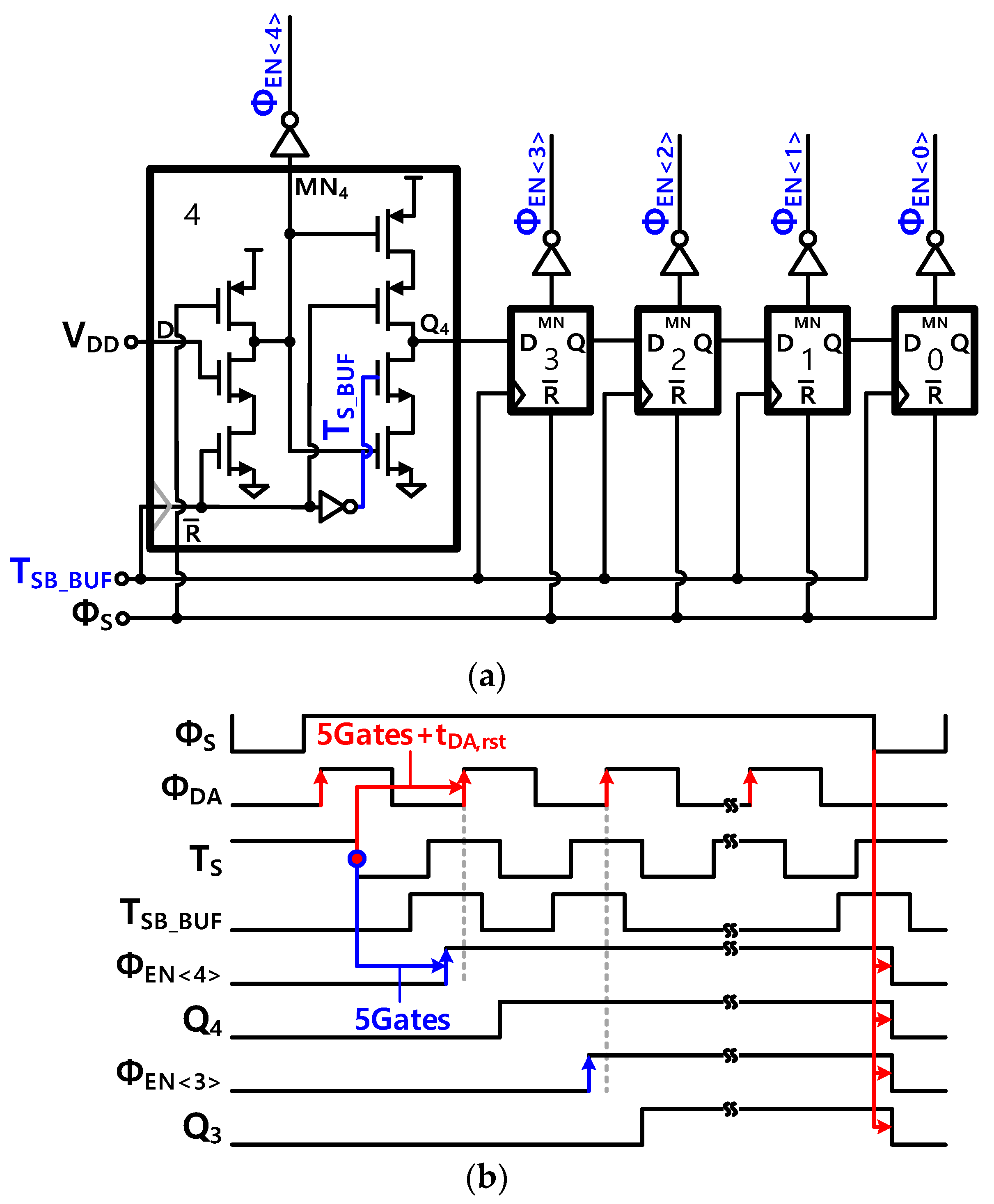
4.2. Clock Generator (CG)

A detailed logic diagram of the CG block for the proposed P-LU SAR ADC architecture and its timing diagram are shown in Figure 6. The CG block generated the clock for DA ( Φ DA ) and the enable signals for the latches ( Φ EN 5 : 0 ). When Φ S changed to 1, Φ DA became 1 for amplification, and Φ EN 5 was enabled to ready Latch5. Then, the DA developed the outputs, DP and DM, with different delays depending on the input, and the TS node became 0 by sensing DP and DM to end the amplification. After a delay of an AND gate, Φ DA fell to 0 to reset the DA (i.e., DP and DM → 0). This made TS node 1, and this triggered the next DA amplification and readied Latch4 with Φ EN 4 = 1 , using the Latch EN GEN. This one cycle of loop operation can be summarized as follows.
T 1 cycle = t DA , amp + t Logic 1 + t DA , rst + t Logic 2
Here, t Logic 1 , t Logic 2 , and t DA , rst represent the time of logic for Φ DA falling, logic for Φ DA rising, and the DA reset, respectively. As t Logic 1 and t Logic 2 are related to Φ DA generation through the same logic gates, they will have almost the same values. Equations (2) and (3) imply that the time for DA clock generation should be designed similar to the time for latching ( t Latch ) + DAC settling ( t DAC ), as in Equation (4).
t Logic 1 + t DA , rst + t Logic 2     t Latch + t DAC
Based on the comparator design shown in Figure 4, let us discuss the actual timing of the decision loop in more detail. Even though the inserted inverters increased t DA , amp and t DA , rst , they could be designed as short as 50 ps and 30 ps, respectively, in nominal condition for our 28 nm process. t Logic 1 ( t Logic 2 ) including NOR and AND gates could be designed within 50 ps. As briefly mentioned earlier, there are two prominent design issues related to the CG block, which are moved to the input of the latch (i.e., DP and DM).
The first issue regards the parallel operation of the DA reset and the comparator latching. It should be guaranteed that the comparator latching completes before the DA reset, as described in Equation (5).
t Logic 1 + t DA , rst   >   t Latch
Certainly, if t Logic 1 + t DA , rst     t Latch then the speed of the loop operation will be degraded. To verify Equation (5) for our design, a simulation was performed with zero input (i.e., VHP = VHM = VCM). Figure 7 shows the timing difference between the DA reset path and the latching path ( Δ T 1 = t Logic 1 + t DA , rst   t Latch ) under supply and temperature variation with 1000 samples. Although the conditions varied, ΔT1 was always positive and guaranteed that the comparator decision was not disturbed by the DA reset.
The second issue is the timing of the latch enable ( Φ EN ): as both DP and DM reach VDD in a short time by DA amplification, the latch should be enabled as soon as the DA operation begins. Unlike the conventional double-tail comparator, in which the turn-on time of the latch should be carefully controlled [23], in our architecture the latch operation begins only after the rise of the inverter outputs, DP and DM (=inputs to the latches), by the DA operation. Therefore, it is enough if Φ EN can be ready earlier than the rising of Φ DA (i.e., Δ T 2   >   0 shown in Figure 6), which provides a sufficient timing margin. Details regarding this follow below.

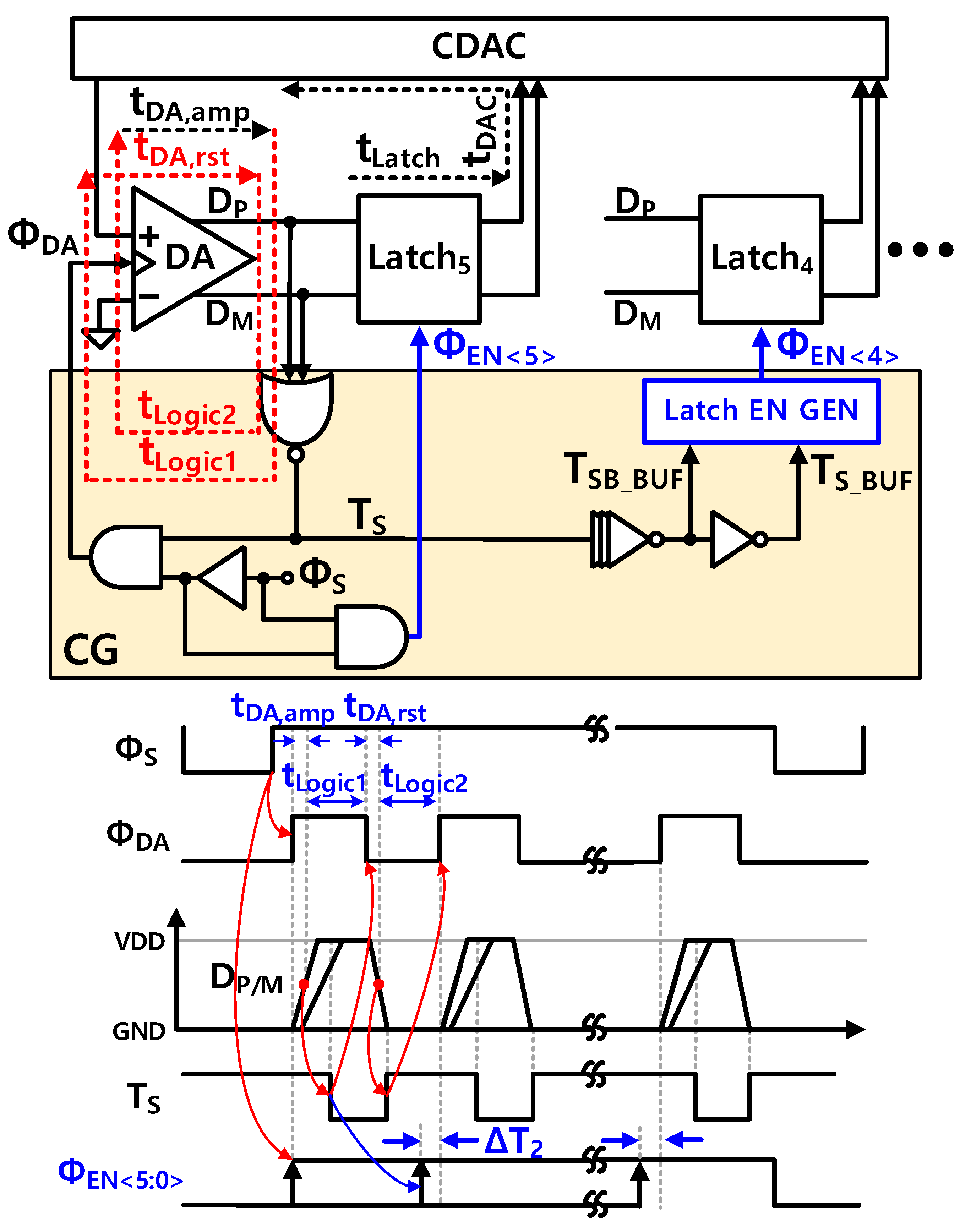
4.3. High-Speed Logic for Latch Enable Generation

Both Φ DA and Φ EN are generated by TS, and they will have different delays. In order to satisfy the condition of Δ T 2   >   0 without speed degradation, the logic for Φ EN generation should be fast. In typical SAR ADCs, Φ EN 5 : 0 is realized with a shift register. A typical true single-phase clock (TSPC) flip-flops; because the number of stages along the clock-to-output path was three or four, the Φ EN generator (Latch EN GEN in Figure 6) was custom-designed as shown in Figure 8a. This circuit included only two stages to generate each Φ EN and enhanced the overall speed of the logic.
The operation of the Latch EN GEN can be explained with its timing diagram, shown in Figure 8b. During Φ S = 0 , all Φ EN 5 : 0 were reset. After sampling ( Φ S = 1 ), if the first DA conversion of the MSB cycle was complete, TS_BUF became 0, and TSB_BUF became 1. Therefore, the MN node of the first block was discharged to GND, and Φ EN 4 was enabled. Starting with the falling edge of T S , the number of logic gates for generating the rising edge of Φ DA was the same as that for generating the rising edge of Φ EN , but the reset time of DA ( t DA ,   rst ) was added to the path of generating Φ DA . Therefore, this design still guaranteed Δ T 2   >   0 . When DA reset again, TS_BUF became 1, and the output (Q) of the first block became 1 to make Φ EN 3 ready. By repeating this operation, each Φ EN for SAR conversion was generated. With the designed clock path and the proposed inverter-inserted three-stage comparator, the design condition of Δ T 2   >   0 was verified.
Figure 9 provides the simulation results of Δ T 2 with 1000 samples. Despite the supply and temperature variation, Δ T 2 was always positive and larger than 5 ps. This means that each Φ EN was ready earlier than the rising of Φ DA , as desired.

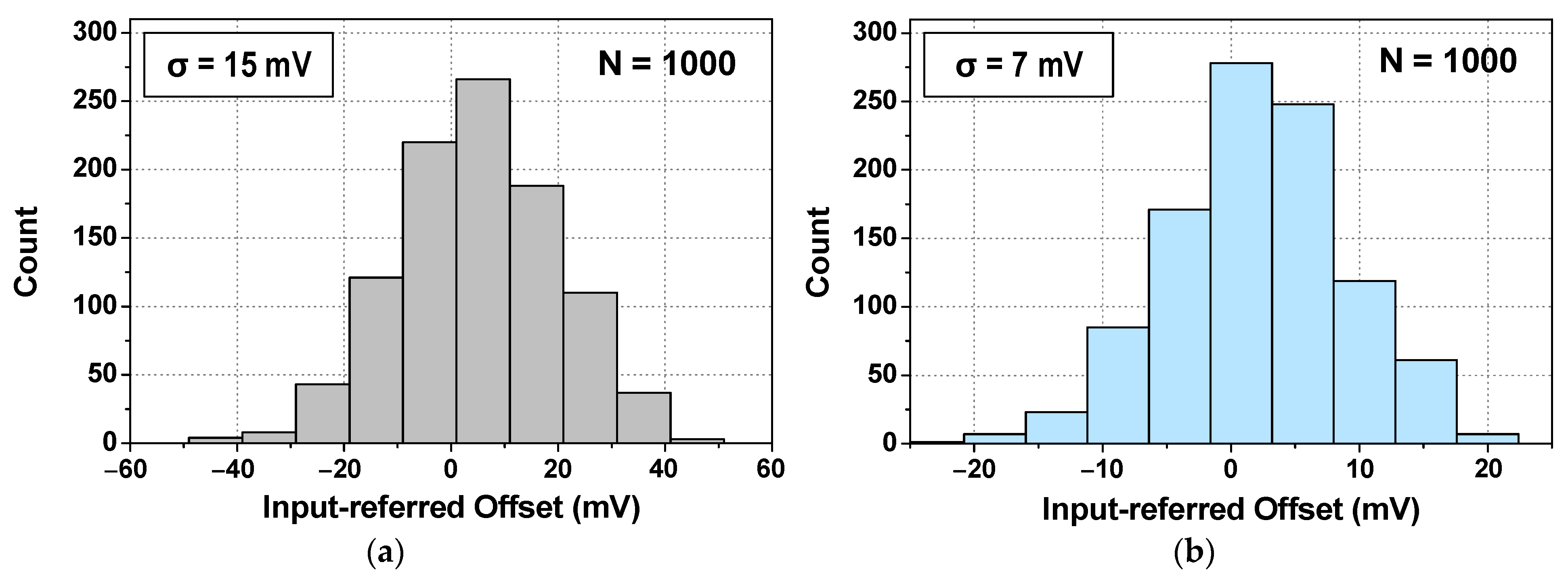
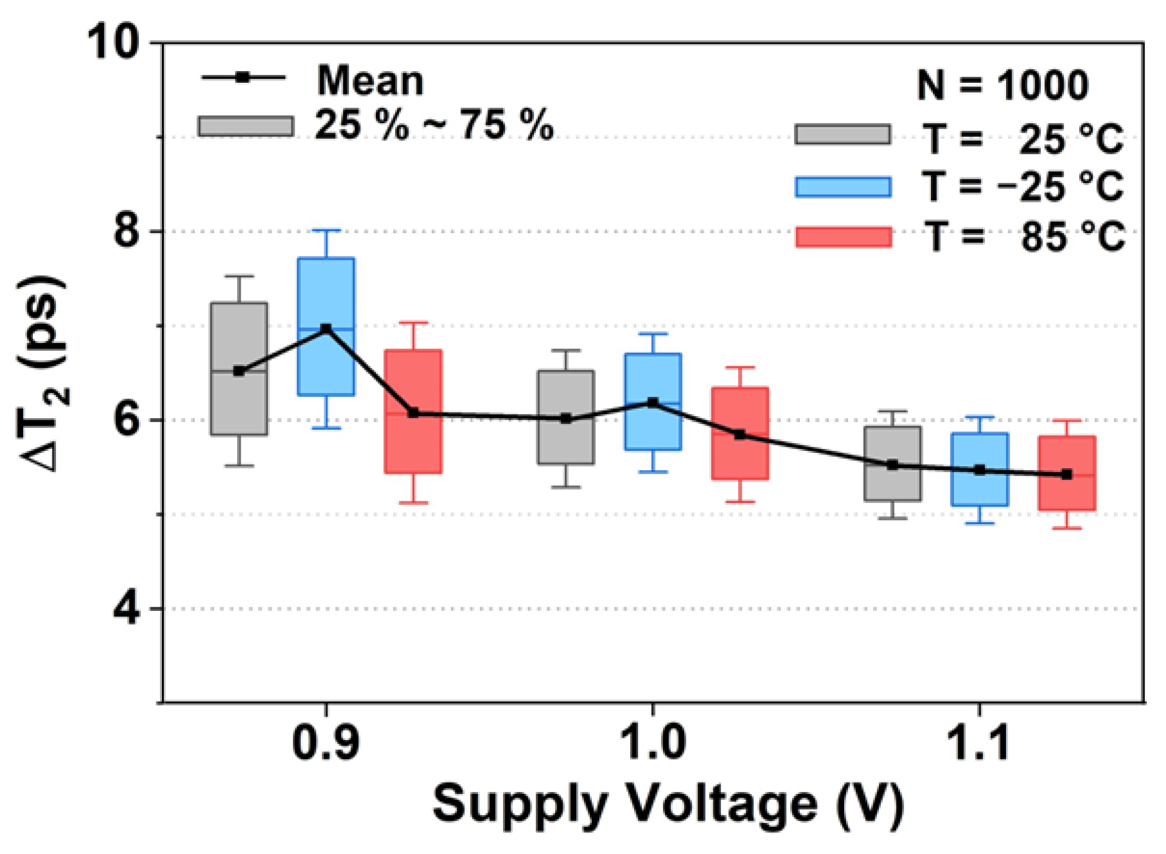
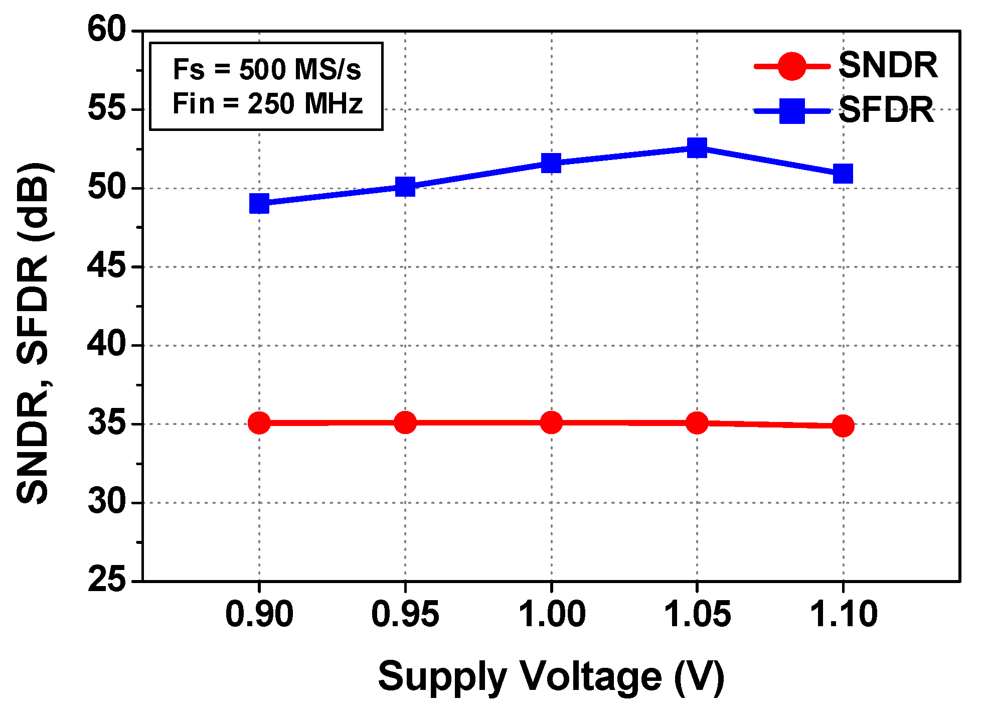
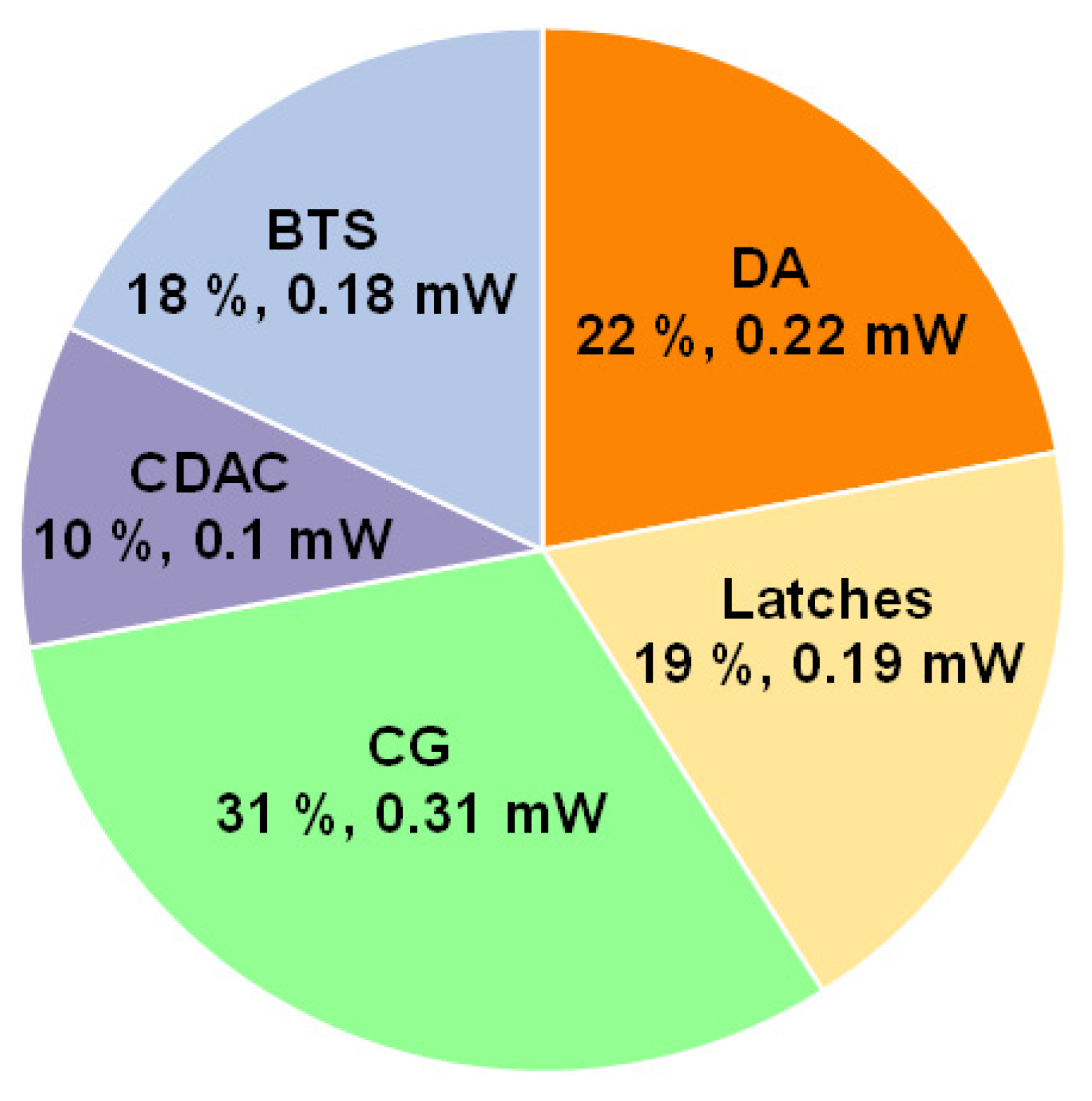
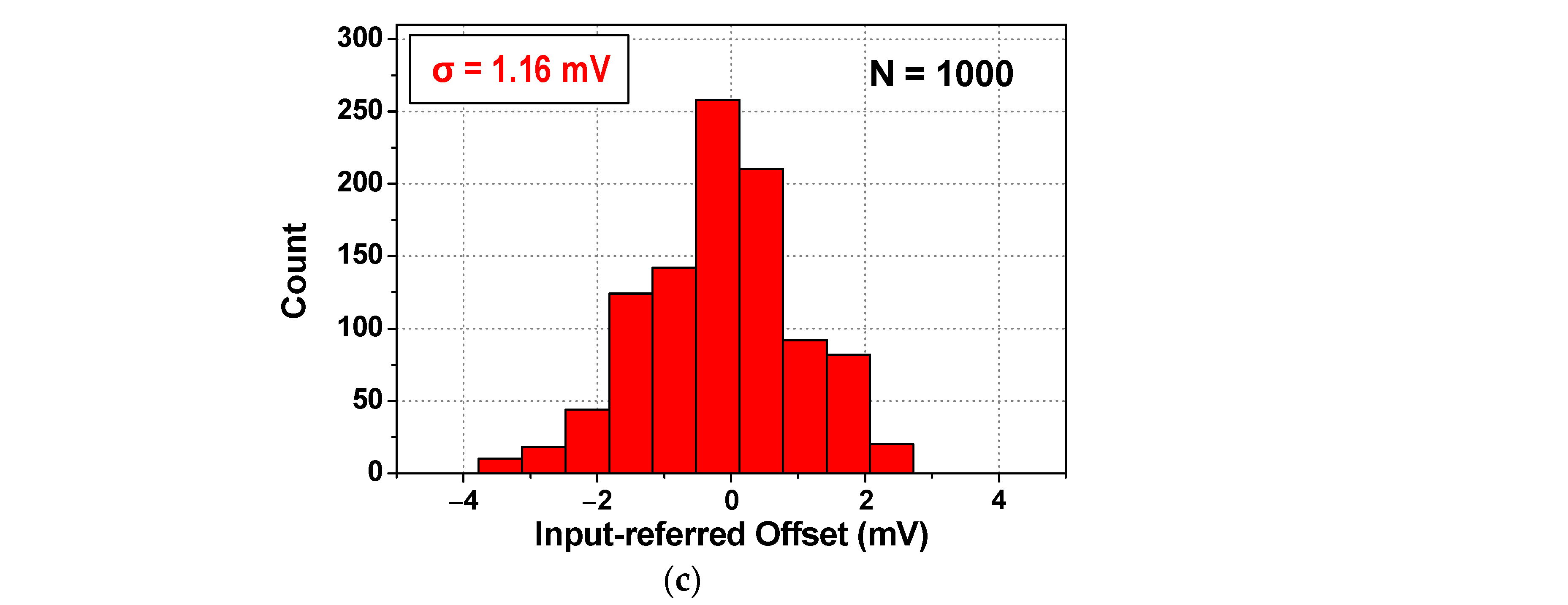
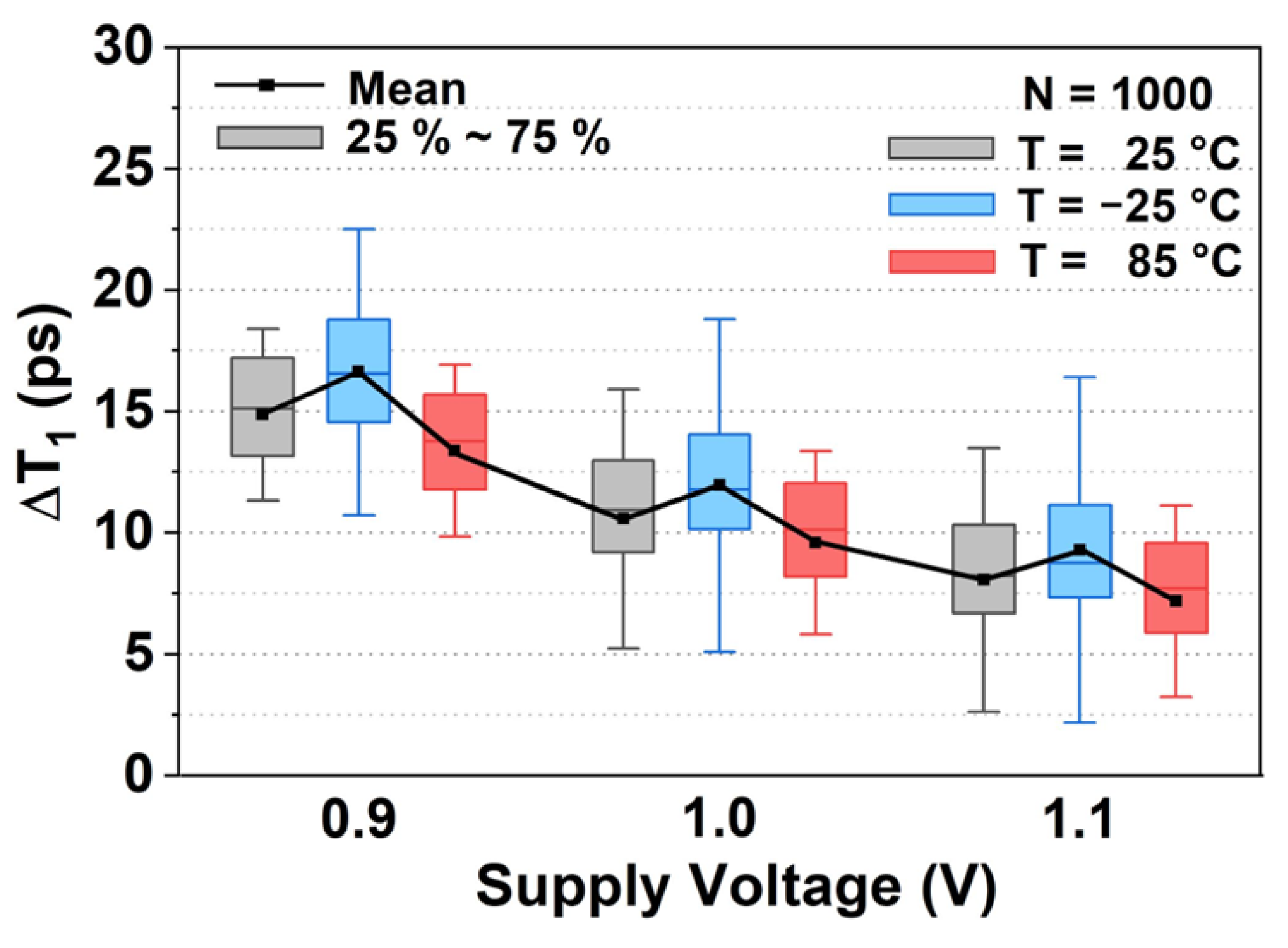
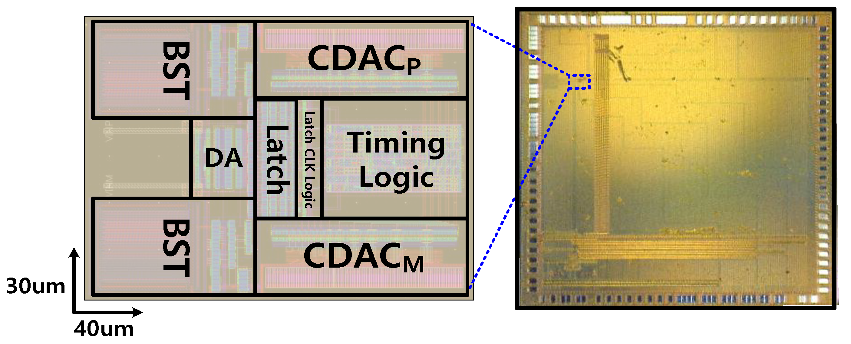
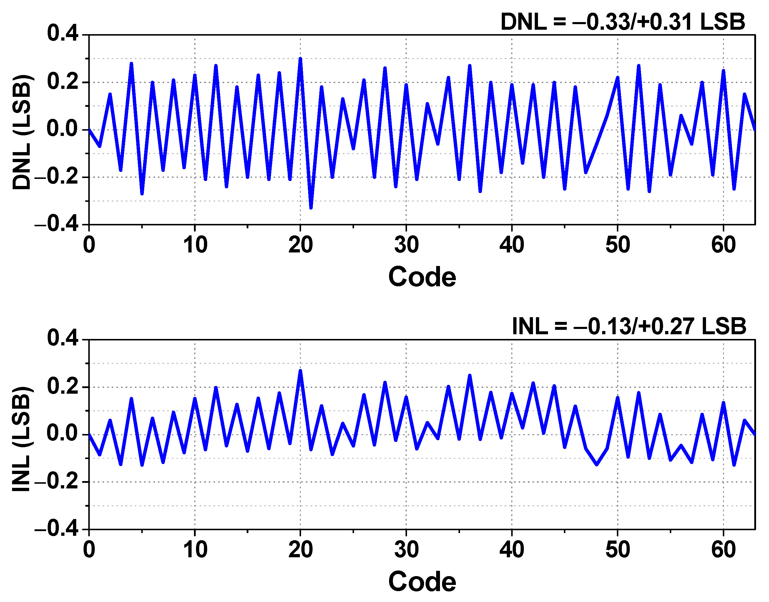
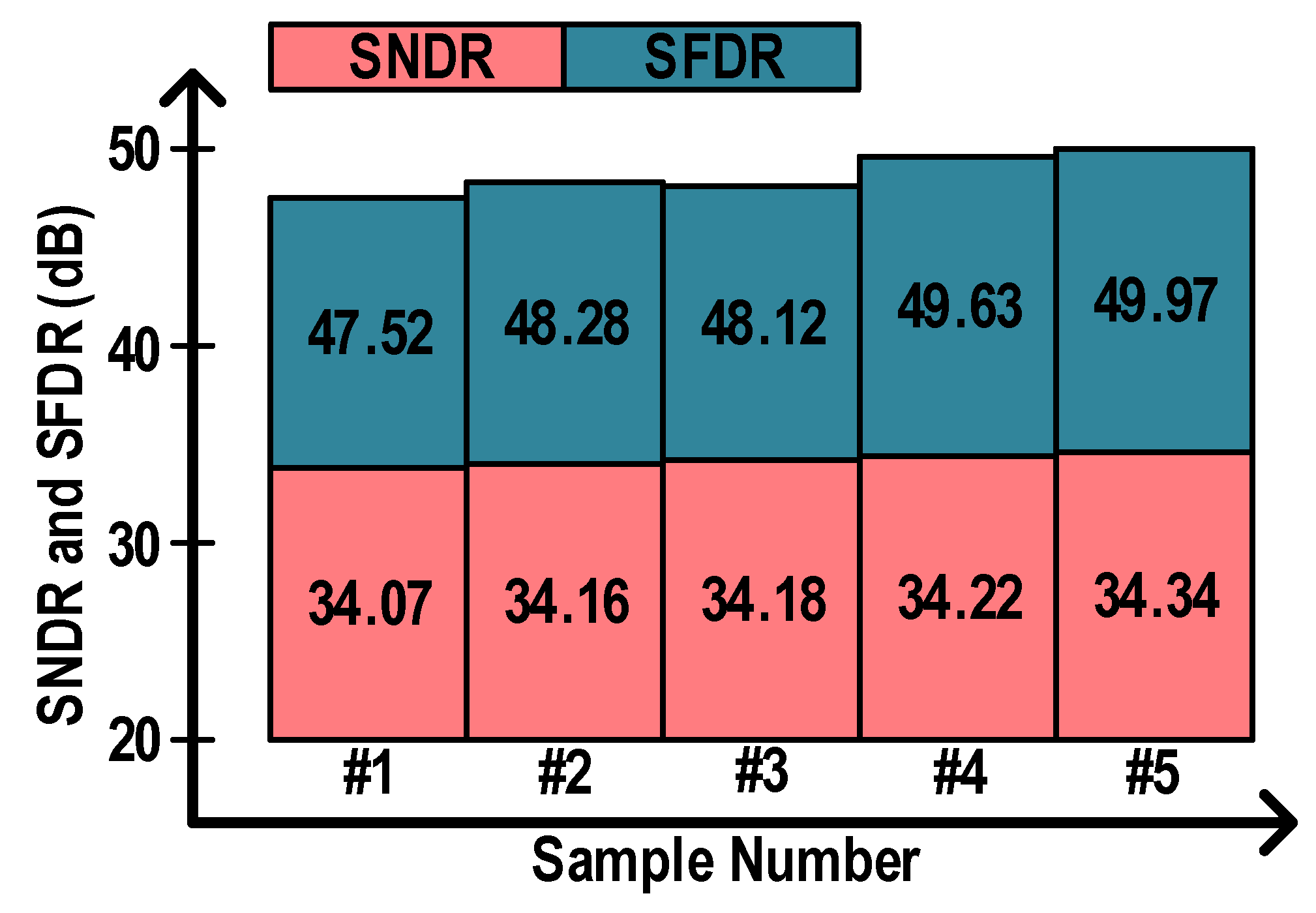
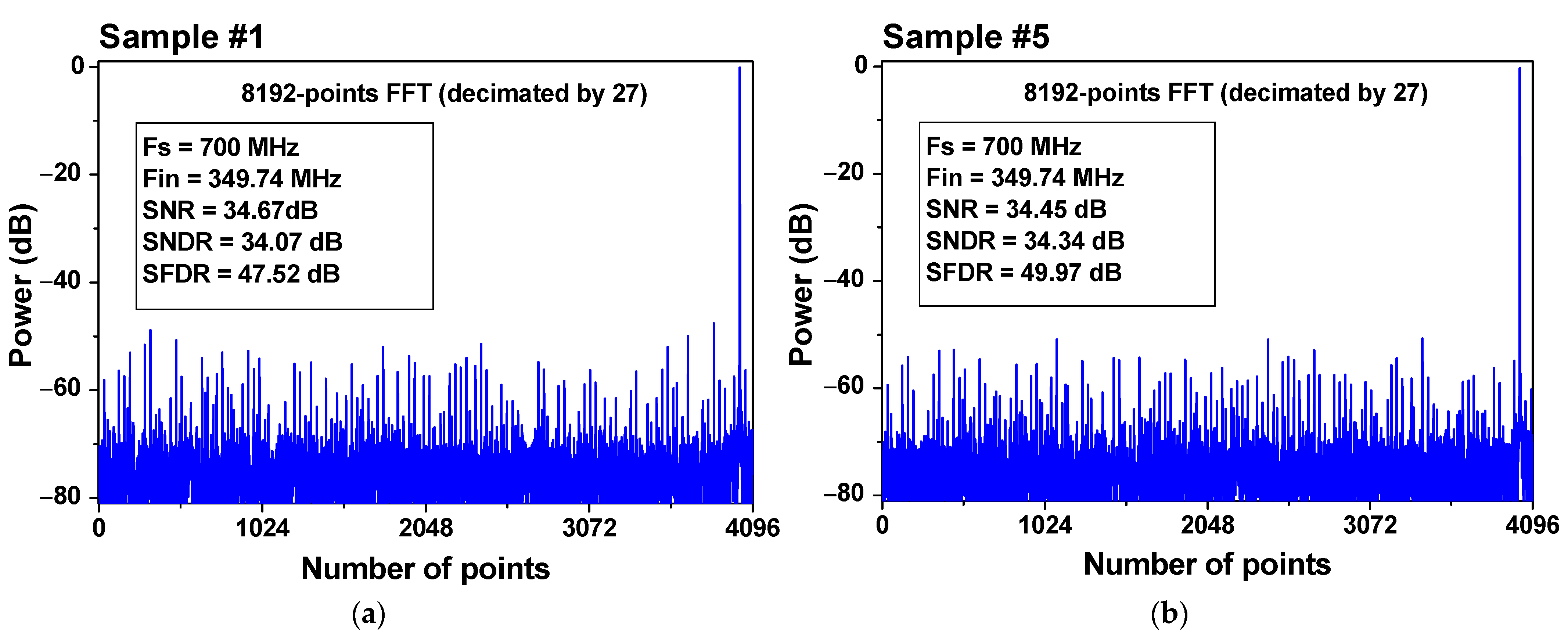
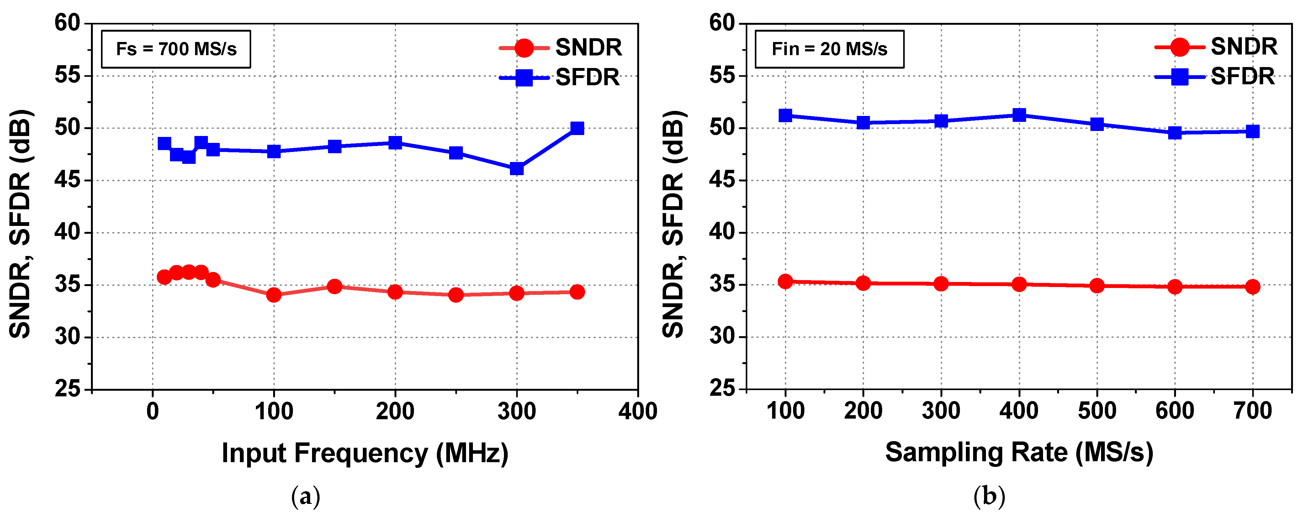
5. Measurement Results

A prototype 6-bit calibration-free P-LU SAR ADC was designed to have a 700 MS/s conversion rate in a 28 nm CMOS process. Figure 10 shows a die photograph. Since the LU SAR conversion is possible without a calibration engine by utilizing the ST-DA and the inverter-inserted comparator, the proposed ADC can be designed as compact as the conventional asynchronous SAR ADCs with enhanced conversion speed. As a result, the core area of the proposed P-LU SAR ADC including sampling network, DA, latches, clock generator, and CDAC was 30 μm × 40 μm.
The measured DNL and INL are shown in Figure 11. With the application of the ST-DA and the inverter-inserted comparators, the peak DNL and INL values were −0.33/+0.31 LSB and −0.13/+0.27 LSB, respectively.
The measured signal-to-noise and distortion ratio (SNDR) and spurious-free dynamic range (SFDR) results of five samples with a 349.74 MHz input at a 700 MS/s are shown in Figure 12. The SNDR and SFDR for the five samples were above 34 dB and 47 dB, respectively. Although the number of measurement samples was rather limited, these measurement results indirectly showed that the proposed ADC could achieve good performance without an offset calibration.
Figure 13 shows the fast Fourier transform (FFT) results of the minimum (Figure 13a: Sample #1) and maximum (Figure 13b: Sample #5) SNDR among the five samples shown in Figure 12. As shown in Figure 13a, the minimum SNDR and SFDR were 34.07 dB and 47.52 dB, respectively, and the effective number of bits (ENOB) was 5.36 bits even without comparator offset calibration.
The dynamic performances with various input frequencies and sampling rates are shown in Figure 14a,b, respectively. Below 200 MHz input frequency, the SFDR degraded due to a measurement environment issue, but the SNDR was very linear up to the Nyquist input frequency. Moreover, the SNDR was quite constant regardless of the sampling rate.
Figure 15 shows the measured SNDR and SFDR with various supply voltages. Even with ±10% supply variation, the ADC performance stayed constant in the condition of a 249.82 MHz input at 500 MS/s.
The prototype ADC operated under a 1 V supply and consumed 1.0 mW power at a 700 MS/s sampling rate. Figure 16 shows the power breakdown. For the gain of the ST-DA to reduce the input-referred offset mismatch and the high-speed design of the latch, the power consumption of the ST-DA, inverters, and six latches was the highest at 41%, followed by the CG block with 31%.
In Table 2, the performance of the proposed ADC is summarized and compared with those of recently reported 6–8 bits ADCs with sampling frequency and architecture similar to our design. The proposed ADC was designed with competitive conversion speed compared to the previously reported LU SAR ADCs. In addition, thanks to the P-LU SAR architecture with shared DA and an inverter-inserted comparator, the proposed ADC did not require offset calibration. In the LU SAR ADC, since the comparator does not reset until the SAR conversion is finished, the input kickback error accumulates in the CDAC every comparison cycle [18]. Therefore, as in [18], the LU SAR ADC should also consider the offset calibration for the input common change. On the other hand, in the proposed P-LU SAR ADC, since the six latches share one DA that repeats reset and trigger every comparison cycle, the proposed P-LU SAR ADC is very linear without an additional calibration circuit. As a result, the core area was designed to 0.002 mm2, which was the smallest among the compared ADCs as shown in Table 2. Therefore, the proposed P-LU SAR ADC can be used as compact single channel ADC for high-speed TI ADC. The achieved Walden figure-of-merit (FOM) was competitive at 34.6 fJ/conversion step.

6. Conclusions

A 6-bit 700 MS/s calibration-free P-LU SAR ADC was presented in a 28 nm CMOS process. The proposed inverter-inserted three-stage comparator with a shared DA removed the mismatches of the input transistors. Moreover, the mismatches of the latches were reduced by the gain of the DA. Therefore, this design relaxes the burden of calibration in LU SAR ADC, with competitive speed, and enables a compact area. At a 700 MS/s sampling rate, the prototype ADC consumed 1.0 mW under 1 V power supply, and the ENOB was 5.36 bits under Nyquist input. The proposed ADC achieved a Walden FOM of 34.6 fJ/conversion step, and only occupies a core area of 0.0012 mm2.

Author Contributions

Conceptualization, D.-R.O. and E.-J.A.; methodology, D.-R.O. and E.-J.A.; investigation, D.-R.O.; resources, D.-R.O. and E.-J.A.; writing—original draft preparation, E.-J.A.; writing—review and editing, D.-R.O. All authors have read and agreed to the published version of the manuscript.

Funding

This research received no external funding.

Conflicts of Interest

The authors declare no conflict of interest.

Abbreviations

SARSuccessive approximation register
ADCAnalog-to-digital converter
DADynamic amplifier
ST-DASelf-triggered DA
LULoop-unrolled
P-LUPseudo-loop-unrolled
CGClock generation
BTSBootstrapped
T/HTrack-and-hold
CDACCapacitive digital-to-analog converter
SNRSignal-to-noise ratio
SNDRSignal-to-noise distortion ratio
SFDRSpurious-free dynamic range
ENOBEffective number of bits
DNLDifferential non-linearity
INLIntegrated non-linearity
FoMFigure-of-merit

References

  1. Mishra, P.; Tan, A.; Helal, B.; Ho, C.R.; Loi, C.; Riani, J.; Sun, J.; Mistry, K.; Raviprakash, K.; Tse, L.; et al. A 112Gb/s ADC-DSP-Based PAM-4 Transceiver for Long-Reach Applications with >40 dB Channel Loss in 7 nm FinFET. In Proceedings of the IEEE International Solid-State Circuits Conference Digest of Technical Papers, San Francisco, CA, USA, 13–22 February 2021. [Google Scholar]
  2. Bailey, J.; Shakiba, H.; Nir, E.; Marderfeld, G.; Krotnev, P.; LaCroix, M.A.; Cassan, D. A 112Gb/s PAM-4 Low-Power 9-Tap Sliding-Block DFE in a 7 nm FinFET Wireline Receiver. In Proceedings of the IEEE International Solid-State Circuits Conference Digest of Technical Papers, San Francisco, CA, USA, 13–22 February 2021. [Google Scholar]
  3. Wang, D.; Wang, Z.; Xu, H.; Wang, J.; Zhao, Z.; Zhang, C.; Wang, Z.; Chen, H. A 56-Gbps PAM-4 Wireline Receiver with 4-Tap Direct DFE Employing Dynamic CML Comparators in 65 nm CMOS. IEEE Trans. Circuits Syst. I Regul. Pap. 2022, 69, 1027–1040. [Google Scholar] [CrossRef]
  4. Jiang, W.; Zhu, Y.; Chan, C.H.; Murmann, B.; Martins, R.P. A 7-bit 2GS/s Time-Interleaved SAR ADC with Timing Skew Calibration Based on Current Integrating Sampler. IEEE Trans. Circuits Syst. I Regul. Pap. 2021, 68, 557–568. [Google Scholar] [CrossRef]
  5. Ali, A.M.A.; Dinc, H.; Bhoraskar, P.; Bardsley, S.; Dillon, C.; Kumar, M.; McShea, M.; Bunch, R.; Prabhakar, J.; Puckett, S. A 12b 18GS/s RF Sampling ADC with an Integrated Wideband Track-and-Hold Amplifier and Background Calibration. In Proceedings of the IEEE International Solid-State Circuits Conference Digest of Technical Papers, San Francisco, CA, USA, 16–20 February 2020. [Google Scholar]
  6. Seo, M.J. A Single-Amplifier Dual-Residue Pipelined-SAR ADC. Electronics 2021, 10, 421. [Google Scholar] [CrossRef]
  7. Hong, H.-K.; Kang, H.-W.; Sung, B.; Lee, C.-H.; Choi, M.; Park, H.-J.; Ryu, S.-T. An 8.6 ENOB 900 MS/s Time-Interleaved 2b/cycle SAR ADC with a 1b/cycle Reconfiguration for Resolution Enhancement. In Proceedings of the IEEE International Solid-State Circuits Conference Digest of Technical Papers, San Francisco, CA, USA, 17–21 February 2013; pp. 470–471. [Google Scholar]
  8. Seo, M.-J.; Kim, Y.-D.; Chung, J.-H.; Ryu, S.-T. A 40 nm CMOS 12b 200 MS/s Single-amplifier Dual-residue Pipelined-SAR ADC. In Proceedings of the IEEE Symposium on VLSI Circuits Digest of Technical Papers, Kyoto, Japan, 9–14 June 2019. [Google Scholar]
  9. Nam, J.; Hassanpourghadi, M.; Zhang, A.; Chen, M.S.-W. A 12-Bit 1.6, 3.2, and 6.4 GS/s 4-b/Cycle Time-Interleaved SAR ADC with Dual Reference Shifting and Interpolation. IEEE J. Solid State Circuits 2018, 53, 1765–1779. [Google Scholar] [CrossRef]
  10. Seo, M.J.; Jin, D.H.; Kim, Y.D.; Kim, J.P.; Ryu, S.T. A Single-Supply CDAC-Based Buffer-Embedding SAR ADC with Skip-Reset Scheme Having Inherent Chopping Capability. IEEE J. Solid State Circuits 2020, 55, 2660–2669. [Google Scholar] [CrossRef]
  11. Luu, D.; Kull, L.; Toifl, T.; Menolfi, C.; Braendli, M.; Francese, P.A.; Morf, T.; Kossel, M.; Yueksel, H.; Cevrero, A.; et al. A 12-bit 300-MS/s SAR ADC with Inverter-Based Preamplifier and Common-Mode-Regulation DAC in 14-nm CMOS FinFET. IEEE J. Solid State Circuits 2018, 53, 3268–3279. [Google Scholar] [CrossRef]
  12. Wang, D.; Zhu, X.; Guo, X.; Luan, J.; Zhou, L.; Wu, D.; Liu, H.; Wu, J.; Liu, X. A 2.6 GS/s 8-Bit Time-Interleaved SAR ADC in 55 nm CMOS Technology. Electronics 2019, 8, 305. [Google Scholar] [CrossRef] [Green Version]
  13. Li, J.; Guo, X.; Luan, J.; Wu, D.; Zhou, L.; Wu, N.; Huang, Y.; Jia, H.; Zheng, X.; Wu, J.; et al. A 1 GS/s 12-Bit Pipelined/SAR Hybrid ADC in 40 nm CMOS Technology. Electronics 2020, 9, 375. [Google Scholar] [CrossRef] [Green Version]
  14. Chen, S.M.; Brodersen, R.W. A 6b 600 MS/s 5.3 mW Asynchronous ADC in 0.13 μm CMOS. In Proceedings of the IEEE International Solid-State Circuits Conference Digest of Technical Papers, San Francisco, CA, USA, 6–9 February 2006. [Google Scholar]
  15. Jiang, T.; Liu, W.; Zhong, F.Y.; Zhong, C.; Hu, K.; Chiang, P.Y. A Single-Channel, 1.25-GS/s, 6-bit, 6.08-mW Asynchronous Successive-Approximation ADC with Improved Feedback Delay in 40-nm CMOS. IEEE J. Solid-State Circuits 2012, 47, 2444–2453. [Google Scholar] [CrossRef]
  16. Chen, L.; Ragab, K.; Tang, X.; Song, J.; Sanyal, A.; Sun, N. A 0.95-mW 6-b 700-MS/s Single-Channel Loop-Unrolled SAR ADC in 40-nm CMOS. IEEE Trans. Circuits Syst. II Express Briefs 2017, 64, 244–248. [Google Scholar] [CrossRef]
  17. Chen, C.; Sun, J.; Wang, C.; Liu, W. A 10-b 500 MS/s Partially Loop-Unrolled SAR ADC with a Comparator Offset Calibration Technique. In Proceedings of the IEEE International Symposium on Circuits and Systems, Daegu, Korea, 22–28 May 2021. [Google Scholar]
  18. Akkaya, A.; Celik, F.; Leblebici, Y. An 8-Bit 800 MS/s Loop-Unrolled SAR ADC with Common-Mode Adaptive Background Offset Calibration in 28 nm FDSOI. IEEE Trans. Circuits Syst. I Regul. Pap. 2021, 68, 2766–2774. [Google Scholar] [CrossRef]
  19. Ragap, K.; Sun, N. A 1.4 mW 8b 350 MS/s Loop-Unrolled SAR ADC with Background Offset Calibration in 40 nm CMOS. In Proceedings of the IEEE European Solid-State Circuits Conference, Lausanne, Switzerland, 12–15 September 2016. [Google Scholar]
  20. Kull, L.; Luu, D.; Menolfi, C.; Brändli, M.; Francese, P.A.; Morf, T.; Kossel, M.; Cevrero, A.; Ozkaya, I.; Toifl, T. A 24–72-GS/s 8-b Time-Interleaved SAR ADC with 2.0–3.3-pJ/Conversion and >30 dB SNDR at Nyquist in 14-nm CMOS FinFET. IEEE J. Solid-State Circuits 2018, 53, 3508–3516. [Google Scholar] [CrossRef]
  21. Chung, Y.-H.; Rih, W.-S.; Chang, C.-W. A 6-bit 1.3-GS/s Ping-Pong Domino-SAR ADC in 55-nm CMOS. IEEE Trans. Circuits Syst. II Express Briefs 2018, 65, 999–1003. [Google Scholar] [CrossRef]
  22. Oh, D.R.; Moon, K.J.; Lim, W.M.; Kim, Y.D.; An, E.J.; Ryu, S.T. An 8-Bit 1-GS/s Asynchronous Loop-Unrolled SAR-Flash ADC with Complementary Dynamic Amplifiers in 28-nm CMOS. IEEE J. Solid-State Circuits 2021, 56, 1216–1226. [Google Scholar] [CrossRef]
  23. Schinkel, D.; Mensink, E.; Klumperink, E.; Tuijl, E.V.; Nauta, B. A Double-Tail Latch-Type Voltage Sense Amplifier with 18 ps Setup-Hold Time. In Proceedings of the IEEE International Solid-State Circuits Conference Digest of Technical Papers, San Francisco, CA, USA, 11–15 February 2007. [Google Scholar]
  24. Kim, W.; Hong, H.K.; Roh, Y.J.; Kang, H.W.; Hwang, S.I.; Jo, D.S.; Chang, D.J.; Seo, M.J.; Ryu, S.T. A 0.6 V 12b 10 MS/s Low-Noise Asynchronous SAR-Assisted Time-Interleaved SAR (SATI-SAR) ADC. IEEE J. Solid-State Circuits 2016, 51, 1826–1839. [Google Scholar] [CrossRef]
  25. Li, D.; Liu, J.; Zhuang, H.; Zhu, Z.; Yang, Y.; Sun, N. A 7b 2.6 mW 900 MS/s Nonbinary 2-Then-3b/cycle SAR ADC with Background Offset Calibration. In Proceedings of the IEEE Custom Integrated Circuits Conference (CICC), Austin, TX, USA, 14–17 April 2019. [Google Scholar]
  26. Chan, C.H.; Zhu, Y.; Sin, S.W.; Ben, S.P.U.; Martins, R.P. A 6b 5 GS/s 4 Interleaved 3b/Cycle SAR ADC. IEEE J. Solid-State Circuits 2016, 51, 365–377. [Google Scholar]
  27. Kiene, G.; Catania, A.; Overwater, R.; Bruschi, P.; Charbon, E.; Babaie, M.; Sebastiano, F. A 1 GS/s 6-to-8b 0.5 mW/Qubit Cryo-CMOS SAR ADC for Quantum Computing in 40 nm CMOS. In Proceedings of the IEEE International Solid-State Circuits Conference Digest of Technical Papers, San Francisco, CA, USA, 13–22 February 2021. [Google Scholar]
Figure 1. Conceptual block and timing diagram of conventional LU SAR ADC [15,16,17,18,19,20].
Electronics 11 01707 g001
Figure 2. Conceptual block and timing diagram of proposed calibration-free P-LU SAR ADC.
Electronics 11 01707 g002
Figure 3. Comparison of the main clock paths of (a) the LU SAR ADC and (b) the proposed P-LU SAR ADC.
Electronics 11 01707 g003
Figure 4. Inverter-inserted three-stage comparator. (a) Circuit and (b) timing diagrams.
Electronics 11 01707 g004
Figure 5. Monte Carlo simulation results of input-referred offset mismatch. (a) Strong-arm latch, (b) DA + latch, and (c) inverter-inserted comparator (this work).
Electronics 11 01707 g005aElectronics 11 01707 g005b
Figure 6. Logic for the CG block in P-LU SAR ADC and the timing diagram.
Electronics 11 01707 g006
Figure 7. Mean and standard deviation of ΔT1 ( = t Logic 1 + t DA , rst   t Latch ) under supply voltage and temperature variation.
Electronics 11 01707 g007
Figure 8. Latch EN GEN with domino logic using tri-state inverters. (a) Block and (b) timing diagrams.
Electronics 11 01707 g008
Figure 9. Mean and standard deviation of ΔT2 (rising edge of Φ DA minus the rising edge of Φ EN ) under supply voltage and temperature variation.
Electronics 11 01707 g009
Figure 10. Die photograph.
Electronics 11 01707 g010
Figure 11. Measured DNL and INL.
Electronics 11 01707 g011
Figure 12. Measured SNDR and SFDR from five different samples near Nyquist input at 700 MS/s.
Electronics 11 01707 g012
Figure 13. Measured FFT spectrums with a 349.74 MHz input at a 700 MS/s sampling rate. (a) Sample #1. (b) Sample #5.
Electronics 11 01707 g013
Figure 14. Measured SNDR and SFDR with various (a) input frequencies at 700 MS/s, (b) sampling rates with a 20 MHz input.
Electronics 11 01707 g014
Figure 15. Measured SNDR and SFDR with various supply voltages within ± 10%.
Electronics 11 01707 g015
Figure 16. Power breakdown.
Electronics 11 01707 g016
Table 1. Comparison for SAR ADC architectures.
N-bitAsync. SAR [14]LU SAR [15,16,17]
(Boreground cal.)
LU SAR [18,19,20]
(Background cal.)
LU SAR + SAR [21]
(Redundancy bit)
P-LU SAR
(This Work)
# of comparators1NN + 1NOne DA + N
# of input gates1NN + 1N1
Conversion cycleNNN + 1N + 1N
Offset calibrationNot neededNeededNeededNot neededNot needed
Comparator resetNeededNot neededNot neededPartially NeededHidden
DAC switching logicNeededNot neededNot neededNot neededNot needed
Table 2. Performance comparison.
This WorkESSCIRC16
Ragab
[19]
TCAS17
Chen
[16]
TCAS18
Chung
[21]
TCAS21
Akkaya
[18]
CICC19
Li
[25]
JSSC21
Oh
[22]
JSSC16
Chan
[26]
ISSCC21
Kiene
[27]
ArchitectureP-LU SARLU SARLU SARLU SAR + SARLU SAR2–3b/cycleSAR-FlashTI 3b/cycleTI LU SAR
# of channels111111142
Technology (nm)2840405528(FDSOI)40286540
Resolution (bit)686687866
FS (GS/s)0.70.350.71.30.80.9150.9
Area (mm2)0.00120.024 10.0040.030.00370.0140.00560.090.045
Supply (V)1.01.11.21.21.01.11.11.01.1
DNLMAX (LSB)0.330.90.90.780.740.50.591.40.5 1
INLMAX (LSB)0.270.90.60.850.650.80.820.950.5 1
CIN (fF)3224930.4326425.2643163.5
SNDR@Nyq. (dB)34.043.734.830.542.539.745.530.733.4
SFDR@Nyq. (dB)47.559.547.836.350.754.859.443.148.4
Power (mW)1.01.370.953.522.62.555.50.7
Walden FOM 2
(fJ/conv.-step)
34.631.330.09922.836.616.63920
Offset
Calibration
Not neededBackgroundForegroundNot neededBackgroundBackgroundForegroundForegroundForeground
1 Estimated value. 2 Walden FoM = Power/(2ENOB × Sampling frequency).
Publisher’s Note: MDPI stays neutral with regard to jurisdictional claims in published maps and institutional affiliations.

