1. Introduction
In order to create a green communication infrastructure focused on the minimization of the energy consumption, the power amplifier (PA) has a primary role within the transceiver. This translates to a need of developing high frequency, wideband, and energy efficient PAs, that allow covering as wide a portion of the frequency spectrum as possible, especially towards the millimeter waves, answering the high data rates and energy performance requirements simultaneously.
The enabling technologies for mm-wave transmitters are those that allow achieving sufficient power levels at the integrated circuit level, which is far more compact, flexible, energy and size efficient than combining the power of several chips. Two compound technologies are today available for the realization of monolithic microwave integrated circuit (MMIC) PAs with reasonable power, gallium arsenide pseudomorphic high electron mobility transistors (GaAs pHEMTS) and, more recently, gallium nitride (GaN) HEMTs. GaAs is more mature and less expensive, but GaN offers power densities three to four times higher, thanks to its higher operating voltage, allowing for the realization of larger power on-chip and relaxing the off-chip bulky power combiners. GaN is offered both grown on a silicon carbide (SiC) substrate—expensive but more mature—and, recently, on a silicon (Si) substrate, which is more challenging in terms of performance, but allows a higher level of integration with the rest of the Si-based embedded systems.
To satisfy the need for very high data rates, the adoption of increasingly high carrier frequencies and spectrally efficient modulating signals is common to ground and satellite applications. This poses more demanding constraints on the PA, that must operate efficiently not only at peak output power levels, but also at lower output powers, in the so-called output back off (OBO) region, which depends, in turn, on the peak-to-average power ratio (PAPR) of the adopted signal.
Combined-class AB PAs have demonstrated the capability to provide the required power levels with high saturated efficiency levels, up to the Ka band [
1,
2], but they clearly suffer a marked drop in average efficiency when operated with non-constant envelope modulations. High efficiency, in OBO, can be achieved either by applying specific circuit design strategies or system-level solutions. At the MMIC level, some of the most adopted PA architectures are based on the load modulation concept [
3]. To this category belong the Doherty PA (DPA) [
4], the outphasing PA [
5,
6] and the Load Modulated Balanced Amplifier (LMBA) [
7,
8]. Among the others, at communication frequencies (sub 6 GHz), the DPA architecture is, today, the most popular solution, being an all-RF and yet somehow simple architecture. Its adoption as a viable alternative to corporate PAs—also for applications at microwave and mm-wave frequencies—is, on the other hand, a very hot topic of great interest for the research community from the view of its exploitation in future networks.
This paper discusses different power combination approaches for the design of watt-level integrated DPAs in the K bands (between 18 GHz and 42 GHz) based on compound semiconductor technologies, and is organized as follows. In
Section 2, the different power combination strategies available are discussed, highlighting advantages and disadvantages, in both GaAs and GaN technologies. Examples of MMIC DPAs recently published in the literature are presented to illustrate the different possibilities. A simplified simulated case study is developed in
Section 3 resorting to an approximate linear analysis, not requiring a full non-linear model of the employed active devices. The design of a DPA combiner, operating at 22 GHz and targeting backhaul applications, is proposed for two sample technologies, GaAs and GaN, and then for the several power combination strategies in GaN, which is the only examined device that allows achieving the required power level directly on chip. The impacts on bandwidth and achievable performance of the various choices are assessed, thus performing a novel systematic comparison at the simulation level of the three main strategies to combine power in an MMIC DPA. The impact of the output parasitic effects of the transistors on the presented analysis is also briefly discussed in the context of one of the analyzed topologies. Finally, conclusions are drawn in
Section 4.
2. Power Levels and On-Chip Combination
The power level required from the RF transmitter is a fundamental characteristic of the communication system, deeply influencing the PA design in terms of technology and architecture employed. It differs significantly according to the specific application, spanning from hundreds of watts, for huge base stations at low communication frequencies (sub 6 GHz), down to fractions of watts in the upper end of the mm-wave spectrum (up to 110 GHz).
In K bands (between 18 GHz and 42 GHz), both for ground (mobile backhauling and, more recently, 5G-FR2) and for satellite transmitters, the typical power levels are in the 5–50 W range. More specifically, mobile backhauling applications require power levels on the order of 5–10 W [
9], while analog phased arrays exploit 5G-FR2 New radio adopt similar power levels in the frequency band around 28 GHz and less in the 37–40 GHz one. For satellite applications, the overall power required is higher, reaching 50–60 W, but, in the view of replacing travelling wave tube amplifiers (TWTAs) with solid state PAs (SSPAs) [
10,
11], 5–10 W requirements, at the chip level, are appearing.
Technologies with sufficient power density to achieve these output power targets at the chip level are based on compound semiconductors, namely GaAs and GaN, with gate lengths between 100 nm and 150 nm. However, despite the high power density of compound semiconductors, several transistors have to be combined to achieve watt-level output power at the MMIC level with mm-waves.
Two GaAs watt-level DPAs for K-band applications, such as point-to-point radio links, are presented in [
12,
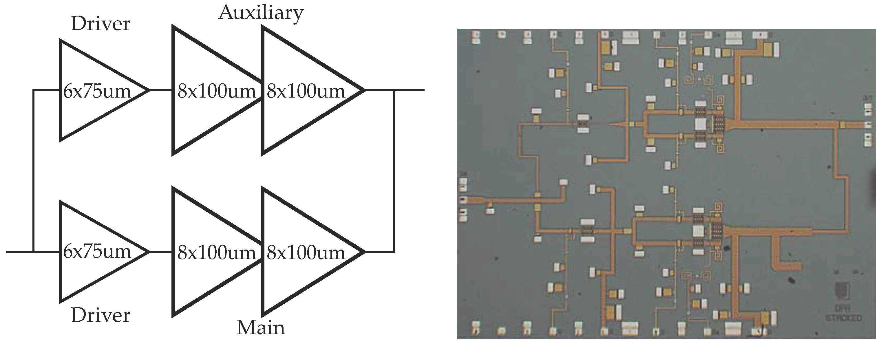
13]. The block diagram and chip photographs are reported in
Figure 1. Both DPAs are two-stage architectures embedding the driver stage within each branch of the DPA, and result in chip areas of 4.3 mm
and 3.8 mm
, respectively. They differ strongly in the strategy adopted to realize the output combiner, and have, therefore, similar maximum power and gain but different bandwidths, with [
13] resulting in a wider bandwidth than [
12]. With an overall active periphery around 2 mm (i.e., 1 mm per device for a symmetrical DPA with a main and an auxiliary of the same size), a saturated power level close to 1W is achieved, which is the maximum achievable without an on-chip power combination. To reach the power levels required by the application, off-chip power combination is mandatory.
Other recent examples available in the literature confirm that the power achievable with this technology for the design of a MMIC DPA, either based on single devices for their main and auxiliary stages [
14,
15] or adopting some on-chip power combination [
16], cannot exceed the watt limit. This is also confirmed in
Table 1, which reports the performance of state-of-the-art MMIC DPAs, implemented in different technologies, operating in the K and Ka bands.
In [
24], a preliminary demonstration of an on-chip power combination at the DPA level is provided by comparing the CW performance of the DPA in [
12] with that of a combined PA based on two identical Doherty cells. At a single frequency, the combined DPA proves to achieve comparable gain and PAE while doubling the output power, thus, achieving around 2 W from a single chip. This comes at the price of a more complex architecture, especially in terms of the routing of the bias lines and of increased chip area. Additionally, the analysis is not extended to the behavior over the whole bandwidth.
Being the maximum active periphery, i.e., one that allows for sufficient gain and limited phase misalignment among transistor fingers and similar between the GaAs and GaN processes (roughly 1 mm per device, i.e., 2 mm overall for a symmetric 6-dB DPA), the wide bandgap and consequently higher breakdown voltage of GaN allows achieving power densities four times higher than in GaAs (around 2 W/mm instead of 0.5 W/mm) permitting to reach with this technology output powers of up to 4W from a single-chip DPA without any power combination [
21,
22,
23]. Considering as a reasonable on-chip power combination one that doubles the active periphery, single-chip DPAs achieving up to 8 W can be expected. The achievable power lowers somewhat when wideband operation is desired, since maintaining the load modulation over wide frequency ranges often calls for sub-optimal loading conditions at saturation.
Several power combination strategies for MMIC DPAs have been tested in [
25,
26,
27], adopting the D01GH GaN-Si HEMT process provided by OMMIC. The considered possibilities for combining power on-chip, which cover most of the solutions typically adopted except for the distributed PA and its derivatives [
28], are the following: combination of devices in parallel (current summing), stacking of devices (voltage summing), combination of PAs in parallel (current summing). The DPAs target satellite applications in the 17.3–20.3 GHz band.
A DPA cell based on the largest transistor available for the selected process is presented in [
26]. It has been realized with the aim of testing the effectiveness of an on-chip power combination at the DPA level. In fact, the cell is matched to 100
at the output, allowing for the direct combination of two identical DPA cells in parallel on a standard 50
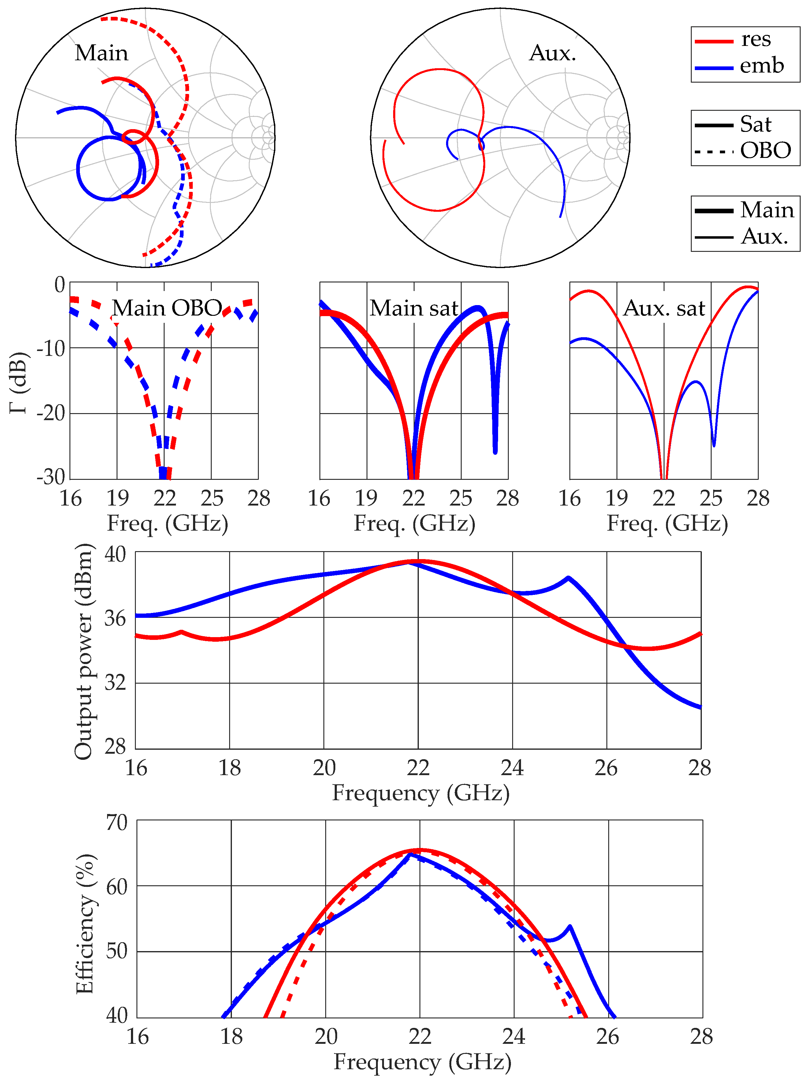
output impedance to achieve power levels on the order of 5–6 W. The DPA cell adopts a combiner based on the embedding of the output capacitance of the transistors, for wideband operation and featuring a post-matching network from the common node impedance to the output impedance. The layout of the latter has been devised to allow for the connection of two identical DPA cells in parallel without any additional circuit element. Similarly, the gate bias and drain supply lines are all routed to the same side, envisaging the DC routing of the final combined DPA. Analogously to the DPAs of
Figure 1, drivers are included in each of the DPA branches, which is essential to achieve sufficient gain while maximizing the power-added efficiency (PAE). The output power of the single DPA cell resulted in excess of 34 dBm in the whole band, with an associated gain around 12 dB, and an efficiency higher than 25% and 20%, at saturation and 6 dB OBO, respectively. The combined DPA was then designed, manufactured and is currently under characterization. Preliminary results are presented in [
25], where it is referred to as MMIC2. As shown in
Figure 2, this is a three-stage architecture, where an additional driver stage is inserted at the input, in front of the two-parallel combined DPA cells. This was necessary since the application required a power gain higher than 20 dB. This DPA, whose chip area is 30 mm
, is expected to deliver around 37–38 dBm saturated output power over the whole operating band (17.3–20.3 GHz), which is compatible with the application requirement.
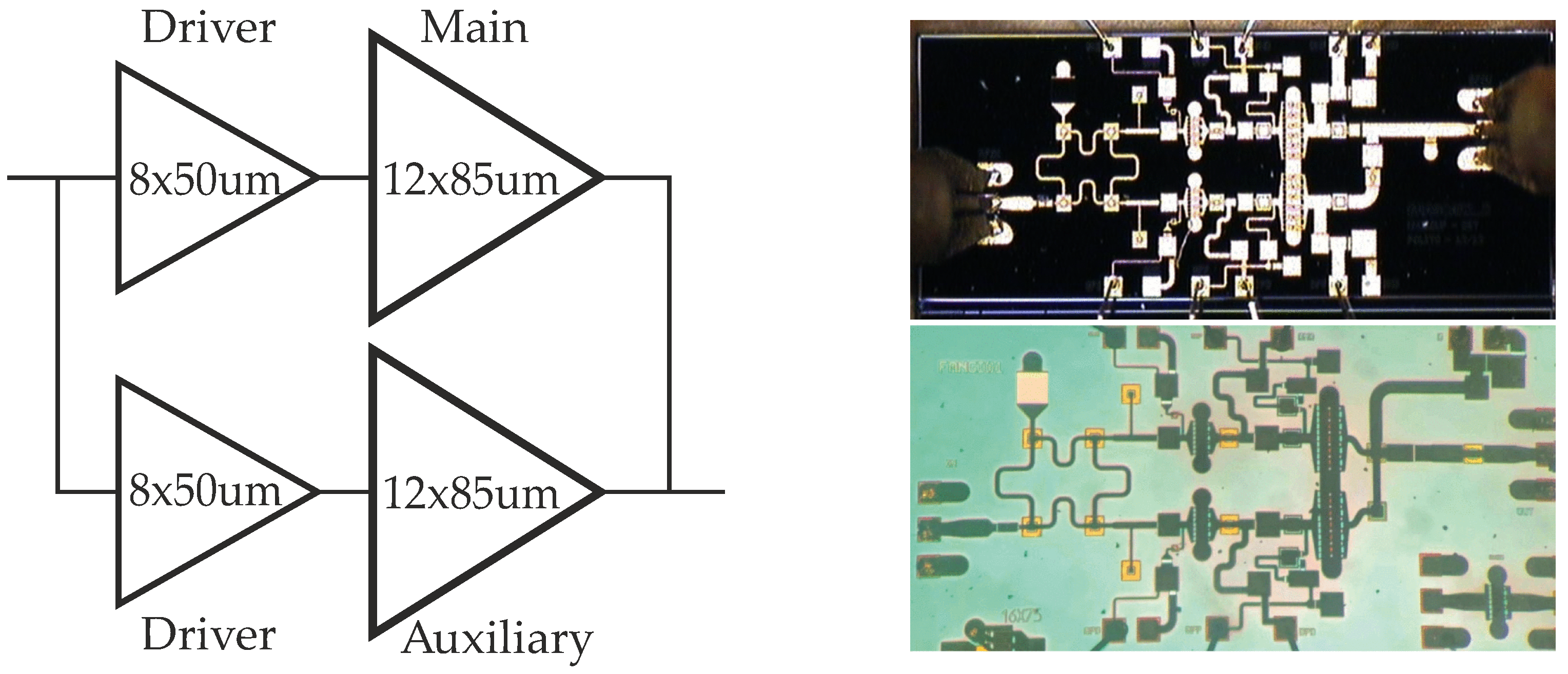
The device-level power combination is also explored in [
25], with the same technology and performance target, with MMIC1. It is a single DPA with main and auxiliary branches composed of two parallel-combined devices in the final stage. Ideally, when
N identical devices having operating current
and voltage
, optimum load
, power gain
G (expressed in linear units) are combined in parallel, the resulting structure can be represented as a “macro-device” with operating current
, supply voltage
, optimum load
and gain
G. In fact, the number of driver stages of MMIC1 is analogous to MMIC2, despite their periphery is different, as highlighted by the respective block diagrams in
Figure 2. The output section of the DPA consists of the compensation of the output parasitic effects of the transistors, performed by the structure physically connecting them and by a stub terminated by an RF-short circuit, which is also used to provide the drain supply to all the transistors in the final stage, and the TL-based combiner. The latter is composed of a low-impedance quarter-wavelength impedance inverter on the main and two quarter-wavelength TL sections on the auxiliary, designed to maximize the bandwidth and to adjust the back-off output impedance. The combiner also provides impedance transformation to 50
at the output. The performance expected from MMIC1 is analogous to MMIC2 in terms of gain and power, since the number of stages and the total final stage periphery is the same, whereas the efficiency is slightly higher at saturation and lower at OBO. This solution is convenient in terms of size, resulting in a chip area of 20 mm
, but allows a less accurate control of the load modulation of each transistor, possibly resulting in unbalances between each combined transistor pair that may cause different stress and performance.
A promising alternative to the classical parallel combination of devices (current summing) is represented by stacking, which can be seen as a series combination (voltage summing), since the transistors are stacked one on top of the other, increasing the drain supply voltage, the output impedance and gain with respect to the corresponding current summing combination. This is achieved at the expense of a more complex design and optimization phase, due to the higher integration level and to a lesser robustness in terms of stability. A standard N-stage stacked cell employs a common source (CS) device loaded by quasi-common gates (CG). Theoretically, when N identical devices, having operating current and voltage , optimum load , and power gain G (expressed in linear units), are adopted to realize an N-stage stacked cell, it has the operating current , supply voltage , optimum load , and gain . Therefore, this topology not only combines power, but also boosts gain and increases the optimum load impedance, which is typically beneficial at high frequency, where the gain of the individual transistor is limited and the optimum load is significantly lower than .
The stacked power combination has also been explored, in the same GaN-Si technology adopted for the above-mentioned MMICs, to realize a 5–6 W DPA. A two-stage stacked cell was developed first, testing different layouts and inter-stage matching structures, and characterized as stand-alone in a load-pull environment [
29,
30]. The preliminary results on the DPA based on the best performing cell, which is shown in
Figure 3, are presented in [
27]. The combiner topology adopted is analogous to that of MMIC1, despite having different impedance levels. The expected saturated output power is comparable to that of the other two architectures featuring the same overall periphery, i.e., around 38 dBm. The small-signal power gain of this DPA is expected to be in excess of 20 dB over its whole operating band (17.3–20.3 GHz), which is almost comparable to the gain of MMIC1 and MMIC2, which, however, have one extra driver stage at the input. This proves the effectiveness of the stacking in enhancing the gain while combining the power with a very compact layout [
31].
The on-chip power combination possibilities considered in this work are summarized in
Table 2, where the impedance transformation occurring in a 6dB DPA, whose main and auxiliary have the same active periphery, is also reported. The adopted notation refers to
as the optimum load of the individual transistor,
as the output impedance, and the transformation ratio,
r, of the DPA is defined as the ratio between output impedance of the DPA and the load to be synthesized at the current generator plane of the main and auxiliary branches when modeled by an equivalent current source. Therefore, considering that summing currents halves the impedance level while summing voltages doubles it, the optimum load and the output impedance are scaled accordingly in the various cases. Note that another possibility to combine DPAs in parallel exists that has not been considered here, i.e., adopting an in-phase (e.g., Wilkinson) or in-quadrature (e.g., Lange, broadside coupler) power combiner at the output, complemented with the appropriate power divider at the input to ensure the correct phase relation of the signals. This would allow designing each DPA cell on
rather than
, halving the impedance transformation ratio, but would introduce further losses that negatively impact efficiency. Whether this solution is more or less favorable compared to the other one depends on the constraints of the specific design.
3. Bandwidth Estimation
While the overall active periphery required in the final stage of the DPA can be approximately defined independently of the choice of the combiner topology, any consideration, however approximate, on the achievable bandwidth is closely related to the topological choices. Bandwidth, together with linearity, is a crucial aspect in determining the success of integrated PAs in a specific application, given the current trend leading standards towards wider frequency bands and increasing PAPR, and, therefore, deserves specific attention.
The object of this section is to compare the different active device technologies and power combination strategies mentioned in
Section 2, adopting a simple and fast estimation method. Therefore, a combiner topology is chosen that is general enough to be suitable to any of the cases to be analyzed. On the other side, it is not guaranteed that this is necessarily the most convenient topology.
The Doherty combiner adopted for the following analysis is shown in
Figure 4. It consists of a transmission line (TL) section of length
, where
at the design frequency
and characteristic impedance
, on the main, and two TL sections on the auxiliary (
and
, both
at
). If a design imposing exact load modulation (from
at 6dB OBO to
at saturation) at
is carried out, the common node impedance
is a degree of freedom. This allows, if desired, designing a Doherty combiner that is also performing impedance matching on the desired PA output impedance, typically 50
. If a different choice is made—which requires additional post-matching—this introduces a further frequency dependence that has an effect on the bandwidth. While at lower frequencies, and especially for hybrid implementations, the losses and circuit dimensions are such to allow for a post-matching structure complex enough not to be the limiting factor for bandwidth, at K bands and above, matching networks with more than a couple of stages are typically unfeasible. Therefore, post-matching topological strategies should be considered and compared in determining the overall bandwidth. In this case, in order to provide some simple guidelines and limit the number of analyzed cases,
is adopted. The design formulas for the combiner are:
which implies that one between
and
is a free parameter. While the choice of
has already been discussed,
,
are selected to maximize the bandwidth, with the additional constraint that all characteristic impedances correspond to feasible microstrip lines (and therefore, roughly,
).
To estimate the bandwidth of the DPA combiner we employ the method presented in [
32], based on a linear analysis in which the active devices are represented by current sources
,
, whose value depends on the input voltage as shown in
Figure 4. The combiner, including the load, is represented by a two-port
matrix, obtained by appropriate conversion formulas from the corresponding
matrix, which is easily obtained as the product of the individual
matrices of the circuit elements. The main and auxiliary devices are assumed to have drain supply voltage
, and maximum current
and
, respectively, where
when the devices have the same size. The fundamental currents are
where
,
are the fundamental Fourier coefficients of the current waveforms (which, for a class-B device, are drive-independent and equal to 0.5) and
is a frequency-dependent phase delay. The voltage response of the two-port to the imposed current stimulus, at the fundamental frequency, is computed adopting the
matrix and accounting for current reduction factors that allow avoiding clipping, considering that the maximum voltage is limited to
, where
is the knee voltage of the device. Details of the analytical formulations are given in [
32] and are not fully reported here for the sake of brevity. The non-linear large signal performance (saturated output power
, and efficiency
) is then estimated by assuming that the devices are biased in class B and that the harmonics of the fundamental frequency are all shorted. The output power and efficiency are calculated, assuming lossless matching networks, as
where
,
are the DC Fourier coefficients of the current waveforms.
Once the DPA combiner is simulated according to the described procedure over the frequency range of interest, and the quantities of interest (here , , and ) are evaluated, the bandwidth is numerically quantified as the frequency range where all such quantities vary by at most 25% with respect to their nominal value, achieved at the design frequency. The absolute and relative bandwidths are referred to as and , respectively. The amount of variation that can be considered acceptable and is, therefore, used to estimate the bandwidth is, in this case, somewhat arbitrary, and can be adapted to the specific requirements from case to case.
As a case study, the design of a DPA for backhaul applications around
= 22 GHz is considered, adopting the combiner of
Figure 4 and a transistor whose periphery is
W = 1 mm, realized either in GaAs or GaN. The technology-related parameters, i.e., power density, operating drain voltage, knee voltage, and current density, are representative of the currently available commercial GaAs and GaN technologies that have successfully been adopted to realize DPAs at similar frequencies. These are reported in
Table 3. The adopted analysis only describes the output section of the DPA, i.e., it does not consider the possible presence of driver stages and the implementation of the input matching and power splitting, and assumes that these are such as to guarantee the required current profiles at the output of the transistors of the final stage. Therefore, this work only focuses on the design of the DPA combiner. The different scenarios described in
Section 2 are analyzed. First, two DPAs based on individual transistors, i.e., without any on-chip power combination, are designed using the two different technologies. The achieved performance and bandwidth are discussed and compared. Then, the focus is moved on to GaN to compare the three on-chip power combination strategies in terms of impedance levels and frequency behavior.
3.1. DPA with Single Devices: GaAs vs. GaN
As a starting point, the described analysis is adopted to evaluate the impact on the bandwidth of the Doherty combiner of the technological parameters of GaAs and GaN. Given the relatively high power target of the Ka-band applications identified, a maximum transistor size is adopted for both the main and auxiliary, which has been taken as 1 mm of periphery in
Section 2, consequently achieving the maximum output power out of an integrated DPA without any power combination. The combiner parameters, derived from (
1) and (2), are reported in
Table 4.
Among the quantities that can be estimated adopting the approximate analysis, we focus on the following:
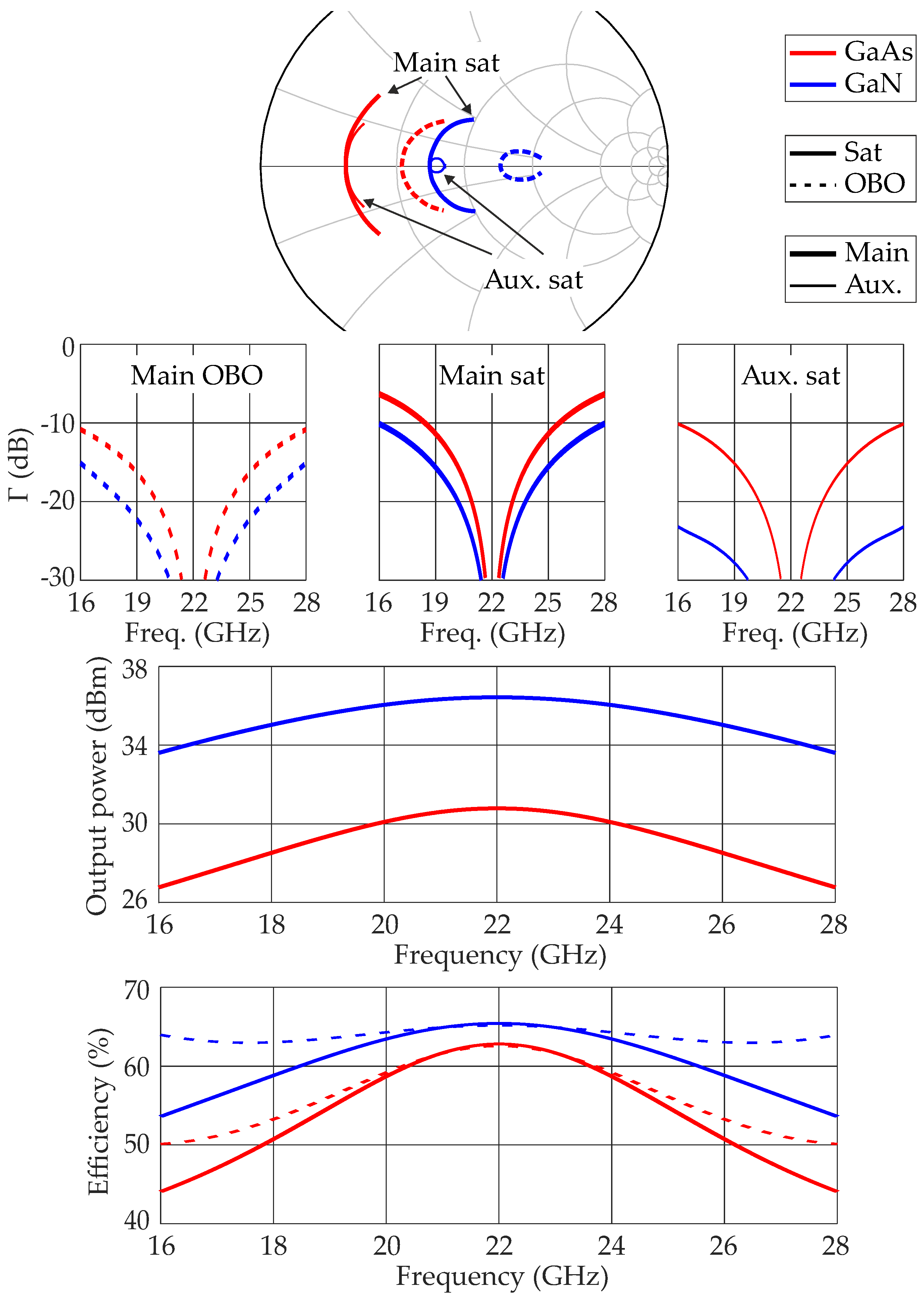
Figure 5 reports these quantities in the 16–28 GHz range, for the GaAs (red) and GaN (blue) combiners. Thanks to the higher
and consequently lower impedance transformation required to reach the external
, GaN results more wideband. This effect is visible and consistent in all quantities, current generator impedances, power, and efficiency. The absolute and relative bandwidths according to the 25% performance reduction criterion are reported in
Table 4. In both cases, this type of combiner allows maintaining better control of the auxiliary intrinsic impedance as compared with the main.
It is evident that GaN can achieve a much higher power with the same active periphery (6 dB higher, since the assumed power density is four times higher), while the maximum efficiency is almost equal in the two technologies, with a small advantage for GaN due to the lower impact of the knee voltage. However, in both cases, it is possible to maintain reasonably good performance over multi-GHz bandwidths.
3.2. On-Chip Power Combination Strategies in GaN
Given that the power levels required by the selected application can only be reached at the chip-level, adopting GaN, as anticipated in
Section 2, the several power combination strategies described are here explored in terms of frequency behaviour for the selected GaN technology. The active periphery of the individual transistor is 1mm and the adopted combiner is the one in
Figure 4 as above. The three considered topologies are shown in
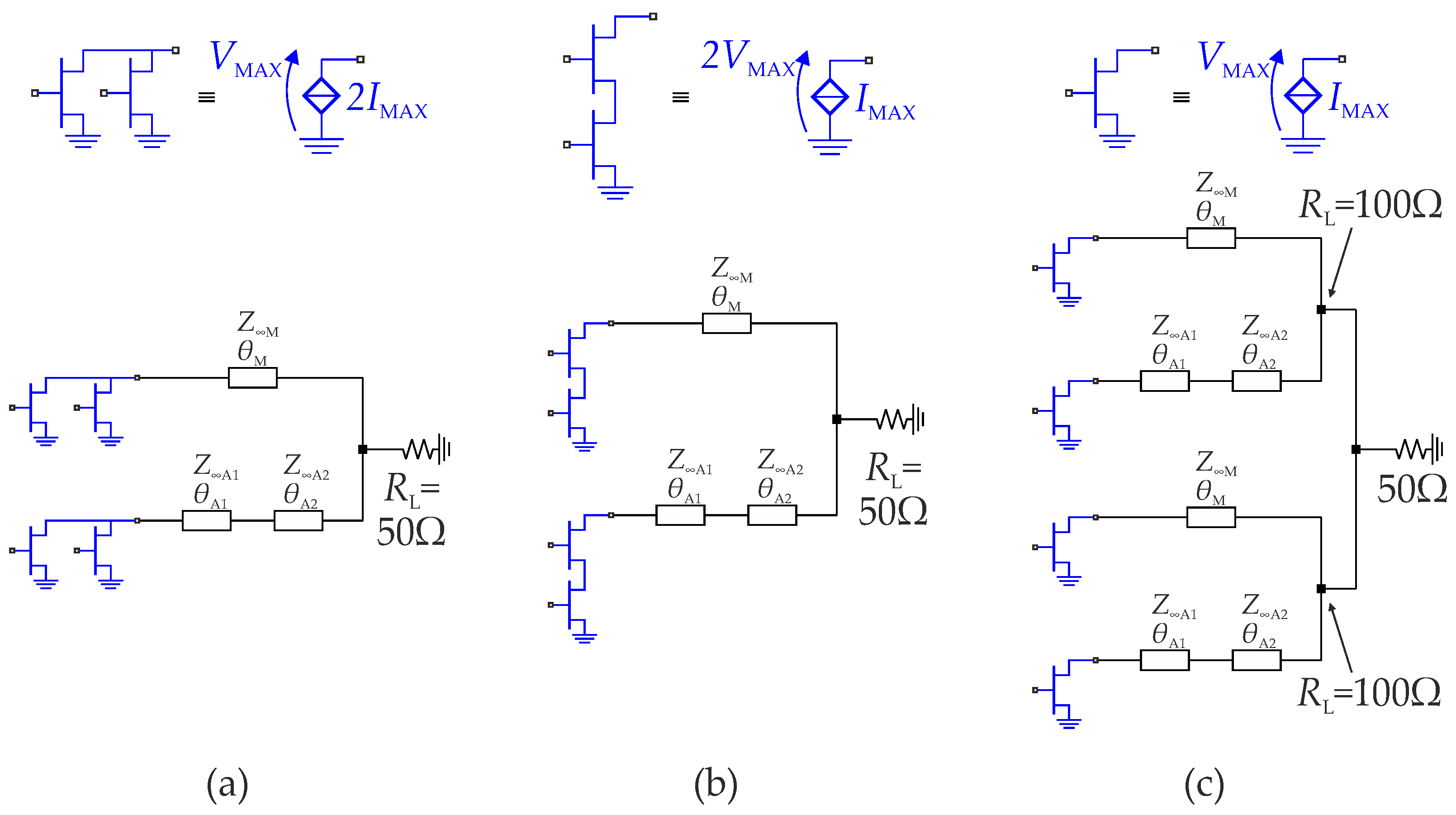
Figure 6, which also reports the equivalent current source representation of the transistors to be employed in the analysis in each case. As described in
Section 2, combining two devices in parallel ideally doubles their output current (a), while stacking them ideally doubles the output voltage (b), compared to the single-transistor case (c). The combiner parameters for these examples are given in
Table 5.
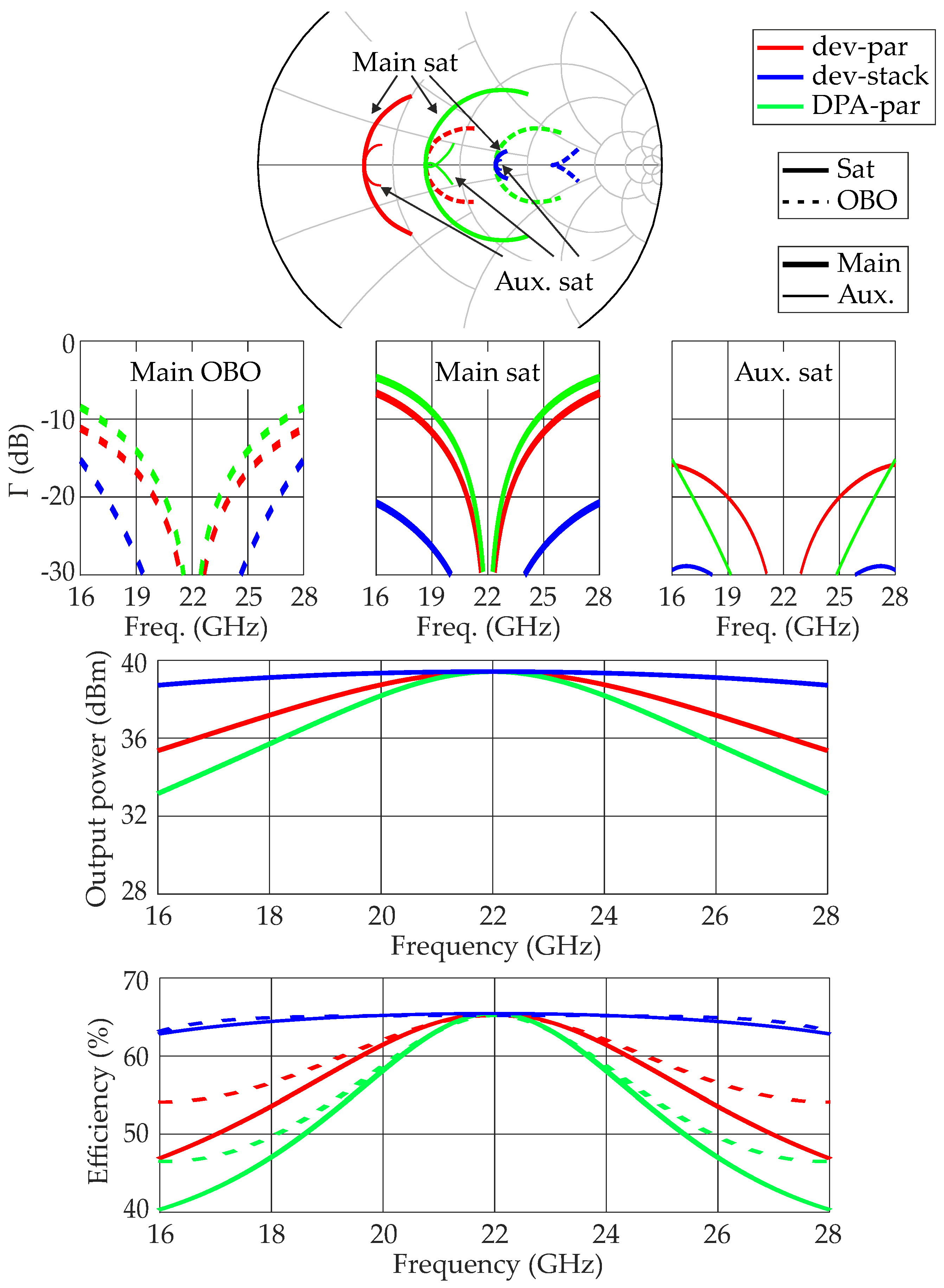
Figure 7 reports the current-generator impedance in the form of reflection coefficients, and reports the saturated power and efficiency, achieved when the power combination occurs at the DPA level (green), and at the device level, in parallel (red) or stacking (blue). Clearly, the output power and efficiency achieved at the center frequency are the same in all cases, since the technological parameters are the same and the design is exact at
. However, the different values of the impedance levels and of the transformation ratios,
r, lead to a marked difference in terms of frequency behavior. The combination at the DPA level results the least wideband, whereas device stacking provides very flat behavior versus frequency. In all cases, the saturated output power and the efficiency, both at saturation and at 6 dB OBO, have the same relative trends. The absolute and relative bandwidths, according to the 25% performance reduction criterion, are reported in
Table 5. While there is a mild difference between parallel combinations at the device and DPA-levels, the stacking of devices has a 50% relative bandwidth, roughly double compared with the other two cases. In terms of synthesized loading impedance, the trend of the main is the same as that of power and efficiency, whereas, on the auxiliary side, the parallel combination of DPAs allows maintaining the desired load on a wider bandwidth than the parallel combination of devices. This is, to some extent, a side effect, since the main typically has a stronger effect on the overall performance.
It can be noted that, despite having the same impedance transformation ratio , the parallel combination of devices and DPAs does not provide the same bandwidth. This is due to two related reasons: on one side, to the different impedance levels, and on the other side, to the different constraints in the selection of the free parameter. In fact, the DPA combination has higher impedance levels, which easily lead to high values of and . The combiner parameters that would provide the widest bandwidth would be unfeasible from a practical point of view. Therefore, in this case study, the parallel combination at the device level assures a more wideband behavior. Finally, thanks to the more favorable transformation ratio , the stacking of devices appears to be the most wideband solution, even more so than the DPA without any power combination.
3.3. Parasitic Effects
Some remarks relative to the qualitative observations just made are called for. In the simplified analysis of
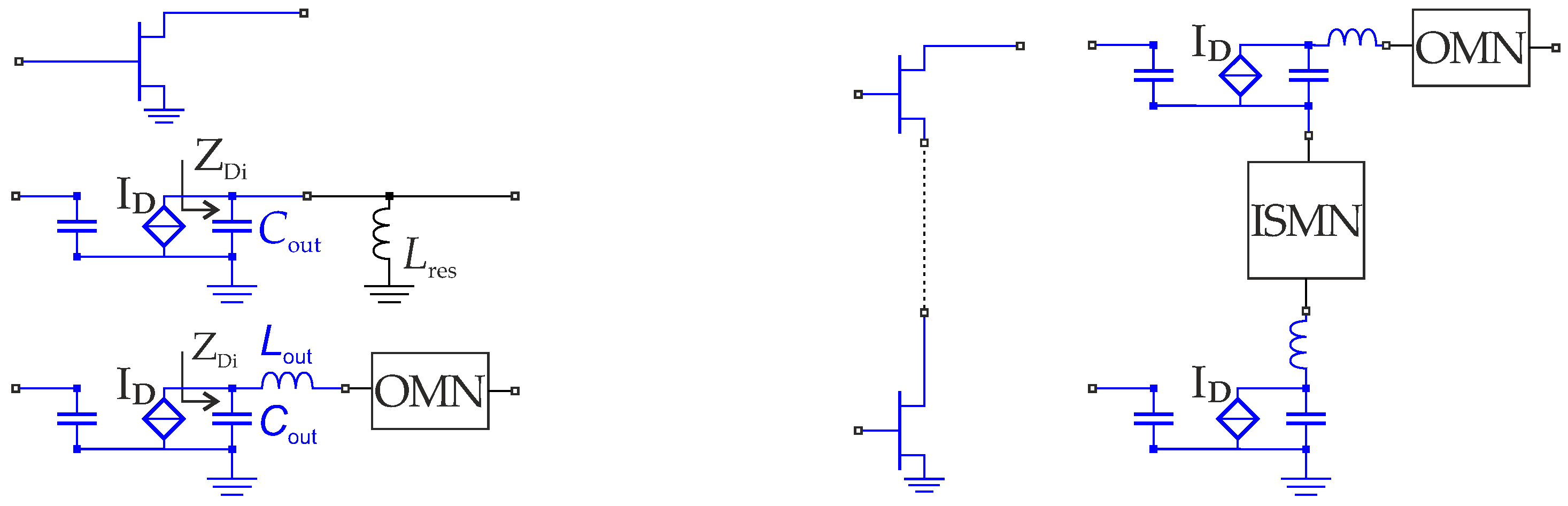
Section 3, the transistors have been modeled as ideal current sources for simplicity. However, the parasitic effects of the active devices of the considered technologies, and in particular the reactive ones, are not negligible in K bands and must, therefore, be considered and properly compensated for. The simplest possibility for the design of the output section of a PA is to model the device’s output as a shunt capacitance,
, which can be either resonated out by means of a shunt inductor, or embedded into the TL section—if its characteristic impedance is compatible—or compensated for by a generic structure. Another possibility, more accurate at these frequencies—especially if wideband operation is desired—is to model the device’s output as a shunt capacitance,
, followed by a series inductance,
, in which case the compensation network could be more complex than a simple inductive shunt element. The representation of the output parasitic effects of a transistor and the compensation thereof is summarized in
Figure 8 (left).
Other effects impacting the bandwidth that have been neglected in this example are, for instance, the passive structures that are required to physically connect the devices in the two device-level power combination strategies, both in parallel and stacked. These structures have a non-negligible impact on losses and bandwidth at these frequencies. In particular, the device stacking requires, besides the conventional compensation of the parasitic output effects of the devices, inter-stage matching networks to compensate for the parasitic effect of the top transistor on the preceding one (see
Figure 8 (right)). These effects are not easily accounted for in a linear analysis, which simply models a stacked cell as a current source with a doubled operating voltage.
The parallel combination of DPAs, as implemented here, on the contrary, has no extra parasitic effect, since single transistors are employed and the connection of the DPA cells at the output requires no additional physical structure. Additionally, this architecture is the one that lends itself more naturally to the implementation of a different type of Doherty combiner, i.e., the one based on the embedding of the output capacitance, which is typically more wideband.
The effect of the output parasitic effects of the transistors and of the type of combiner adopted is illustrated by the the parallel combination of DPAs (case “DPA-par” of
Figure 7). An output capacitance—
fF—is added in parallel to the main and auxiliary current, which is a reasonable value for the selected technology, based on [
25,
26]. The case in which
is resonated out by means of a shunt inductance at
is compared to the case in which
is embedded into the combiner. In the former, the combiner is exactly that of
Figure 4 and the parameter values are those listed in
Table 5. In the latter, the TL sections connected to the transistors are implemented by means of an equivalent
network (shunt capacitance–series inductance–shunt capacitance), whose leftmost element is
itself, and there is a post-matching section between the common node and the actual
. The details for the design of this type of combiner can be found in [
13,
32].
Figure 9 reports the frequency behavior in the resonating (red) and embedding (blue) cases. It stands out that the embedding combiner has a strongly asymmetric response, and therefore designing it at center frequency is not the optimum choice. However, this topology offers the possibility of designing a wideband DPA, even at frequencies where the parasitic effects of its devices are non-negligible, despite the challenging impedance transformation ratio. The improved frequency response is especially visible in the saturated power, but also the achievable efficiency turns out to be higher away from the center frequency.
Table 6 reports the 25% absolute and relative bandwidths for these two cases. Considering the effect of
, and that resonating it out reduces the relative bandwidth from 18% to 14% compared with the analogous case—adopting an identical combiner but without parasitics (
Table 5). Instead, the embedding strategy allows achieving a 24% relative bandwidth.
Therefore, it can be concluded that a DPA based on the combination of two individual DPA cells can indeed achieve wideband operation if specific design choices are made. Furthermore, many degrees of freedom are available when designing an embedding combiner, including the topology of the post-matching network and its design frequency, and the possibility of implementing the elements’ equivalent
networks of the TL in lumped or distributed form. This opens a variety of possibilities the complete investigation of which is outside the scope of this work, but which can potentially improve the frequency behaviour of this topology beyond what is shown in
Figure 9. Indeed, the example shown in
Section 2 under the name MMIC2 has been designed using this linear analysis as a guideline and an optimization tool, adopting an embedding combiner where all the TL sections are implemented as
networks with lumped shunt capacitors and sections of TLs acting as series inductances, and where the post-matching network is a two-stage structure specifically optimized to maximize the flatness of the frequency response. The resulting DPA is expected to cover a bandwidth of over 3 GHz, around 18.8 GHz.


