1. Introduction
Power converters and their controllers are becoming more complex, especially since GaN or SiC semiconductors were integrated into this field, and the switching frequency increased drastically. Furthermore, power electronics are increasingly applied to electrical systems that are bigger and more complex than power converters [
1]. This complexity invokes the necessity of finding some reliable, economical, fast, non-destructive, and yet at the same time, accurate methods to test several critical scenarios encountered in real-world systems.
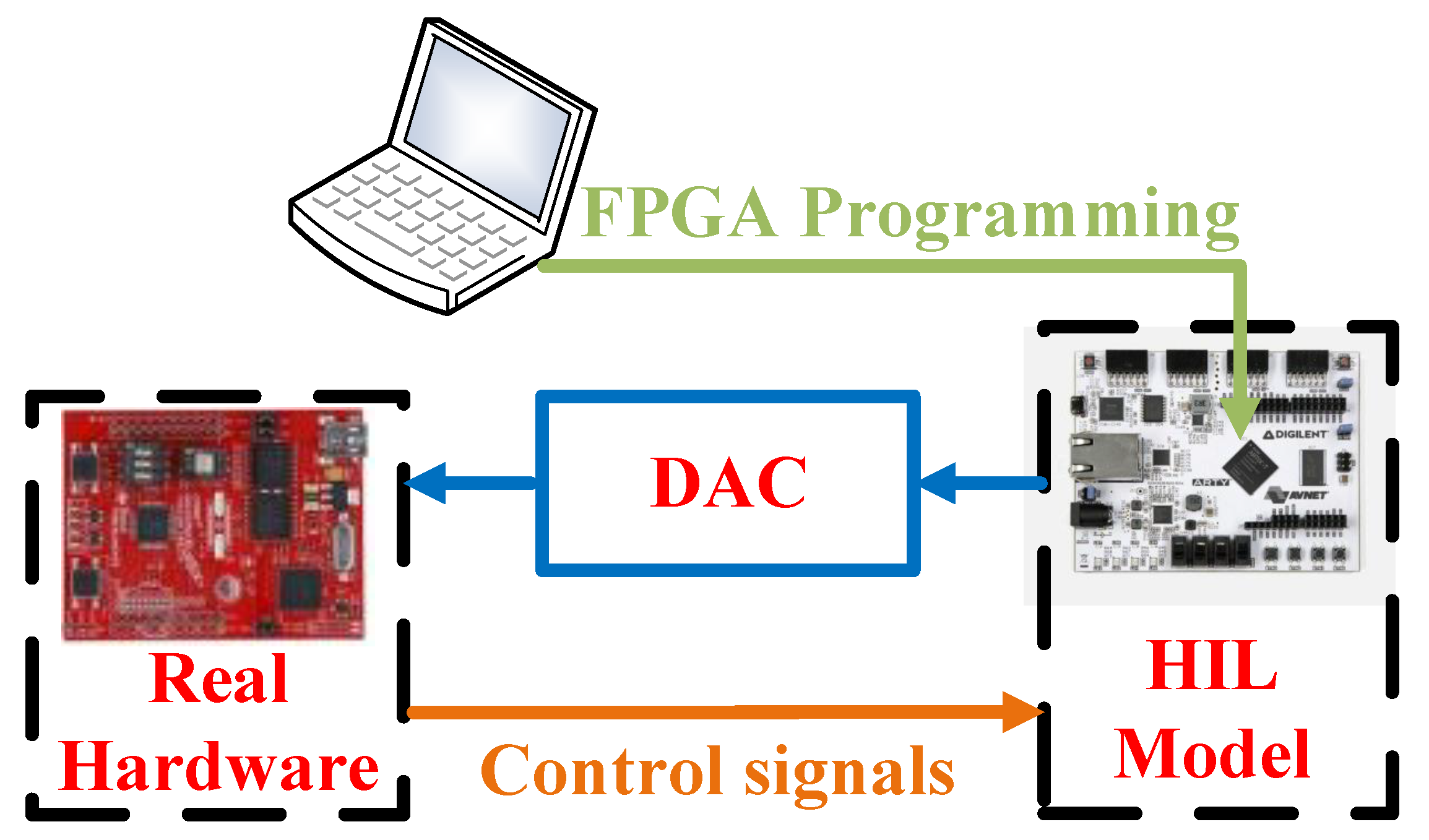
Recently, using the hardware-in-the-loop technique (HIL), it became possible to emulate parts of the system (controllers and power converters) using digital hardware in a non-invasive condition. The HIL model aims to imitate the behavior of real converters so it can be a substitute for them and interacts directly with the controllers in real time (RT), so the rest of the system is not aware if the converters are the real ones or HIL models [
2,
3], as shown in
Figure 1. In order to do that, there are two requirements: that the HIL model is executed in RT, and that it presents the same interface with the controller. Therefore, an HIL model must generate its outputs as analog signals through digital-to-analog converters (DAC) and read the controller commands through the on/off signals that control the switches. Regarding the implementation of the HIL models, it can be based on any digital hardware capable of implementing the equations of the model, ranging from computers to Field Programmable Gate Arrays (FPGAs). This paper will focus on FPGA implementations, as explained later. HIL models can be used to test different controllers to reduce the cost of debugging, avoid any damage to the real system, and reduce the overall test effort [
4,
5].
For numerous power electronic applications that operate with a switching frequency in the range of hundreds or even thousands of kilohertz, fast responding time from the HIL simulator is vital to model higher switching frequency converters or interact with them [
6]. Therefore, an advanced HIL system must be able to calculate the model quickly [
7,
8]. Apart from the necessity to reach the simulator’s speed response, as it was discussed in [
9,
10], reducing the simulation step in HIL models results in increasing the accuracy of them. It was shown in [
11] that the simulation step is proportional to the model’s error, so reducing it is usually the best approach to raise accuracy. The simulation step is recommended to be at least 100 times less than the switching period for keeping the precision [
11]. However, it is hard to reach that goal in mid-high-frequency HIL applications due to the minimum latency needed for executing the model equations [
12].
HIL systems based on microprocessors have been proposed for power converters in the frequency range of less than 10 kHz [
13]. However, it is nearly impossible to use microprocessors for high-frequency power converters in RT because of the small needed simulation step. For instance, a digital signal processor (DSP)-based HIL system for power converters such as Boost converter with a time step of
s was proposed in [
14]. Using the rule of 100 simulation steps per switching period, that would limit the switching period to a minimum of 100
s and therefore switching frequencies under 10 kHz.
The solution is using Field Programmable Gate Arrays (FPGAs), which have excellent parallel processing capabilities and low latency [
15]. A detailed comparison between DSP and FPGA boards for a voltage source converter-based static compensator application is presented in [
16] including the price and the advantages of each option. FPGAs can compute all equations in parallel with a short execution time that makes them ideal for fast RT emulation of power converters [
17,
18]. Just as a comparison, in [
19], an FPGA-based RT platform for power converters was presented, which achieved a time step of 200 ns for simple models. It was claimed that even for more complex models of power converters, the time step is less than 650 ns. Apart from FPGAs’ advantages, designers must take a set of constraints into account for FPGA-based RT applications, such as timing and FPGA implementation constraints, which was highlighted in [
20].
The minimum achievable clock period and hardware resources in FPGAs are affected by the used numerical format (NF), which will be discussed in this paper. A detailed comparison including the synthesis results and the accuracy using several NFs is proposed in [
21] which uses hardcore floating-point (FlP) DSPs available in Intel Arria 10 FPGA family. However, such hardcore DSPs are not available in most FPGA families. It is proven in [
21] that FlP is much slower and less accurate than fixed-point (FxP) in some applications, although it needs less design effort. A similar comparison is also proposed in [
22] for FPGA-based electrical machines implementation, showing that FlP computation may not lead to more accurate results than FxP in RT simulation.
Apart from the NF, the synthesis tools used to implement the models in FPGAs, and design approaches such as using intellectual properties (IPs) in FlP can affect the area and speed [
23]. A comprehensive comparison of HIL systems and other design alternatives is presented in [
24] including the System Generator tool to translate high-level codes into synthesizable code in FPGAs. It shows that System Generator—which translates M-code of MATLAB/Simulink into synthesizable hardware description language (HDL) code for Xilinx FPGAs—results in more resources and longer simulation step (about 50%) compared to hand-coded implementation for a Boost converter without losses [
24]. However, that research uses an old FPGA, and also the software tool (ISE) is deprecated presently.
Several synthesis tools support different input languages (VHDL, Verilog, C, etc.). In this paper, Vivado and Precision are used as synthesis tools. These tools offer their internal optimization and give different results, even for very similar input descriptions. Hence, it is challenging to compare their performances and find a trade-off between hardware implementation with different complexity and NFs.
When designing digital circuits, the first step is to prepare a device architecture description by codifying the system’s behavior, making it possible to standardize the design process. The models can be codified at Register Transfer Level (RTL) using HDL languages, such as VHDL [
25,
26] or Verilog [
27,
28]. However, the handcrafted HDL code needs remarkable design effort because it must specify the functionality at a low level of abstraction, where cycle-by-cycle behavior is entirely determined. The model can be created in MATLAB/Simulink to reduce the design effort, and it can be translated into HDL code using MATLAB HDL coder or System Generator if the target device is a Xilinx FPGA. For instance, the HDL code of a back-to-back IGBT-base converter was obtained in [
29] using MATLAB/Simulink HDL Coder.
Another possibility to codify the models is using high-level synthesis (HLS) languages such as C, C++, or System C [
30,
31]. HLS can be used to design FPGA circuits, where hardware implementations can be easily described and replaced in the target device using shorter and more abstract structures instead of using verbose and extremely detailed HDL structures [
32,
33]. HLS can accelerate the design process and improve flexibility because the code can be translated directly into HDL using, for example, Xilinx Vivado HLS. However, the abstraction of high-level languages can lead to worse synthesis results. An HLS tool to develop FPGA-based RT simulators for power converters has been studied in [
34] with a conclusion that the time step would be enormous for RT applications. It would use almost all the FPGA resources if the model is complex.
Recently, some commercial HIL platforms such as Typhoon HIL [
35], Opal-RT [
36], and National Instruments (NI) RIO family [
37] have appeared to implement HIL models. The latter, programmed through LabVIEW software, is used for several applications, not only HIL. In this paper, NI myRIO synthesis results are achieved as a possible solution to implement HIL models using a common commercial tool.
The objective of this paper is to compare different design alternatives for HIL when the implementation is going to be based on FPGAs. FPGAs are the only option for HIL models of mid-high switching frequency converters (around hundreds of kHz or higher), but of course can also be used for lower switching frequencies. Once the choice of using FPGAs for implementation is taken, there are a lot of design alternatives, such as NF, design language, or synthesis tools. The purpose of this paper is to present a comprehensive comparison of these alternatives so the designer can take the most appropriate alternative for each application. Although the paper presents two implementation examples, the intention is to give general guidelines that should be valid for any power converter. In fact, similar conclusions could be extracted for other applications apart from power converters.
The rest of this paper is organized as follows: In
Section 2, a brief explanation of how to model two different power electronic converters (a Buck converter without losses and a Full-bridge converter with losses) is shown, and the equations are obtained.
Section 3 introduces several possible design approaches and synthesis tools that have been used for the implementation of HIL models in an FPGA. The experimental results and a complete comparison in terms of area, time, and design effort are accomplished in
Section 4. Finally,
Section 5 provides conclusions.
3. Design Possibilities for Implementation of HIL Models in an FPGA
There are several possibilities to implement HIL models in an FPGA regarding different NFs, coding possibilities, and synthesis tools. This section proposes an assortment of design alternatives of HIL models for power converters. The first election lies in deciding between FlP and FxP numerical formats, which are the two most used formats for digital systems.
Different coding possibilities are also available for each NF, which will be introduced in
Section 3.2. Notably, not all different coding languages are supported by every synthesis tool, so the synthesis tool selection is not entirely free in all cases. However, when more than one synthesis tool is possible, not all of them lead to the same results in terms of area and delay, so the impact of synthesis tools is also analyzed.
3.1. Numerical Formats
Equations (
1) to (
5) must be implemented in FPGA to imitate the converters’ behavior in RT. Two different synthesizable NFs (FlP and FxP) are used for any FPGA-based hardware design, while the design effort, accuracy, area, and time results can be different.
The fundamental FlP formats provided in the IEEE-754 standard are 16-bit half-precision, 32-bit single-precision (SP), 64-bit double-precision, and 128-bit quadruple-precision. The most common NF for a wide range of digital electronics applications is the SP FlP format, which can be the first choice for designers because of its flexibility and user-friendliness. All signals in this NF use 32 bits, and it can be implemented in VHDL-2008 float_pkg package. In FlP format, each number contains a sign, exponent, and mantissa. The sign bit can be either ‘0’ or ‘1’ for positive or negative values, respectively, while in the case of SP format, the exponent is represented in 8 bits, and the mantissa is a 23-bit integer number. Using SP FlP format, an extended dynamic range of numbers (values up to ) can be represented, and the model usually will not face underflow or overflow issues. Regarding resolution, as there are 23 mantissa bits, the resolution is multiplied by the maximum representable number for a given exponent. For example, if the capacitor voltage is 100 V (), its resolution would be V. The main reason for using the SP format is its reasonable trade-off between resolution and required resources for FPGA implementation in comparison with other FlP formats.
Apart from FlP, the other NF is FxP. The FxP format can be the best choice for RT emulations when small simulation steps (higher resolution) are needed because FxP needs fewer resources than FlP, obtaining shorter clock cycles (faster execution). The FxP NF is a variant of the typical integer representation (2’s-complement signed in this study) where a point location is fixed, splitting the integer and the fractional parts of the number. The designer must decide the number of integer and fractional bits for FxP, which is not trivial. This format can be specified with two integer numbers (QX.Y), where X depicts the number of integer bits while Y represents the number of fractional bits. A total of bits are used to include the sign. Each FxP variable can store values up to with a resolution of .
The main advantage of FlP is the smaller design effort compared with FxP. The point location of different FlP variables is shifted dynamically by changing the exponent field of the number. Thus, there is no need to calculate in advance the number of integer and fractional bits for different signals. Therefore, the designer just declares all signals in the model as SP FlP, being a code easy to generate, read and maintain. Moreover, after designing the model in FxP, it can work only in a specific numerical range because the number of integer bits is determined, while in FlP, the point location can be shifted automatically. Therefore, given these advantages of FlP over FxP, FlP is the natural choice when the obtained performance is enough. However, FlP operations have longer latency and require more logic resources to be implemented in FPGAs. For example, the FxP model of a synchronous Buck converter proposed in [
42] achieves a three times smaller simulation step in FxP than in FlP. Similar results are obtained in this paper, as will be shown in
Section 4. FlP finds a barrier to reach simulation steps under 50 or 100 ns. Following the rule of 100 simulation steps per switching period, that would indicate that FlP models can only be used for switching frequencies under 200 kHz approximately. Apart from shorter simulation steps, FxP models use fewer resources, so a designer may opt to use FxP when models are big, complex, or area becomes critical because of cost reasons.
Regarding resolution, SP FlP should have enough resolution for most applications. There is an exception found in [
24], where the resolution of an SP FlP model of a Boost converter used in Power Factor Correction was demonstrated to be not enough. However, FxP allows optimizing the trade-off between hardware resources and resolution since the resolution of each individual signal is decided during the design phase. Deciding the optimal resolution is a topic beyond the scope of this paper. More details about resolution issues for both FlP and FxP can be found respectively in [
43,
44,
45].
In this paper, a Buck and a Full-bridge converters’ models are proposed, which can be implemented in FPGAs to compare different design alternatives for both FlP and FxP numerical formats. Word length optimization for the FxP format has been studied to avoid overflows, optimize the hardware, and keep the accuracy [
46,
47]. The main contribution of this paper is the comparison of the synthesis results obtained by different design approaches for implementing the same model, regardless of the used signal format, to reveal the differences between several design alternatives. In this study, the signal width in the proposed FxP models is selected based on [
44] to save hardware resources for computational processing and at the same time to have a reasonable error. It is notable that in the case of SP FlP, the format is always 32 bits as defined in the standard
IEEE-754. Thus, there is no need to determine the width of the signals.
3.2. Design Approaches and Tools
After choosing the NF, the next step for the designer is to codify the model of the converter in a language ready for FPGA synthesis. This task consists of translating Equations (
1) to (
5) into code. For the Buck converter, the Pseudocode would be the following one:
if q is on {
vL = Vin − vo;
}
else {
if q is off and iL ≤ 0 {
vL = 0;
} else {
vL = −vo;
}
}
iC = iL − iR;
iL = iL + vL ∗ dtL;
vo = vo + iC ∗ dtC;
while for the Full-bridge the Pseudocode would be:
if (q1 is on) and (q3 is on) {
vL = Vin − vo − (2 ∗ Rdson + RL) ∗ iL;
} else if (q2 is on) and (q4 is on) {
vL = − Vin − vo − (2 ∗ Rdson + RL) ∗ iL;
} else if (all qs are off) and (iL > 0) {
vL = − Vin − vo − 2 ∗ VD ∗ sign(iL) − (2 ∗ RD + RL) ∗ iL;
} else if (all qs are off) and (iL ≤ 0) {
vL = Vin − vo − 2 ∗ VD ∗ sign(iL) − (2 ∗ RD + RL) ∗ iL;
} else if (only q1 or q3 is on and (iL > 0) {
vL = − vo − VD ∗ sign(iL) − (Rdson + RD + RL) ∗ iL;
} else if (only q1 or q3 is on and (iL ≤ 0) {
vL = Vin − vo − VD ∗ sign(iL) − (Rdson + RD + RL) ∗ iL;
} else if (only q2 or q4 is on and (iL > 0) {
vL = − Vin − vo − VD ∗ sign(iL) − (Rdson + RD + RL) ∗ iL;
} else if (only q2 or q4 is on and (iL ≤ 0) {
vL = − vo − VD ∗ sign(iL) − (Rdson + RD + RL) ∗ iL;
}
iR = GL ∗ vo;
iC = iL − iR;
VRESR = RESR ∗ iC;
iL = iL + vL ∗ dtL;
vC = vC + iC ∗ dtC;
vo = vC + VRESR;
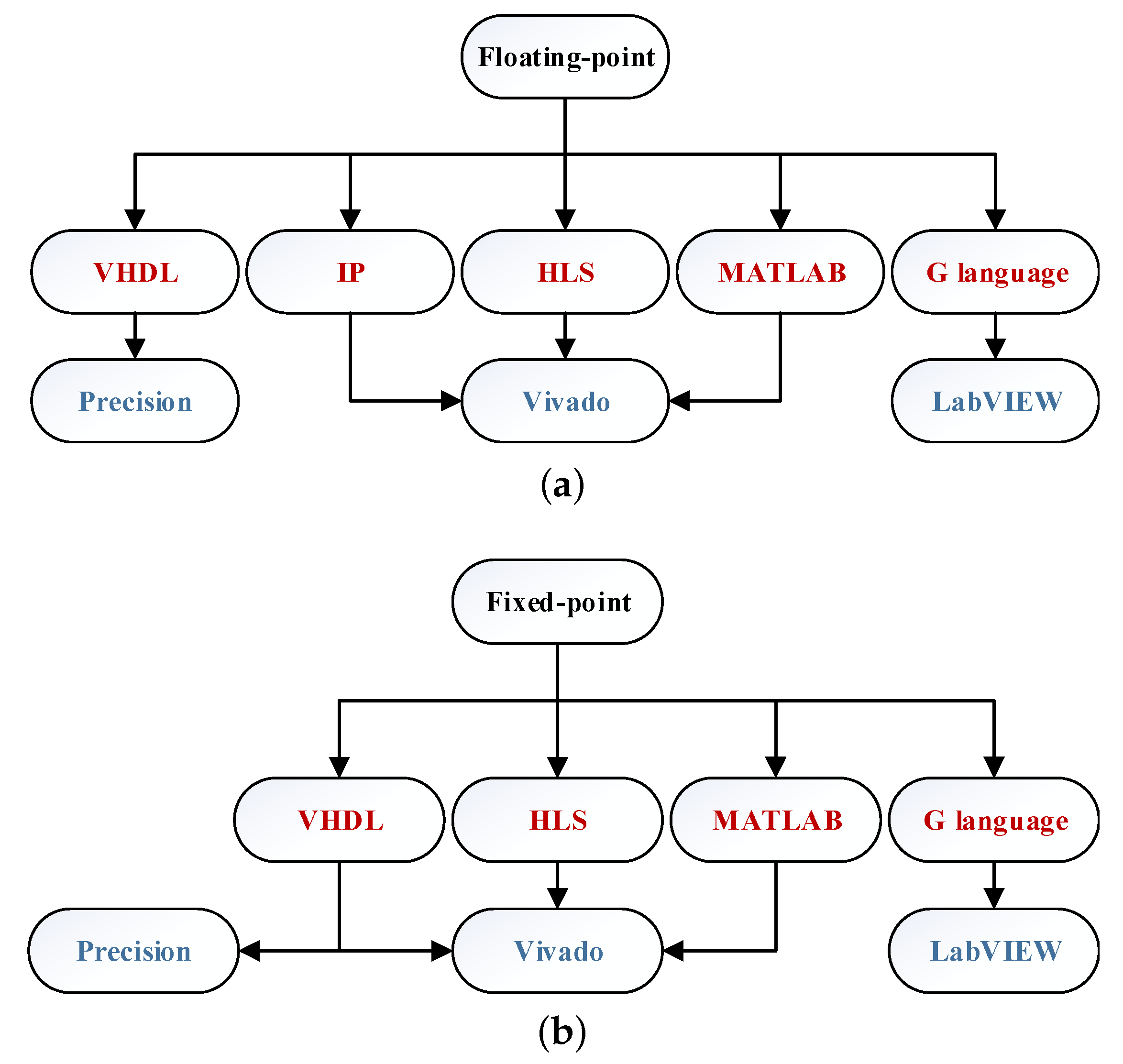
Now the question is which language to use for implementing the Pseudocode in synthesizable code. Furthermore, not all languages are supported by any synthesis tool, so pairs language-synthesis tool must be considered. The selection of the language to be used is not just a question of the designers’ knowledge or preferences but also impacts both design effort and hardware resources, even for the same FPGA-based HIL model. Five different approaches (VHDL, IPs, HLS, MATLAB, and graphical language (G language)) are considered to codify the converter’s model, although all methods are not available for both NFs.
Figure 3 shows all the possibilities explored in this paper regarding NF, coding method, and synthesis tools.
The first approach to codify the model can be using the VHDL language. By the moment, the IEEE VHDL-2008 FlP standard library is not supported by Vivado, as Vivado is not fully compatible yet with the standard VHDL-2008 [
48]. The alternatives for FlP implementation in VHDL using Vivado would be using non-standard FlP libraries or hand-coding FlP arithmetics. These options require further knowledge from the designer and much more effort for hand-coded FlP implementation, so the proposed alternative is simply to use another synthesis tool that does support IEEE VHDL-2008 FlP standard libraries, like Precision from Mentor Graphics.
The next approach uses IPs provided by the FPGA vendors, which are ready-to-use solutions for FlP units and can be one of the main components in any computing architecture. IPs implement arithmetic operations, but to do so, they must be instantiated. So, the difference in the code would be from:
Q <= (A + B);
to:
Adder1 : floating_point_adder(
In1 => A,
In2 => B,
Output => Q
);
So, IPs increase the syntax overhead and make the code less human-friendly, but they can be a good option for optimum synthesis results. Most operators’ latency using IPs can be set between 1 clock cycle and a maximum number that depends on the chosen parameters. However, pipeline structures are not recommended in this application because each step’s results are fed back to the next step, so all IPS must be configured as fully combinational at the expense of increased hardware resources.
The third coding possibility, apart from VHDL and IPs, is HLS. High-Level Synthesis included in all Xilinx Vivado HLx Editions can support both NFs by transforming C functions written in C, C++, or System C into an RTL implementation to be directly integrated into Xilinx FPGAs. For the results of this paper, the Pseudoce has been codified using C++. The Vivado HLS tool can translate high-level codes into synthesizable code automatically. However, it is not the only possibility to avoid an arduous hand-coded VHDL or IP approach.
To get rid of the design effort caused by hand-coded HDL, Equations (
1) to (
5) can also be written in M-code files (MATLAB language), and HDL Coder can be employed to translate them into VHDL codes. Using HDL Coder, the model can be configured by selecting the target device (e.g., Xilinx Artix FPGA) and the pipeline technique’s usage level (no pipeline). These two last coding methods (HLS and MATLAB) reduce the differences between software programming and FPGA programming. Therefore, using these approaches, many details such as time schedule and low-level implementation are abstracted.
All the previous methods are based on codifying the equations of the converters (
1) to (
5) in different text languages and tools. The last analyzed alternative is to codify the converters’ equations using a graphical language (G programming language) instead of a written language. In this approach, the LabVIEW environment automatically connects to the synthesis tool, making the process transparent to the user, including downloading the design to the FPGA. However, the choice of target boards is restricted to NI platforms (CompactRIO, sbRIO, roboRIO, FlexRIO, NI R Series, and NI myRIO-1900).
4. Results and Comparison
This section compares the different possible design approaches previously introduced, quantifying the differences, such as hardware resources and the minimum simulation step. Furthermore, the design effort and the accuracy of all tested design alternatives are compared to help developers decide on the appropriate design option based on the application.
The models explained in
Section 2 have been implemented in a Digilent Arty 7-35T development board, which includes a Xilinx Artix-7 FPGA, model xc7a35ticsg324-1L. This FPGA includes 5200 slices (every slice comprises four 6-input Look-Up Tables (LUTs) and eight flip-flops (FFs)) and 90 DSP blocks. The models coded in G language have been implemented into the NI myRIO-1900 platform (see
Figure 4), which includes a Xilinx Zynq-7010 FPGA. Although they are different FPGAs, the Zynq-7000 family uses the same fabric logic of the Artix-7 family, so the synthesis results are very similar in both families, as will be shown later.
4.1. Floating-Point Discussion
As explained in
Section 3.2, the FlP models of the Buck and Full-bridge converters are written in VHDL and verified only with the Precision tool because the standard VHDL-2008 IEEE FlP library is not supported by Vivado. The implementation results for the FlP VHDL models will be presented and compared with other design possibilities.
The proposed models using IPs (Xilinx Floating-point IP, version 7.1 (Rev. 7)) are also available, and it is expected that the usage of IP cores can improve the synthesis results. However, different configurations for FlP IPs are possible, resulting in a quite different resource usage and minimum RT simulation step, as shown in
Table 1. All IPs in the proposed models, which implement additions, subtractions, and multiplications, use single-precision and are configured as purely combinational (no pipeline). The architecture optimization of add or subtract IPs can be chosen between
high-speed and
low-latency, affecting the synthesis results. For multiplications, there is an additional parameter to be chosen, which is how many DSP blocks are used per multiplication.
Table 1 provides an assessment of different IPs configurations in terms of the number of LUTs, FFs, DSP blocks, and the minimum achievable clock period (
, which is equal to the simulation step because the simulation step is solved in a single clock cycle) to find the best IP configuration for implementing the HIL models in RT. It should be taken into account that these HIL models are fed back, i.e., the result of the capacitor voltage is used for the calculus of the inductor current and vice-versa. Therefore, the only important parameter is the total latency of the calculus. That is why it is recommended to use a single clock cycle which is equal to the simulation step of the model, so no pipeline is used. As listed in
Table 1,
low-latency IPs with the
maximum usage of DSP blocks reach the minimum possible clock period and hardware resources for both converters. Thus, this IP configuration, which is highlighted in
Table 1, will be used in the rest of the paper to compare the IP solution with other design alternatives for FlP.
Apart from pure VHDL and VHDL with IPs, other design alternatives are to obtain the models in high-level languages and implement them from a higher level of abstraction. In this study, Equations (
1) to (
5) written in C++ and MATLAB language (M-code) are implemented into an FPGA using Vivado HLS tool and MATLAB HDL Coder plus Vivado, respectively. The last discussed FlP design possibility is to use LabVIEW for programming the NI myRIO-1900 platform as a commercial HIL tool.
Table 2 shows the synthesis results of various FlP design alternatives of the Buck and the Full-bridge converters. It can be seen that although using FlP IPs consumes fewer hardware resources and reaches a smaller emulation step than other approaches to implement the Full-bridge model, the synthesis results of IP and HLS approaches for Buck converter are very similar. It can also be observed that using the standard FlP library of VHDL-2008 and Precision synthesizer, the necessary resources and the minimum achievable clock period are increased in both converters. The reason may be a low optimization of the FlP library or the low optimization of the Precision synthesizer for Xilinx FPGAs. Nevertheless, this synthesizer is required since Vivado does not support that library by now, as was commented before. Automated MATLAB HDL code enhances synthesis results and time steps compared with the pure VHDL approach. However, compared to other design alternatives, it needs more area and reaches a greater time step, especially for complex models.
LabVIEW FPGA uses a fixed amount of myRIO’s programmable FPGA resources to be ready for implementing any possible design. An empty virtual instrument (VI) occupies 64.7% of the total available resources in the myRIO’s FPGA. Thus, the available resources are limited, and complex models cannot be implemented in this device, especially the FlP models that need more hardware resources. As shown in
Table 2, the float model of the Full-bridge converter with losses cannot fit into the myRIO’s FPGA. The number of available slice LUTs is 17600; however, the Full-bridge converter’s float model needs 27,227 slice LUTs.
The synthesis results’ analysis demonstrates that the LabVIEW-myRIO approach occupies more FPGA area than other design alternatives introduced previously, and it is not as fast as them. However, it is possible to download and debug the model using a graphical interface, and also the virtual oscilloscope is included in LabVIEW to monitor the model implemented into the FPGA. Furthermore, using the front panel in LabVIEW software, designers can interact with the model to change and control different parameters while the model is running.
The same test has been accomplished disabling DSP blocks to determine the impact of DSP blocks on the area and maximum achievable clock frequency. However, it is not supported by LabVIEW, and Vivado HLS does not fully support non-DSP FlP implementation, so it works only partially, as can be seen in
Table 2. It should be noted that synthesizing without using DSP blocks is not recommended because it will increase the minimum clock period; however, these results are useful for comparing the total combinational area, which comes from both LUTs and DSPs. For instance, VHDL-Precision uses more LUTs but fewer DSPs than the IPs-Vivado approach. However, when disabling the DSPs, so all the combinational logic is implemented through LUTs, it becomes clear that VHDL-Precision uses the most resources, and that is also the reason for its worse time results.
4.2. Fixed-Point Discussion
In this section, four main coding possibilities (VHDL, HLS, MATLAB, and G language) to implement the converters’ FxP model in an FPGA are tested. Unlike FlP, the model using the VHDL-2008 IEEE standard FxP libraries can be synthesized using both Precision and Vivado.
Apart from the design possibilities mentioned before, the methods used for limiting the number of digits (bits in binary) impact the trade-off between accuracy and hardware resources. From now on, these methods will be called NBL (number of bits limitation), which can affect the right or left bits. For instance, when limiting the number of bits in the right (least significant bit or LSB), FxP can use rounding toward the nearest value (choosing the nearest solution with a limited number of fractional bits, option by default) or truncating (eliminating the right bits). Of course, rounding is more accurate but demands more hardware resources. In the same way, when the number grows beyond the range limit of the chosen FxP format (overflow in the left or most significant bit, MSB), FxP can saturate (choose the nearest solution with a limited number of integer bits, option by default) or wrap (eliminate the left bits, which leads to entirely different solution). Again, saturating is more accurate but demands more hardware resources than wrapping. Therefore, the two extreme NBL options would be rounding and saturating (RS) for maximum accuracy but using more hardware resources and truncating and wrapping (TW) for minimum hardware resources.
The RS method tries to reduce the error using two techniques: the rounding increases the resolution of the number in 0.5 bits virtually, and the saturation prevents the value from being overflowed without using one extra bit, obtaining numerical error but less than in an overflow condition. An alternative is not using any of those methods but using directly two-guard bits.
Applying two-guard bits to the TW method (TW + 2), one for the integer part to avoid overflow and the other one to the fractional part to avoid inaccuracy, can be the third NBL method to have the benefits of both previous methods. In this section, a comparison between the three commented possibilities has been carried out to find the optimum NBL method for HIL models to provide a more accurate and efficient model. To avoid overflow and reach acceptable precision, all signal widths are chosen based on the algorithm proposed in [
45]. However, different NBL methods are included in three different tests to compare needed hardware resources and the achievable clock period regarding different design methods.
The comparison of synthesis and timing results for different NBL methods of FxP models for both converters are shown in
Table 3,
Table 4 and
Table 5 when using VHDL with Precision, VHDL with Vivado synthesizer, and HLS, respectively. As expected, the TW method always needs fewer resources than using RS. The synthesis results show that although the RS method offers a higher level of accuracy than the TW method, an increase in HIL models’ minimum achievable clock period increases the error at each time step. As shown in [
11], the HIL model’s error is basically proportional to the clock period. Consequently, the RS method may reduce the RT emulation results’ accuracy and increase the final cost of the models implemented in FPGAs. If the TW method’s obtained accuracy is not good enough, it is better to increase the number of bits (TW + 2) than using RS. TW + 2 method may guarantee more accurate results because, as shown in
Table 3,
Table 4 and
Table 5, it reaches a smaller clock period with fewer hardware resources than the RS method, although the mathematical error is very similar to the RS method. Thus, in the following, TW + 2 is used to compare different FxP design alternatives.
Synthesis and timing results of different FxP design alternatives using the TW + 2 method are summarized in
Table 6. As can be seen, the simple model results (Buck converter without losses) are quite different from the complex model (Full-bridge with losses). It can be concluded that for simple models, using different FxP design alternatives results in a very similar achievable clock period (about 12 ns), while HLS and MATLAB approaches need more hardware resources. Moreover, the timing results of the LabVIEW approach are the worst. As can be seen, the FxP Buck converter implemented in NI myRIO hardware is 12.5 times slower than the HLS approach. The timing results are even worse for the Full-bridge converter than the FxP Buck converter if the model is coded in G language (LabVIEW).
As listed in
Table 6, disabling DSP blocks, the Buck model uses 2600, 2018, 1022, and 740 LUTs for HLS, automated MATLAB HDL code, VHDL synthesized in Vivado, and VHDL synthesized in Precision, respectively. Thus, the optimum alternative for simple designs can be selected based on the simplicity of the design process or the available developers’ choices as the area and clock period differences can be neglected.
Notably, the HLS and MATLAB coding methods need less programming effort, but the latter needs more software and hardware requirements. In a short word, according to less design effort of the HLS approach, it can be the best option to design simple FxP models.
Nevertheless, the HLS approach reaches a significantly higher clock period for complex systems (about 32 ns for the Full-bridge converter with losses while the other methods are around 20 ns) and requires more hardware resources than other design possibilities. The complex models codified in VHDL-2008 (using both synthesizers) or MATLAB reach very similar results for complex models, so the choice should be made according to design effort or available tools. They all are more accurate than HLS models because of the smaller achieved clock period. It was supposed that MATLAB-to-VHDL translation is not an optimal choice as the code is translated automatically by MATLAB HDL Coder. However, the translation is from MATLAB to signed type, which is faster than the FxP format used in hand-coded VHDL. Thus, both overhead sources (automatic translation to the signed type and using the FxP type) are quite balanced, and that is the main reason why the results are similar.
It can be seen in
Table 6 that the FxP Full-bridge converter implemented in NI myRIO uses 13174 FFs, which is 37.4% of the total FFs of the FPGA. Notably, all these FFs are not used for the Full-bridge model as the empty VI occupied 8235 FFs. Thus, to compare these synthesis results with those obtained from other alternatives, the empty VI is subtracted from the total area in latter comparisons, such as
Table 7 (net LabVIEW-myRIO synthesis results).
Both possible numerical formats (FlP and FxP), including all mentioned design alternatives, are tested and compared separately to evaluate the impact of various design possibilities (coding methods and possible synthesis tools) on synthesis results. Finally, a general comparison will be presented, taking all design alternatives into account to clarify the advantages and disadvantages of the possible solutions for implementing HIL models into FPGAs.
4.3. Results and Discussion
As shown in this section, the minimum achievable clock period, design effort, and hardware resources using different design possibilities for different models are quite varied. HIL designers’ main concern is to find a trade-off between design effort, resources, and simulation step in RT (which is connected to the simulation accuracy) based on the complexity of the application.
Table 7 proposes a general comparison between all the possible design alternatives for FPGA-based HIL models. As can be seen, the most significant impact on synthesis results, both area and timing, comes from the NF. However, this selection also has a considerable impact on design effort. The design language and tools also have some impact on synthesis results, but not so deep.
It is important to note that the results of
Table 7 are obtained synthesizing using an Artix-7 FPGA, except for the G, LabVIEW results, which are obtained for a Zynq-7000 FPGA (see
Section 4). However, both FPGA families use the same structure for fabric logic (LUTs, FFs, DSPs) and therefore obtain almost identical synthesis results.
Table 8 shows the synthesis results of four cases that have been implemented using an Artix-7 FPGA (xc7a35ticsg324-1L) and a Zynq-7000 device (xc7Z014sclg484-1). Almost identical results are obtained for both FPGAs, showing that the comparison in
Table 7 is adequate even when using different target FPGAs.
In
Figure 5 and
Figure 6, the bar charts of the number of LUTs and
shown in
Table 7 are illustrated highlighting the differences of the hardware resources and the minimum achievable clock period in all design alternatives.
There is no clear best option for all applications, so the first decision should be if area and timing are critical rather than design effort. In this case, FxP must be chosen. G language and LabVIEW can be discarded for optimal synthesis results, but the other four possibilities in FxP (VHDL-Precision, VHDL-Vivado, HLS, or MATLAB with HDL Coder) have similar results for simple models. In that case, the decision can be taken depending on previously known languages or available tools. HLS obtains somewhat worse synthesis results for more complex models, but its lower design effort can compensate in some cases. If not, VHDL or MATLAB with HDL Coder gets the best synthesis results for complex designs.
If design effort or design time is the primary goal, then FlP should be adopted. VHDL can be discarded in this case because the predefined libraries of some synthesis tools (such as Vivado) do not support it and, even using other synthesis tools (Precision) results in more hardware resources and a worse clock period compared with IP, HLS, or MATLAB coding methods. If looking for a graphical design method, G language, and LabVIEW is an option at the expense of more area and longer timing, but it gives designers the freedom to control the model when it is running and offers additional benefits as a virtual oscilloscope. The analysis shows that the achievable clock period using the LabVIEW-myRIO method is much larger than for the other methods. To have a comparison, the minimum clock period achieved by this method for the FlP Buck converter (375 ns) is 7.4 times greater than the one reached by the fastest alternative (HLS, 50.533 ns).
Despite the simple models’ synthesis results, which are very similar using IP, HLS, or MATLAB coding methods, the complex models (Full-bridge converter with losses in this case study) are quite different. Among text language-based solutions, HLS is the option for decreased design effort, which would probably be the main goal when choosing FlP. IPs get better synthesis results for complex models in FlP, but they suppose the most complicated option among FlP solutions. Thus, better synthesis results may not compensate for the extra effort. Automated MATLAB HDL code leads to a more straightforward programming process, but it demands more tools, and its timing and area are not as efficient as other FlP alternatives. Thus, HLS is recommended for simple models, but for more complex ones, a trade-off between design effort and hardware results must be analyzed by developers for each case.
5. Conclusions
This paper has proposed several FPGA-based HIL model design alternatives for floating and fixed-point NFs, including different coding methods and synthesis tools. The analyzed design approaches are VHDL-Precision, VHDL-Vivado, IP, HLS, MATLAB with HDL Coder, and LabVIEW-myRIO, taking into account that they all are not available for both NFs. Synthesis results demonstrate that FxP can reach the least hardware resources and latencies. Different NBL methods have been compared for the FxP format, and it has been proved that the TW + 2 method reaches better results than the RS method. Among FxP design alternatives, Precision and Vivado have very similar results in all models coded in VHDL so that designers can choose the synthesis tool. As shown in this paper, the HLS approach may present scalability problems because more complex models use more resources. The MATLAB automated HDL code can reach the same timing results as VHDL for complex models in FxP but involving more tools. The models described in the G language implemented in NI myRIO device are not as efficient as other FxP alternatives. Thus, for simple FxP models, VHDL, HLS or MATLAB automated HDL code all reach similar synthesis results. However, for more complex models, HLS gets worse synthesis results. As FxP is usually chosen for optimizing synthesis results, the proposed methods for FxP are VHDL or MATLAB.
Among FlP design alternatives mostly used in low–mid-frequency applications, synthesizing VHDL code in Precision can be discarded because of its worse synthesis results. LabVIEW-myRIO can be a reasonable choice since the necessity of reaching a short clock period is not the primary concern for FlP designs. Automated MATLAB HDL code is not recommended as it involves more tools than other approaches, and also, it does not reach small latency and area. The other two possibilities, IPs and HLS, have resulted in a very similar area and speed for simple models, but there are more significant differences if the model is complex. Thus, for simple FlP models, HLS, which needs less design effort, is the best alternative. However, for more complex designs, a trade-off between design effort and performance should be reached. The comparison has shown that a low-latency IP solution results in a smaller clock period, and it can speed up the model up to 45%, 56%, and 71% compared to HLS, MATLAB, and VHDL alternatives, respectively.


 ,
, 


