Article

Generalized Circuit Averaging Technique for Two-Switch PWM DC-DC Converters in CCM

1
KPIT Technologies Limited, Bengaluru, Karnataka 560103, India
2
Institute of Technology, University of Ontario, Oshawa, ON L1G 0C5, Canada
*
Author to whom correspondence should be addressed.
Electronics 2021, 10(4), 392; https://doi.org/10.3390/electronics10040392
Submission received: 19 December 2020 / Revised: 29 January 2021 / Accepted: 2 February 2021 / Published: 5 February 2021

Abstract

:
Design of DC-DC converters like Cuk and SEPIC, which are fourth-order converters, play a vital role in the design of electric vehicle (EV) charging systems and drivers for LED. These converters possess a unique feature of input current being continuous due to the presence of an inductor in series with the supply voltage. In the present work, a generalized approach for obtaining the frequency response of the transfer function of the duty cycle to output voltage (Gvd) for converters operating in continuous conduction mode (CCM) having two switches is proposed. A practical Cuk converter and SEPIC operating in CCM were selected and their analyses in open loop were studied using the LTSpice simulation tool. The behavior of the output voltage and inductor currents under variable ESR’s (equivalent series resistance) of inductors was studied. It was observed that Gvd of these converters was unstable. Hence, an appropriate controller to stabilize the system and achieve a proper gain margin and phase margin in closed-loop operation is required.

1. Introduction

The control of DC-DC converters is essential to achieve regulated voltage and current. There are several methods for obtaining the open-loop transfer functions viz., small signal modeling, circuit averaging, and state space averaging. The ideal converters show noticeable deviations from the practical converters in terms of stability due to ESR in the capacitor. In the past, several attempts have been made in determining the transfer functions of Gvd and input voltage to output voltage (Gvg) for several complex converters using different methods. Small signal modeling and state space averaging are some of the techniques employed for obtaining the open loop response for converters like Buck, Boost, and Buck-Boost. These methods become laborious when the order of the converter increases. Hence, a simpler method, circuit averaging, was introduced to the Cuk converter and Single Ended Primary Converter (SEPIC) [1]. In [2,3], a mathematical model for Cuk was presented. The importance of selecting a proper step size in MATLAB/Simulink was highlighted. The closed-loop operation for obtaining constant output voltage was simulated. In [4], the circuit averaging for the Cuk converter was carried out using a Saber circuit simulator, and Gvd and Gvg were found out theoretically and verified using simulation. Gvd showed complex pole conjugates and Gvg showed a right half plane (RHP) zero. In [5], circuit averaging using LTSpice for basic converters during ideal conditions was analyzed. However, the simulation and analysis for non-ideal higher-order converters was not carried out. In [6], the modeling of switching DC-DC converters was shown using state space modeling including parasitic values considering switching and conduction losses. In [7], a state space modeling approach for a fourth-order converter using MATLAB / Simulink was shown.
Circuit averaging is applied to Buck, Boost, Buck-Boost, and Cuk converters operating in CCM and the non-idealities like inductor and capacitor ESRs are included [8]. However, the non-idealities in the diode and the MOSFET were not considered.
A generalized technique for a non-ideal Cuk and SEPIC converter operating in CCM and DCM is shown in [9]. The model was simulated using LTSpice and the converter selected its operation based on the value of the duty cycle.
In any DC-DC converter, the switching losses are higher than the conduction losses [1]. The switching loss for a two-switch PWM converter is modeled as a resistor. Hence, the switching power loss can be incorporated into existing averaged small-signal dynamic models in basic converters operating in CCM [10]. To determine the value of the switching loss resistor component, an energy balance equation was used. A SEPIC operating in DCM was selected to drive a light-emitting diode (LED) for constant voltage application [11]. An average and a switching model were developed, modeled in MATLAB/Simulink, and validated against the experimental results. The transfer functions Gvd and Gvg were derived. It was shown that the SEPIC provided lower input current harmonics. An ideal SEPIC and Cuk operating in DCM were selected and used for power factor correction (PFC) [12]. The input to the converters was supplied by a single-phase rectifier. The open-loop transfer function obtained using the small signal model was validated against the hardware results and they were found to be closely correlated. The concept of circuit averaging for converters like Buck, Boost, and Buck-Boost in DCM was discussed [13]. It was shown that the input and output ports of such converters behave like a resistive and power sink, respectively.
In this paper, averaged models for non-ideal fourth-order converters like Cuk and SEPIC operating in CCM is analyzed using the LTSpice simulation tool. In earlier works, the dynamics of the converters considering the non-idealities using the circuit averaging technique were not presented for specific converters like Cuk and SEPIC. The equations required to model the switch network are shown in detail in this paper. The behavior in the output voltage under a variable inductor ESR was also studied. The modeling approach is generic and hence can be applied to a DC-DC converter of any order operating in CCM having MOSFET and diode. Circuit averaging is an advanced technique to determine Gvd using an averaged switch network. This technique involves less computation (switch voltages and currents) to determine the frequency response of Gvd and is recommended when the converter contains more than one inductor and capacitor. Gvd obtained from circuit averaging matches with that obtained from the state space model.

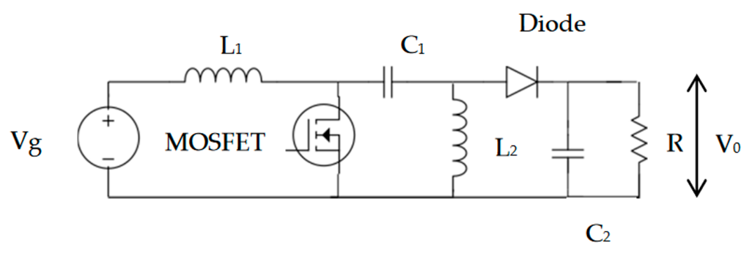
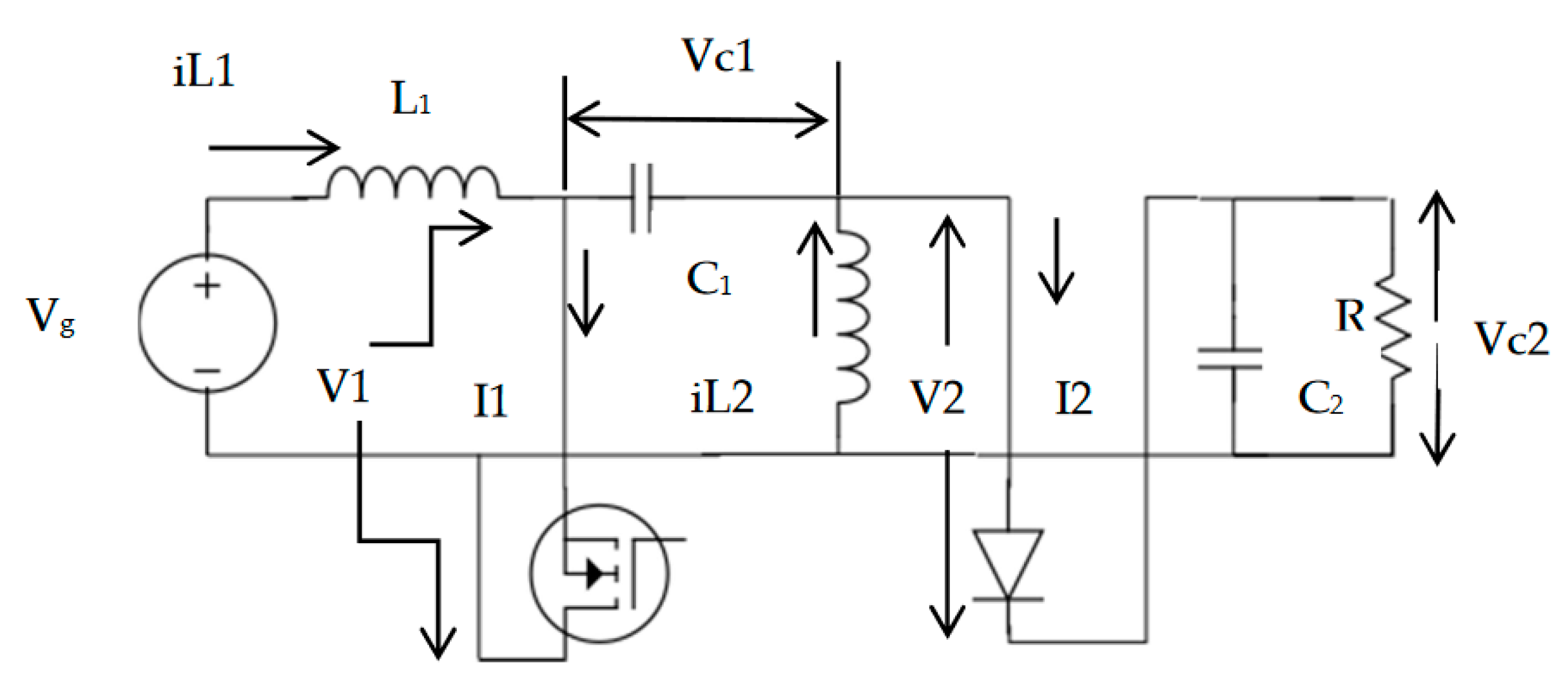
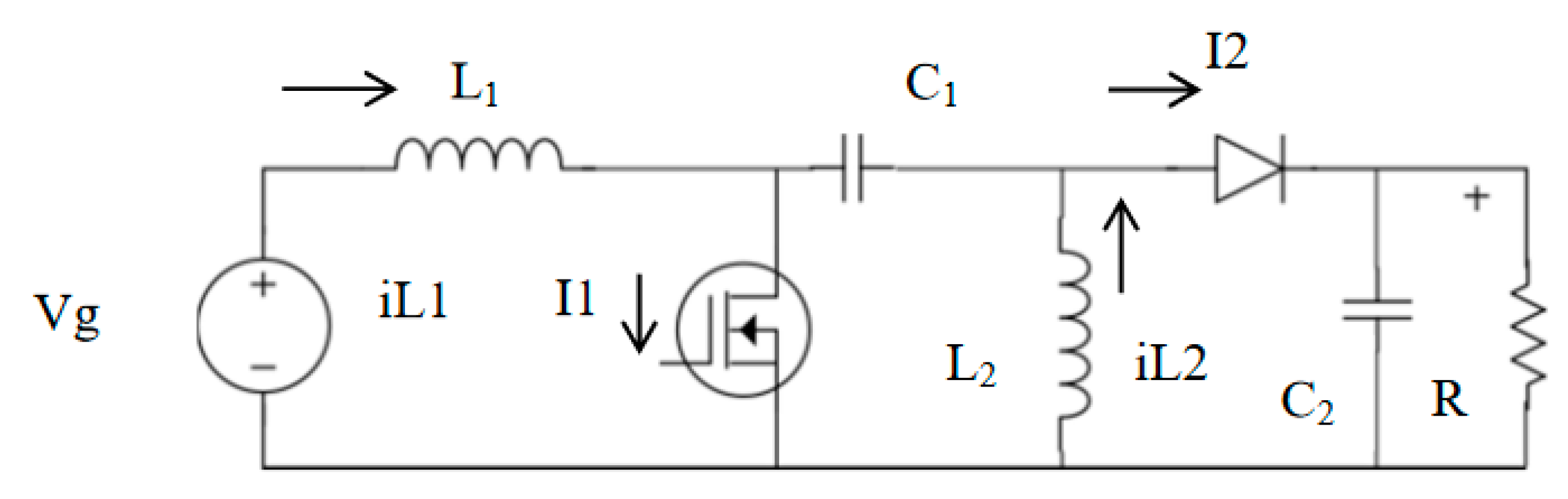
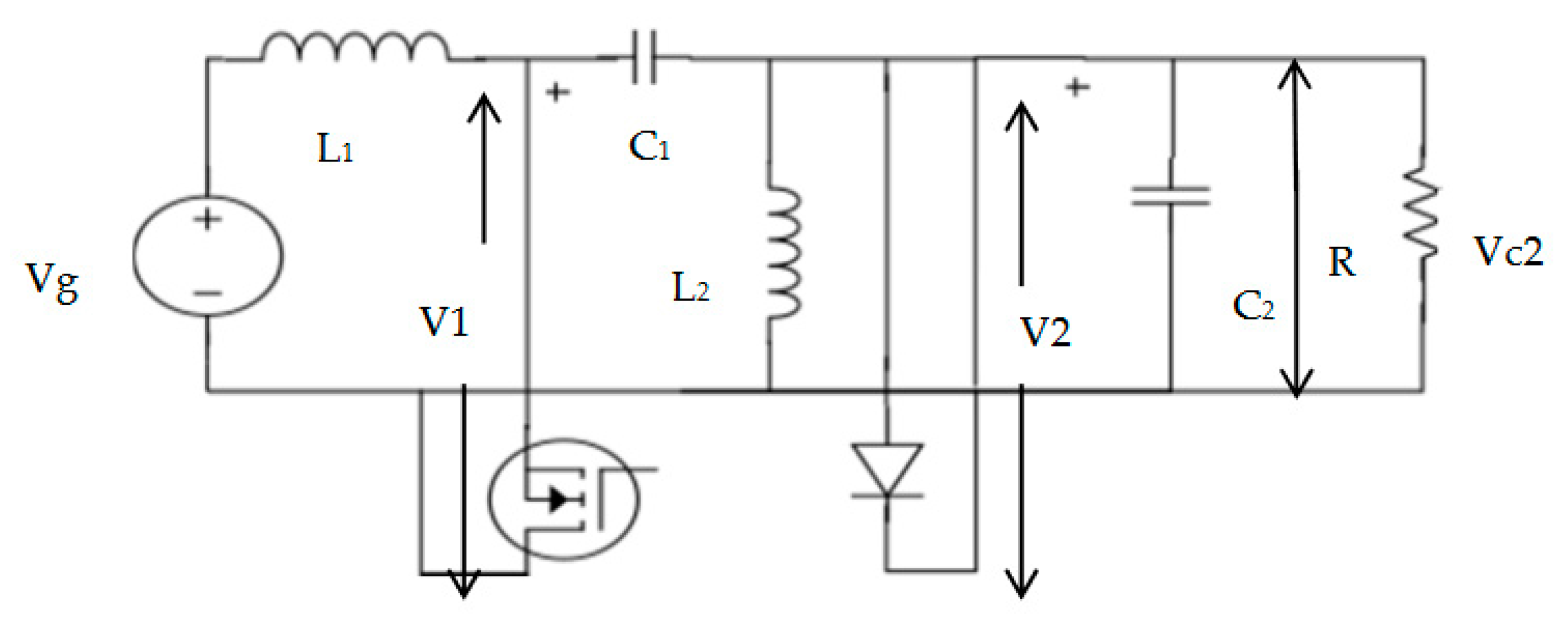
2. Circuit Averaging for an Ideal SEPIC

Figure 1 shows an ideal SEPIC with MOSFET and a diode. The voltages and currents are denoted as V1, V2, I1, and I2, respectively. Figure 2 shows the converter with the switches separated.
Circuit averaging of any converter involves three major steps viz.:
  • Separate the switch network from the converter and define the ports.
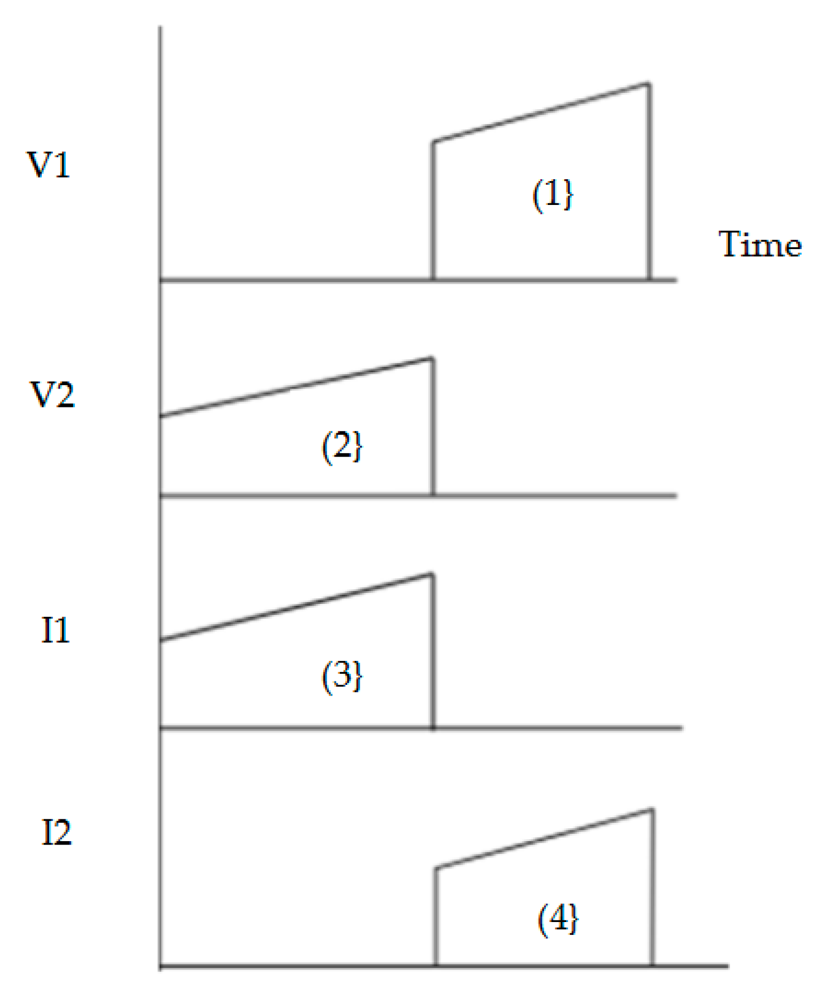
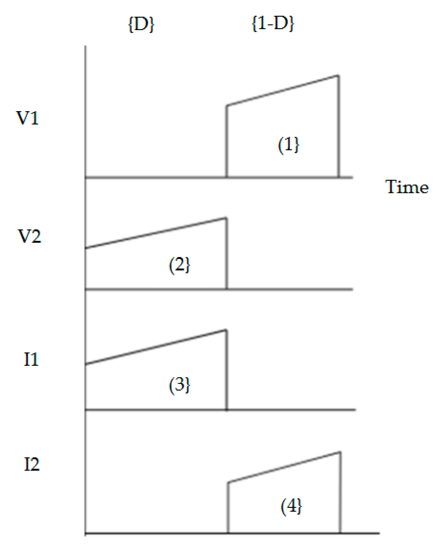
  • Sketch the waveform of the switch current and voltage waveforms and average it.
  • Simplify the equations and draw the equivalent switch network.
Averaging V1, V2, I1, and I2 waveforms:
V 1 = ( 1 d ) ( Vc 1 + Vc 2 )
V 2 = d ( Vc 1 + Vc 2 )
I 1 = d ( iL 1 + iL 2 )
I 2 = ( 1 d ) ( iL 1 + iL 2 )
From (1) and (2), eliminating (Vc1 + Vc2):
Vc 1 + Vc 2 = V 1 d = V 2 1 d
Vc 2 = V 1 d 1 d
Similarly, from (3) and (4), eliminating (iL1 + iL2):
I 1 = I 2 d 1 d
From (7) and (8), the turns ratio for the transformer can be derived as:
M = V 2 V 1 = N 2 N 1 = D 1 D
Equations (7) and (8) represent the generalized equations applicable to any switch PWM converter operating in CCM having two switches.

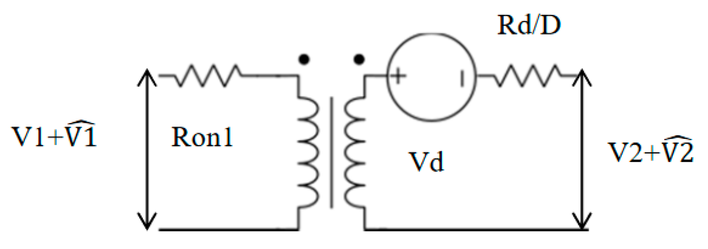
3. Small Signal Model

The small signal model provides the AC equivalent circuit in which the non-linear equations are linearized. V1, V2, I1, and I2 derived are now perturbed.
Perturbing (6):
( d d ^ ) ( V 2 + V 2 ^ ) = ( d + d ^ ) ( V 1 + V 1 ^ )
where d = 1 d .
Similarly, perturbing (7):
( d d ^ ) ( I 1 + I 1 ^ ) = ( d + d ^ ) ( I 2 + I 2 ^ )
Figure 3 shows the equivalent large signal DC/AC switch model.

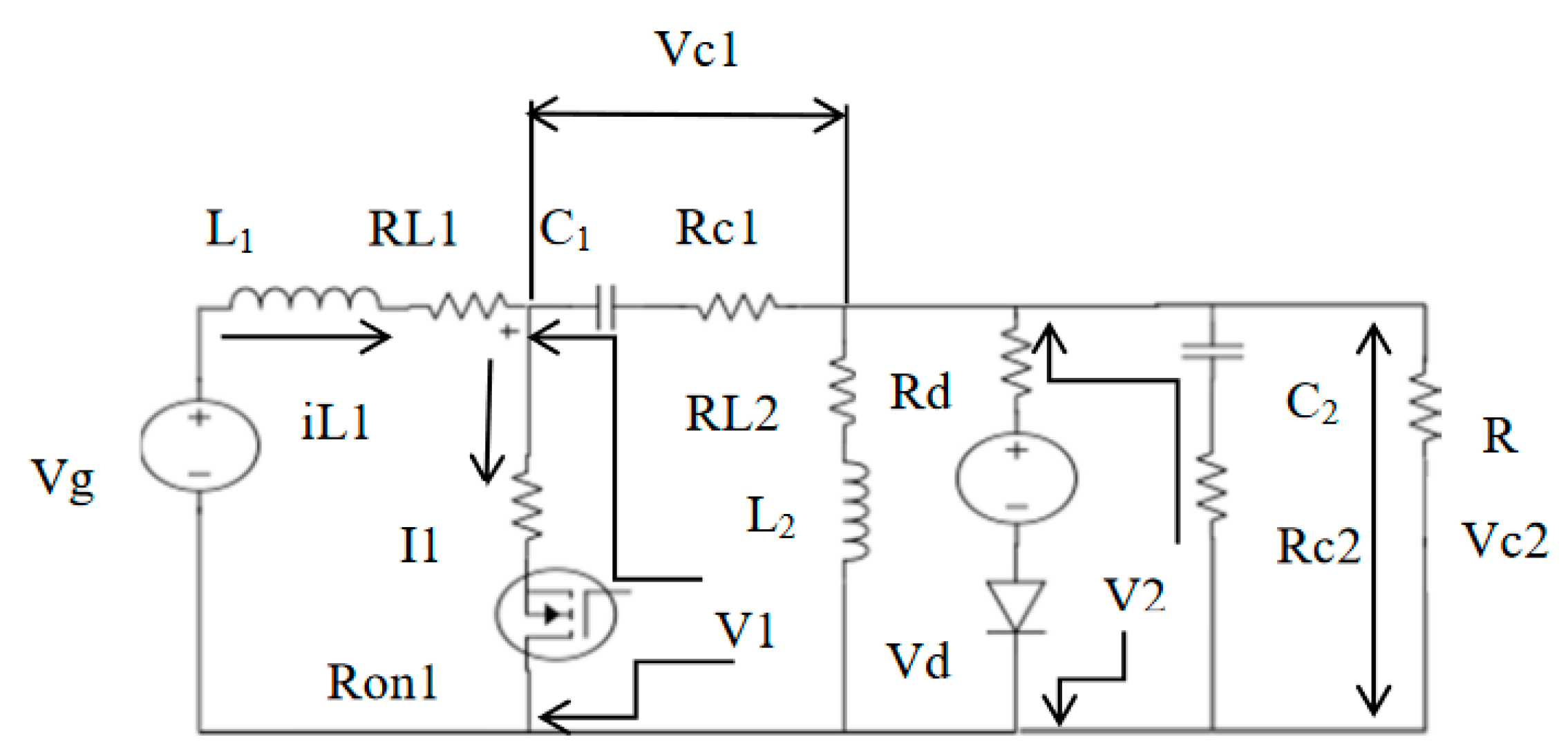
4. Circuit Averaging for a Non-Ideal SEPIC

Figure 4 shows the non-ideal SEPIC with V0 = Vc2.
V 1 = d ( Ron 1 ( iL 1 + iL 2 ) ) + d ( ( Vc 1 + Vc 2 ) + Vd + Rd ( iL 1 + iL 2 ) )
V 2 = d ( ( Vc 1 + Vc 2 ) Ron 1 ( iL 1 + iL 2 ) ) + d ( Vd + Rd ( iL 1 + iL 2 ) )
I 1 = d ( iL 1 + iL 2 )
I 2 = d ( iL 1 + iL 2 )
Simplifying (13) and (14):
I 1 d = I 2 1 d
From (12):
Vc 1 + Vc 2 = V 2 d + Ron 1 ( iL 1 + iL 2 ) d d ( Vd + Rd ( iL 1 + iL 2 ) )
Substituting (16) in (11) and upon simplification:
V 2 = I 1 Ron 1 d + ( 1 d d ) ( V 2 + Vd + Rd I 1 d )
The equivalent circuit for (18) is shown in Figure 5.

5. Circuit Averaging for a Non-Ideal Cuk

Figure 6 shows an ideal Cuk converter operating in CCM. Figure 7 shows the MOSFET and diode separated from the converter.
Figure 8 shows the waveforms of switch voltages and currents at dTs and (1 − d)Ts intervals, which is similar to Figure 9.
V 1 = Vc 1 ( 1 d )
V 2 = dVc 1
I 1 = d ( iL 1 + iL 2 )
I 2 = ( 1 d ) ( iL 1 + iL 2 )
Eliminating Vc1:
V 1 1 d = V 2 d
V 2 = ( V 1 d ) / d
The turns ratio of the transformer irrespective of the converter would remain the same, i.e.:
M = N 2 N 1 = V 2 V 1 = D 1 D
Therefore, the equivalent circuit would remain the same as that of the SEPIC.

6. Circuit Averaging for Non-Ideal Cuk Converter

On averaging the voltages and currents across the switches:
V 1 = d ( Ron 1 ( iL 1 + iL 2 ) ) + d ( Vc 1 + Vd + Rd ( iL 1 + iL 2 ) )
V 2 = d ( Vc 1 Ron 1 ( iL 1 + iL 2 ) ) d ( Vd + Rd ( iL 1 + iL 2 ) )
I 1 = d ( iL 1 + iL 2 )
I 2 = d ( iL 1 + iL 2 )
Eliminating iL1 and iL2:
I 1 d = I 2 d
From (25):
Vc 1 = V 2 d Ron 1 I 1 d + 1 d d ( Vd + Rd I 1 d )
Substituting (29) in (24):
V 1 = I 1 Ron 1 d + 1 d d ( Vd + Rd I 1 d )
The small signal is generic and provides results for any DC-DC converter having two switches operating in CCM.

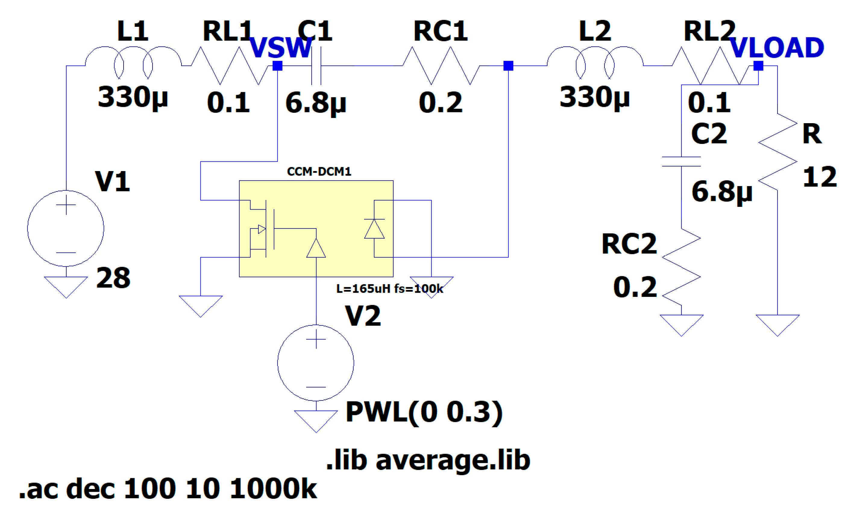
7. Converter Specifications
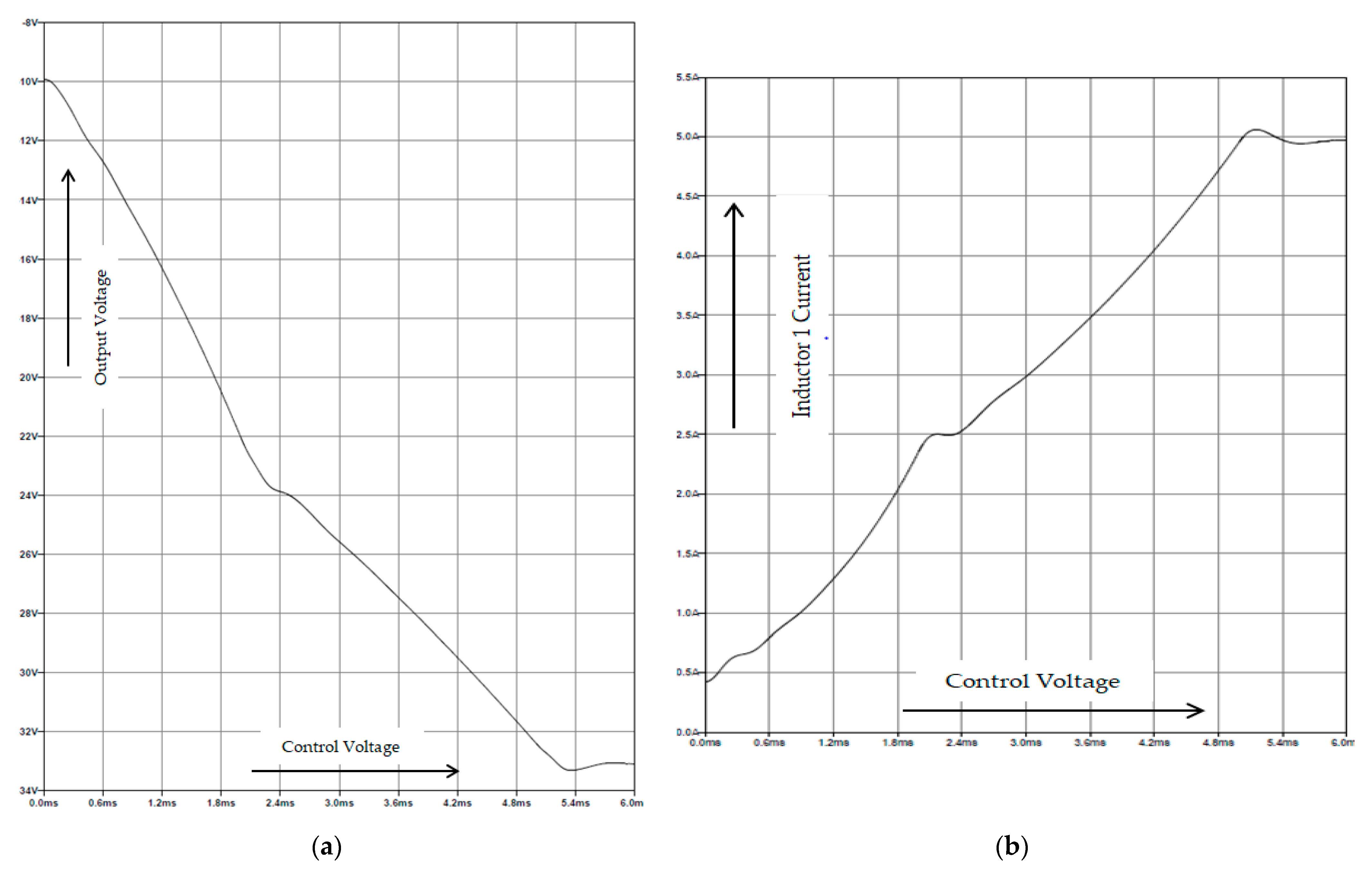
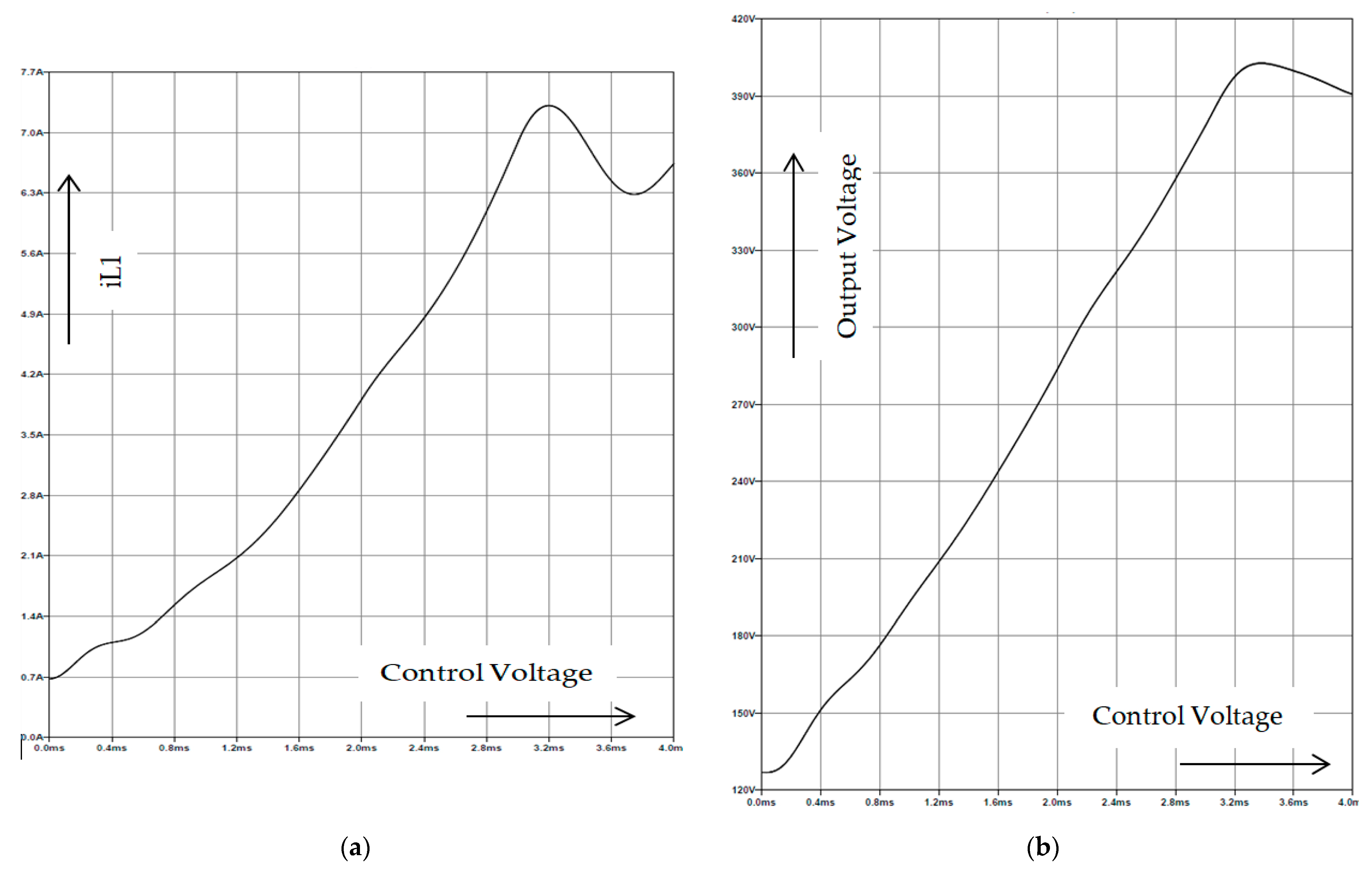
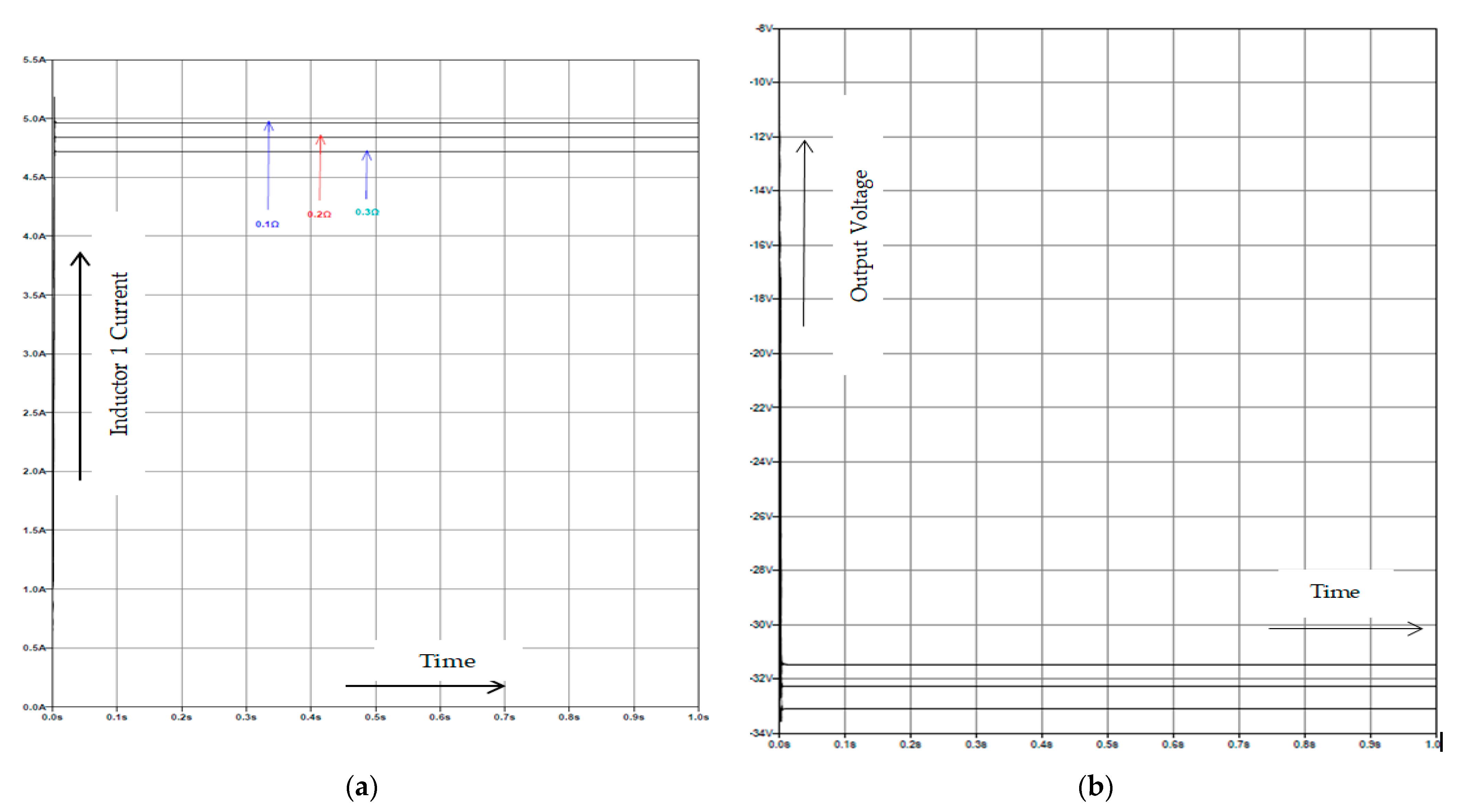
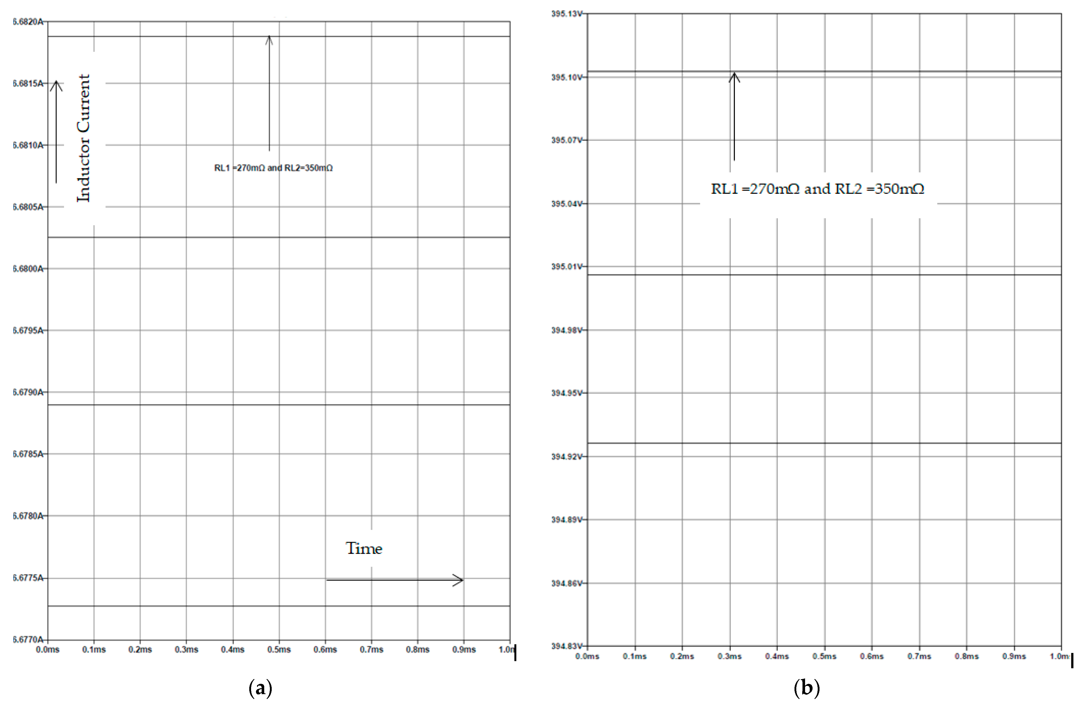
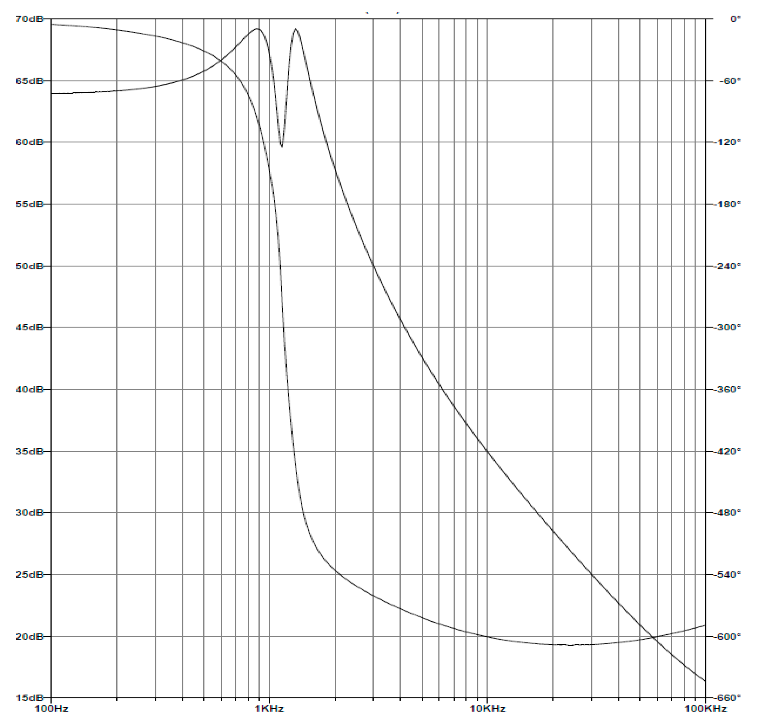
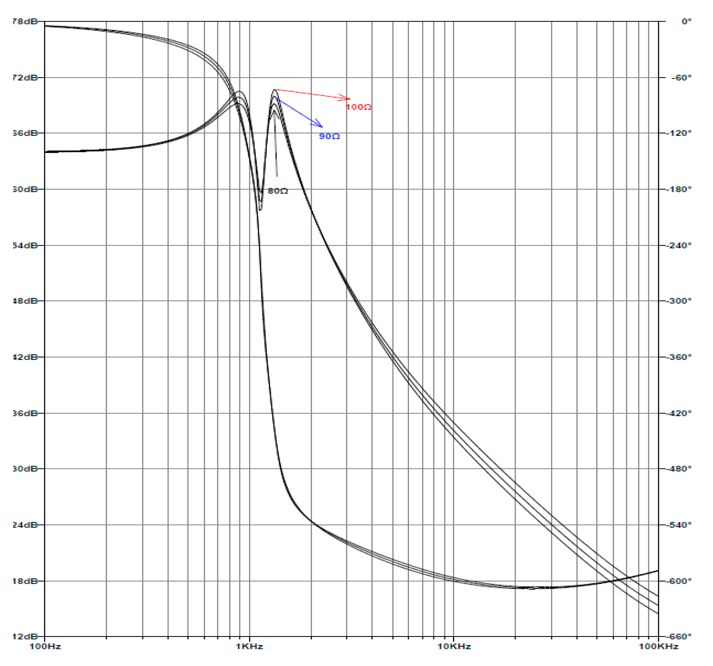
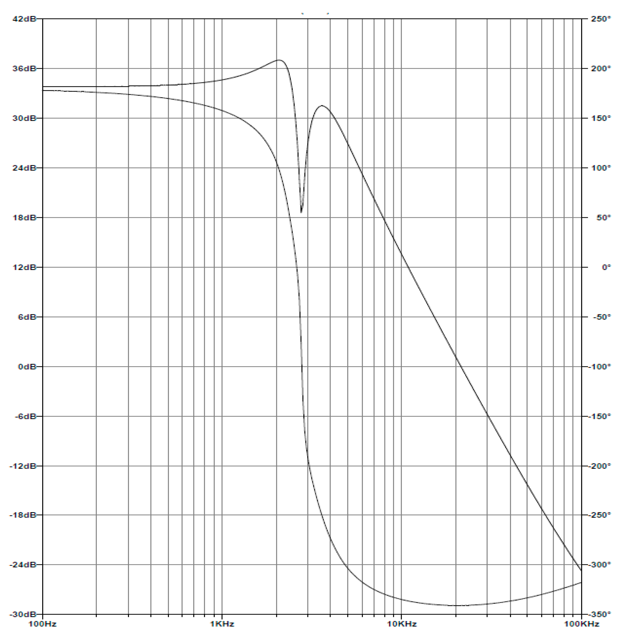
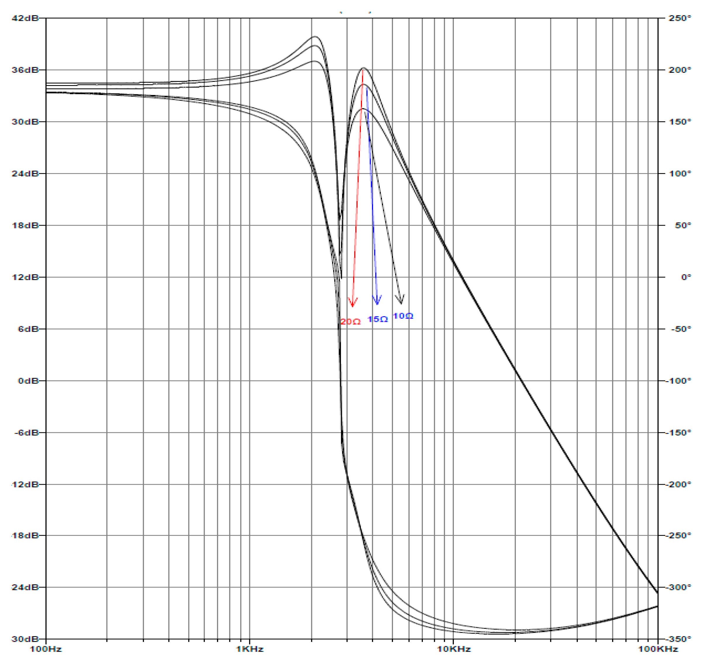
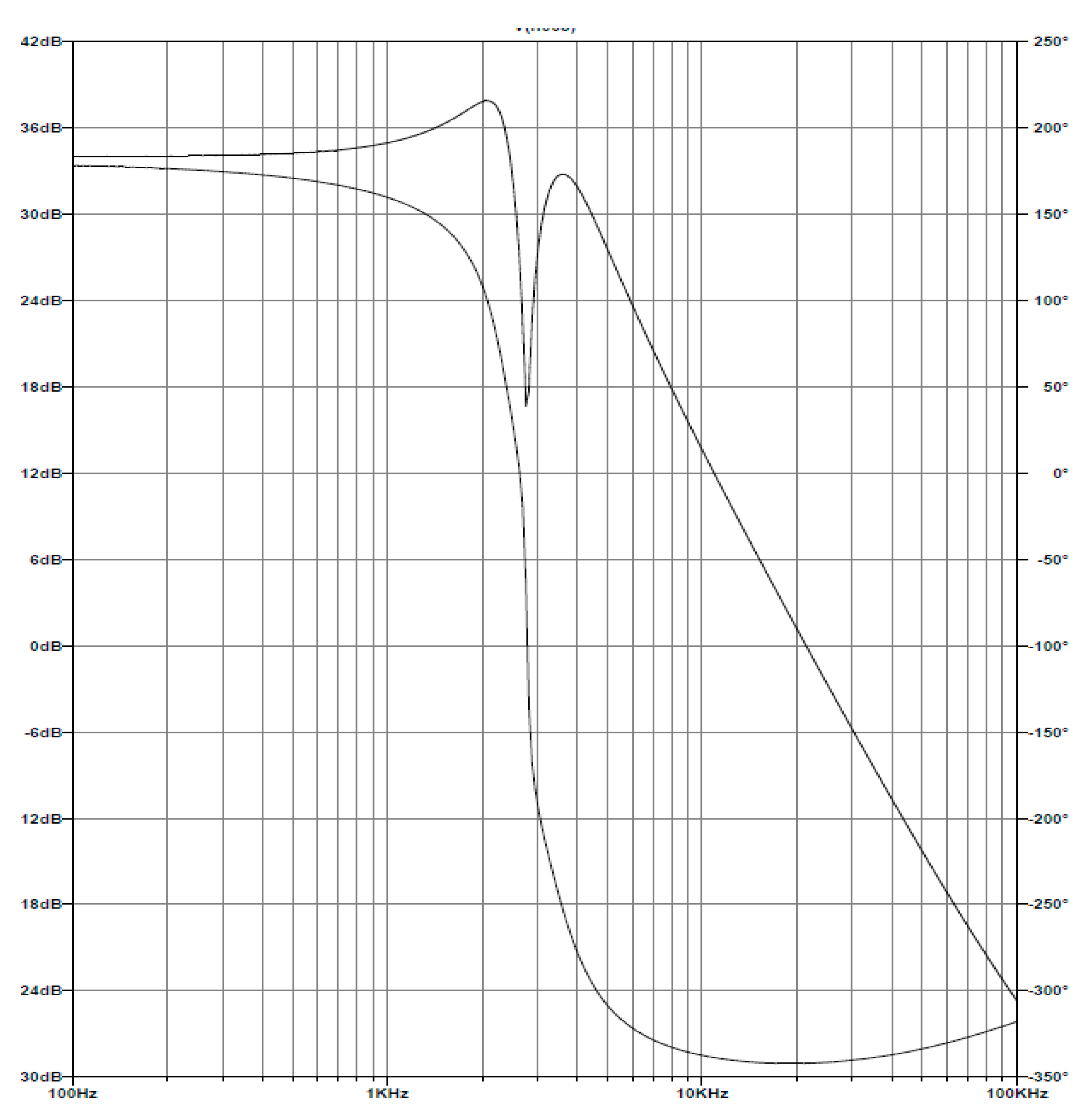
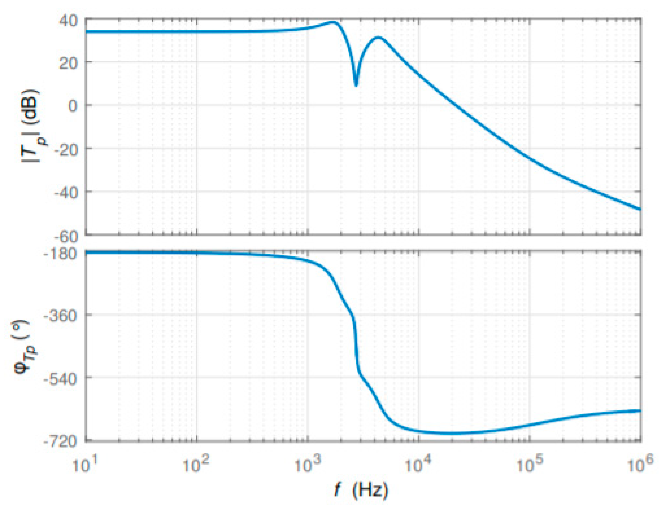
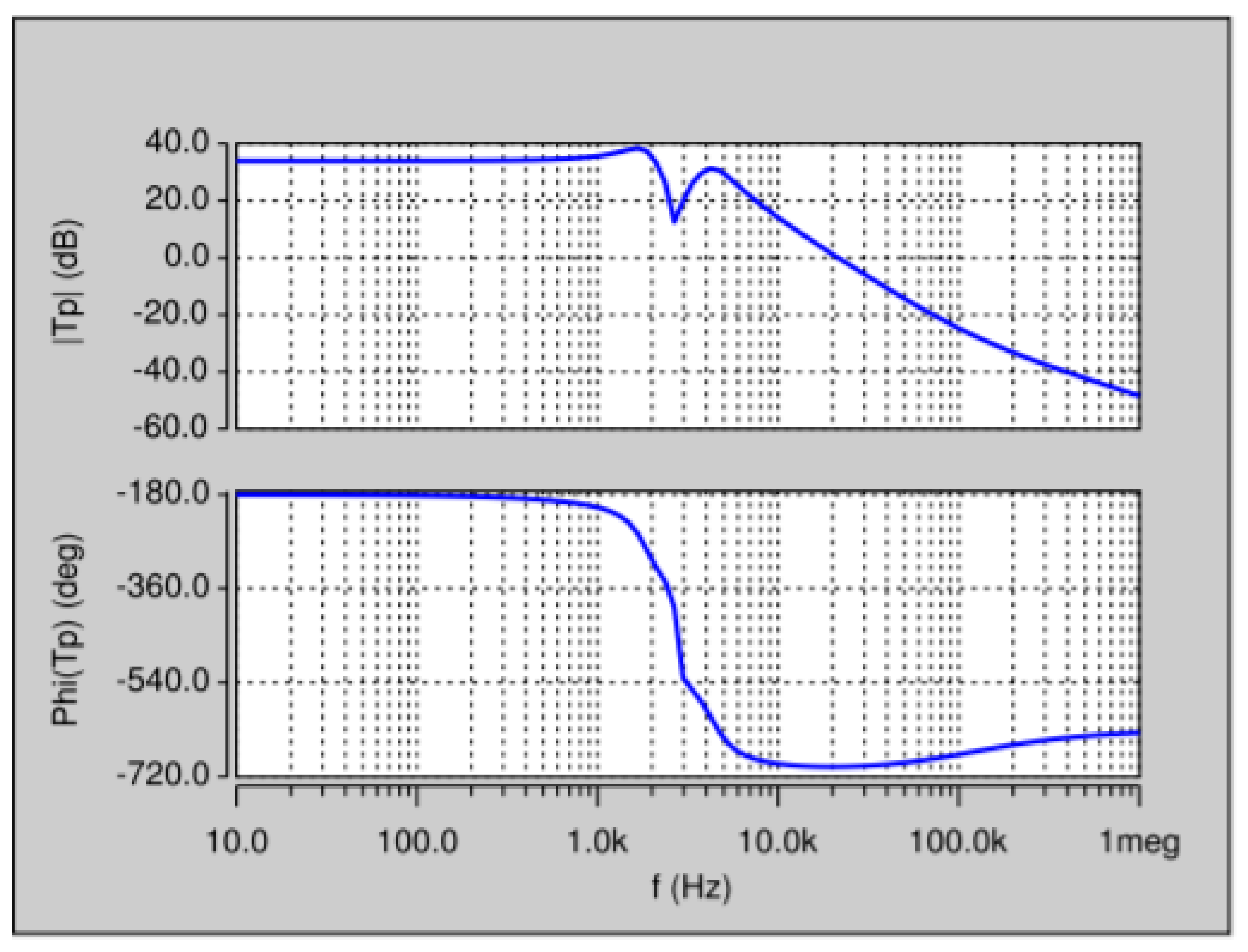
Table 1 shows the specifications of Non-ideal Cuk converter.
Table 2 shows the specifications of Non-ideal SEPIC.

8. Results

Simulations were performed using LTSpice software. The equivalent switch network was available as a built-in library under ‘average.lib’ library.
D was varied from 0.3 to 0.6 every 1 ms and the corresponding iL1 and V0 were analyzed. Figure 10 and Figure 11 show the variation of iL1 and V0 with respect to the D for Cuk and SEPIC, respectively. It was observed that an increase in D caused an increase in iL1. However, V0 for Cuk and SEPIC increased in the negative and positive directions, respectively.
In Figure 12, RL was varied from 0.1 Ω to 0.3 Ω in steps of 0.1. It was observed that higher RL provided higher iL1 and V0. SEPIC also showed similar features. In Figure 13, RL1 and RL2 were varied. It was found that the lowest value of RL1 and the highest value of RL2 provided higher voltage levels.
Figure 14 shows the Bode plot of Gvd for an SEPIC under the variation of D from 0.2 to 0.9 in steps of 0.01 considering a fixed load. The crossover frequency was about 4.207 kHz, gain cross over frequency about 169.45 kHz, gain margin about −43.60 dB, and phase margin about −30°. Thus, the open loop behavior of SEPIC is unstable. A step change in R varying from 80 Ω to 100 Ω in steps of 10 Ω was simulated. As shown from Figure 15, a higher value of R created higher resonance.
Similar to that of SEPIC, D was varied from 0.2 to 0.9 in steps of 0.01 for a non-ideal Cuk converter. The cross-over frequency was about 2.92 kHz with a gain margin and phase margin of about −23.85 dB and −160.894°, respectively. Thus, the open-loop system was unstable. Figure 16 shows a bode plot of Gvd for a fixed value of R. A similar feature in Gvd for varying R was seen in the practical Cuk converter shown in Figure 17. Gvd was computed in LTSpice software using the AC sweep command.
The frequency response of Gvd obtained from the circuit averaging and small signal model for a non-ideal Cuk converter was compared. The specifications shown in [3] were chosen, simulated, and compared. Figure 18 shows the circuit averaging model for the selected converter using the LTSpice software tool. Figure 19 shows Gvd obtained from the circuit averaging technique using the AC sweep command. Figure 20 and Figure 21 show the Gvd plots based on [3].
It can be observed that Gvd obtained from circuit averaging and [4] closely match.

9. Conclusions

The circuit averaging technique for fourth-order converters like Cuk and SEPIC was carried out using the LTSpice software tool. This generalized approach to predict the frequency response of Gvd can be applied for any two-switch PWM DC-DC converters operating in CCM. This method is comparatively simple and easy to implement compared to the conventional small signal and state space averaged models. The lowest value of RL1 and the highest value of RL2 cause higher voltage levels. Gvd becomes unstable in the open-loop configuration for the chosen converters. This technique does not provide the transfer function equation of Gvd. However, the specifications like gain and phase margins and gain and phase cross-over frequencies can be easily found and its stability can be analyzed. The LTSpice model was used for the two-switch configuration in this paper. However, it can be extended to converters having multiple switches.

Author Contributions

Proposed idea and carried out modeling and simulation, S.S.; Guidance and Advice, S.W. Both authors have read and agreed to the published version of the manuscript.

Funding

This research received no external funding.

Institutional Review Board Statement

Not applicable.

Informed Consent Statement

Not applicable.

Data Availability Statement

Not applicable.

Conflicts of Interest

The authors declare no conflict of interest.

References

  1. Erickson, W.R.; Maksimovic, D. Fundamentals of Power Electronics; Springer Science & Business Media: Berlin/Heidelberg, Germany, 2007. [Google Scholar]
  2. Surya, S.; Patil, V. Cuk Converter as an Efficient Driver for LED. In Proceedings of the 2019 4th International Conference on Electrical, Electronics, Communication, Computer Technologies and Optimization Techniques (ICEECCOT), Mysuru, India, 13–14 December 2019. [Google Scholar]
  3. Surya, S.; Arjun, M.N. Effect of fast discharge of a battery on its core temperature. In Proceedings of the 2020 International Conference on Futuristic Technologies in Control Systems & Renewable Energy (ICFCR), Malappuram, India, 23–24 September 2020. [Google Scholar]
  4. Kathi, L.; Ayachit, A.; Saini, D.K.; Chadha, A.; Kazimierczuk, M.K. Open-loop small-signal modeling of Cuk DC-DC converter in CCM by circuit-averaging technique. In Proceedings of the 2018 IEEE Texas Power and Energy Conference (TPEC), College Station, TX, USA, 8–9 February 2018. [Google Scholar]
  5. Lee, C.M.; Lai, Y.S. Averaged switch modeling of dc/dc converters using new switch network. In Proceedings of the 2007 7th International Conference on Power Electronics and Drive Systems, Bangkok, Thailand, 27–30 November 2007. [Google Scholar]
  6. Middlebrook, R.D.; Cuk, S. A General Unified Approach to Modeling Switching Converter Stages. In Proceedings of the 1976 IEEE Power Electronics Specialists Conference, Cleveland, OH, USA, 8–10 June 1976; pp. 18–34. [Google Scholar]
  7. Niculescu, E.; Iancu, E.P. Modeling and analysis of the DC/DC fourth-order PWM converters. In Proceedings of the COMPEL 2000, 7th Workshop on Computers in Power Electronics, Proceedings (Cat. No. 00TH8535), Blacksburg, VA, USA, 16–18 July 2000. [Google Scholar]
  8. Van Dijk, E.; Spruijt, J.N.; O’sullivan, D.M.; Klaassens, J.B. PWM-switch modeling of DC-DC converters. IEEE Trans. Power Electron. 1995, 10, 659–665. [Google Scholar] [CrossRef] [Green Version]
  9. Sumukh, S.; Channegowda, J.; Naraharisetti, K. Generalized Circuit Averaging Technique for Two Switch DC-DC Converters. arXiv 2020, arXiv:2012.12724. [Google Scholar]
  10. Ayachit, A.; Kazimierczuk, M.K. Averaged small-signal model of PWM DC-DC converters in CCM including switching power loss. IEEE Trans. Circuits Syst. II Express Briefs 2018, 66, 262–266. [Google Scholar] [CrossRef]
  11. Bertoldi, B.; Junior, M.M.B.; Dall’Asta, M.S.; Mocellini, M.P.; Roig, G.M.D.; Kirsten, A.L.; Heldwein, M.L. A Non-Ideal SEPIC DCM Modeling for LED Lighting Applications. In Proceedings of the 2018 IEEE 4th Southern Power Electronics Conference (SPEC), Singapore, 10–13 December 2018. [Google Scholar]
  12. Simonetti, D.S.L.; Sebastian, J.; Uceda, J. The discontinuous conduction mode Sepic and Cuk power factor preregulators: Analysis and design. IEEE Trans. Ind. Electron. 1997, 44, 630–637. [Google Scholar] [CrossRef] [Green Version]
  13. Singer, S.; Erickson, R.W. Canonical modeling of power processing circuits based on the POPI concept. IEEE Trans. Power Electron. 1992, 7, 37–43. [Google Scholar] [CrossRef]
Figure 1. Circuit diagram.
Electronics 10 00392 g001
Figure 2. Separate the switches.
Electronics 10 00392 g002
Figure 3. Equivalent switch network, where {1} is d ^ V 1 d d and {2} is I 2 d ^ d d .
Electronics 10 00392 g003
Figure 4. Switches separated.
Electronics 10 00392 g004
Figure 5. Equivalent switch circuit.
Electronics 10 00392 g005
Figure 6. Circuit diagram.
Electronics 10 00392 g006
Figure 7. Switches separated.
Electronics 10 00392 g007
Figure 8. Waveforms during switch ON and OFF conditions.
Electronics 10 00392 g008
Figure 9. Waveforms during Switch ON and OFF conditions, where {1} and {2} are Vc1 + Vc2 and {3} and {4} are iL1 + iL2.
Electronics 10 00392 g009
Figure 10. Variation of iL1 and V0 with change in D (Cuk). (a) Output Voltage Vs. Control Voltage, (b) Inductor 1 Current Vs. Control Voltage
Electronics 10 00392 g010
Figure 11. Variation of iL1 and V0 with change in D (SEPIC). (a) Output Voltage Vs. Control Voltage, (b) Inductor 1 Current Vs. Control Voltage
Electronics 10 00392 g011
Figure 12. Variation of iL1 and V0 with change in RL (Cuk). (a) Output Voltage Vs. Control Voltage, (b) Inductor 1 Current Vs. Control Voltage
Electronics 10 00392 g012
Figure 13. Variation of iL1 and V0 with change in RL (SEPIC). (a) Output Voltage Vs. Control Voltage, (b) Inductor 1 Current Vs. Control Voltage
Electronics 10 00392 g013
Figure 14. Gvd for SEPIC for fixed R.
Electronics 10 00392 g014
Figure 15. Gvd for SEPIC for variable R.
Electronics 10 00392 g015
Figure 16. Gvd for Cuk for variable R.
Electronics 10 00392 g016
Figure 17. Gvd for Cuk for variable R.
Electronics 10 00392 g017
Figure 18. Circuit averaged model.
Electronics 10 00392 g018
Figure 19. Gvd for a non-ideal Cuk converter.
Electronics 10 00392 g019
Figure 20. Theoretically derived Gvd for a non-ideal Cuk converter [4].
Electronics 10 00392 g020
Figure 21. MATLAB-generated Gvd for a non-ideal Cuk converter [4].
Electronics 10 00392 g021
Table 1. Specifications of non-ideal Cuk.
SL.NOSpecificationsValue
1Input Voltage, Vg28 V
2Output Voltage, V010 V
3Output Current, I01 A
4Inductors, L1 and L2330 µH
5Inductor ESR, RL1 and RL20.1 Ω
6MOSFET Resistance, Ron131 mΩ
7Duty Cycle, D0.3
8Capacitors, C1 and C26.8 µH
9Capacitor ESR, Resr0.2 Ω
10Switching Frequency, fs100 kHz
11Diode Drop, Vd0.8 V
12Diode Forward Resistance0.8 Ω
Table 2. Specifications of non-ideal SEPIC.
SL.NOSpecificationsValue
1Input Voltage, Vg300 V
2Output Voltage, V0400 V
3Output Current, I05 A
4Inductors, L1 and L22.57 mH & 1.71 mH
5Inductor ESR, RL1 and RL2130 mΩ & 110 mΩ
6MOSFET Resistance, Ron1321 mΩ
7Duty Cycle, D0.571
8Capacitors, C1 and C24.7 µF & 3.57 µF
9Capacitor ESR, Resr270 mΩ & 350 mΩ
10Switching Frequency, fs100 kHz
11Diode Drop, Vd0.62 V
12Diode Forward Resistance80 mΩ
Publisher’s Note: MDPI stays neutral with regard to jurisdictional claims in published maps and institutional affiliations.

