Article

The Analysis of SEU in Nanowire FETs and Nanosheet FETs

1
Department of Electronics Engineering, Korea National University of Transportation, Room No. 326, Smart ICT Building, 50 Daehak-ro, Chungju-si, Chungbuk 27469, Korea
2
Department of IT and Energy Convergence (BK21 FOUR), Korea National University of Transportation, Room. 326, ICT Building, 50 Daehak-ro, Chungju-si, Chungbuk 27469, Korea
*
Author to whom correspondence should be addressed.
Electronics 2021, 10(7), 863; https://doi.org/10.3390/electronics10070863
Submission received: 2 March 2021 / Revised: 30 March 2021 / Accepted: 2 April 2021 / Published: 5 April 2021
(This article belongs to the Special Issue New CMOS Devices and Their Applications II)

Abstract

:
The effects of the single-event upset (SEU) generated by radiation on nanowire field-effect transistors (NW-FETs) and nanosheet (NS)-FETs were analyzed according to the incident angle and location of radiation, by using three-dimensional technology computer-aided design tools. The greatest SEU occurred when the particle was incident at 90°, whereas the least occurred at 15°. SEU was significantly affected when the particle was incident on the drain, as compared to when it was incident on the source. The NS-FETs were robust to SEU, unlike the NW-FETs. This phenomenon can be attributed to the difference in the area exposed to radiation, even if the channel widths of these devices were identical.

1. Introduction

When high-energy radiation is incident on semiconductor circuits, many electron–hole pairs (EHPs) are generated. These generated EHPs extend the depletion layer and move into the drain. This causes electrical noise, and the phenomenon is called the “single-event effect” (SEE) [1,2,3]. Single-event upset (SEU) is a type of SEE that flips stored data. This can be resolved through a device reboot or data rewriting. However, in devices such as very-large-scale integration (VLSI) devices, small flip-flop errors can cause critical issues [4,5,6,7].
There are limitations in measuring the SEU in environments involving space radiation [8,9]. As most radiation effects dissipate rapidly, removing the device from the environment involving radiation affords significant recovery. Consequently, radiation effects are evaluated through simulations [10,11,12]. This work aims to compare the SEU in nanowire field-effect transistors (NW-FETs) and nanosheet (NS)-FETs. As technology develops and devices shrink, three-dimensional (3D) FETs frequently require improved gate controllability and a reduction in short-channel effects [13,14]. Although FinFETs are frequently used, NW-FETs and NS-FETs have the potential to replace FinFET devices [15,16]. As NW-FETs and NS-FETs have different channel structures, the effects of SEU on different radiation-exposed areas were compared. In addition, in a radiation environment, radiation is not incident in a certain direction alone; it follows various trajectories. Hence, it is necessary to determine and understand the cases wherein the strongest effects occur. SEU is affected by the incident angle and location of the radiation [17,18]. Therefore, in this study, the effect of these parameters on the SEU in NW-FETs and NS-FETs was analyzed in detail.

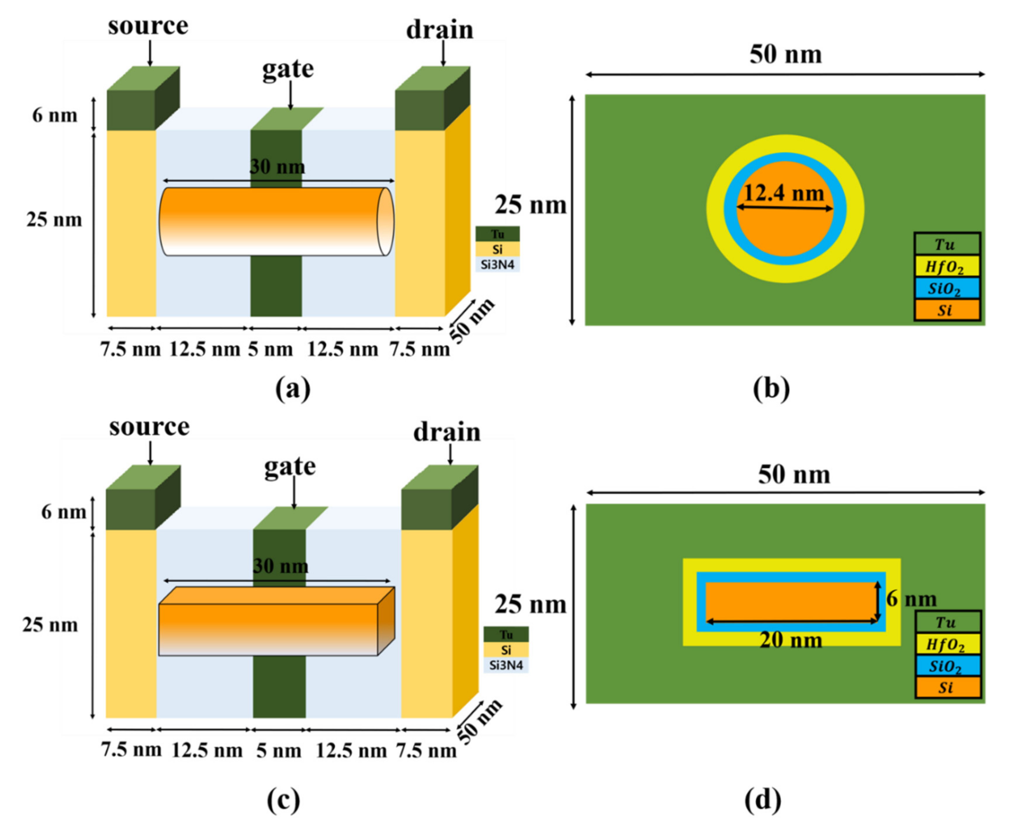
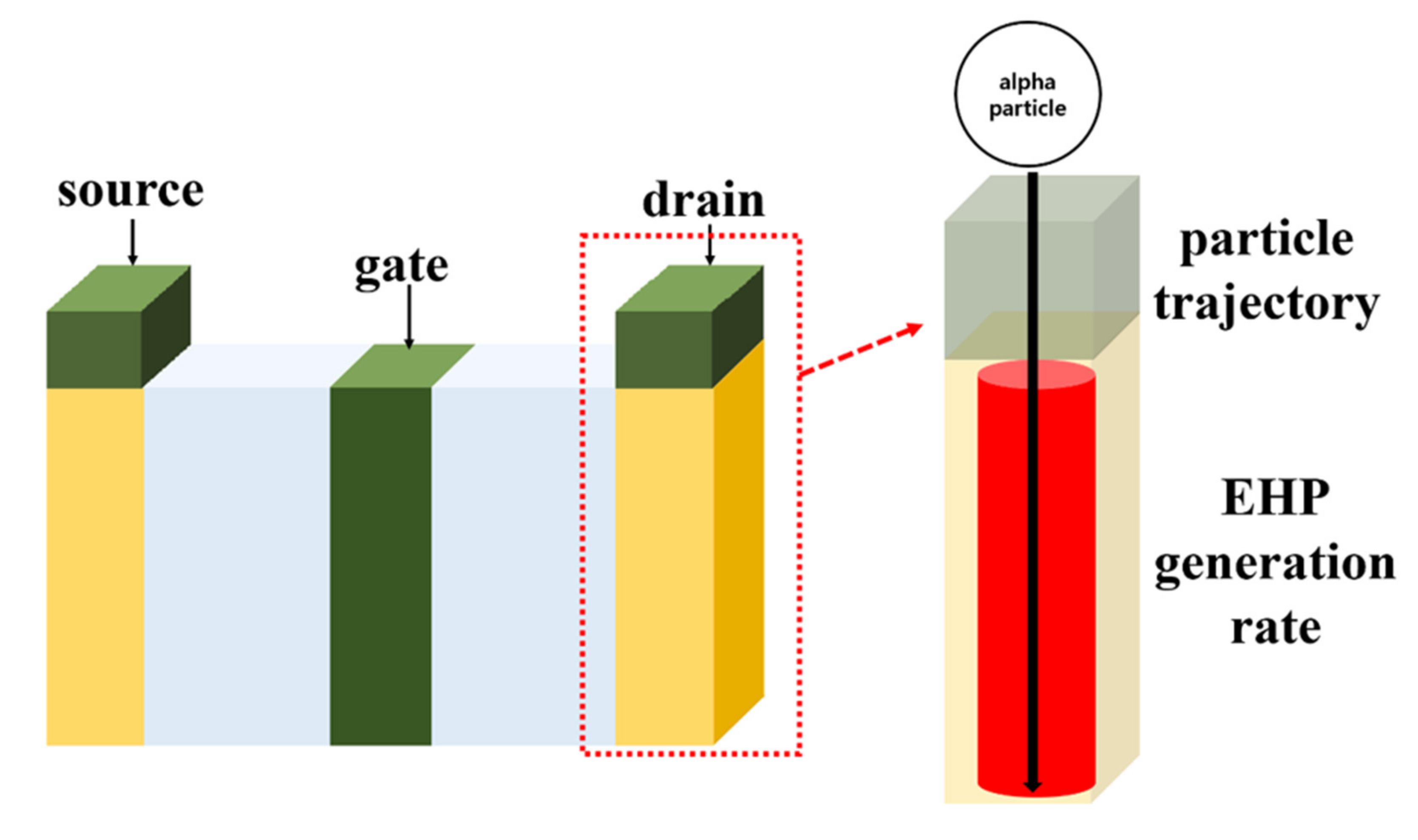
2. Proposed Structure and Operation
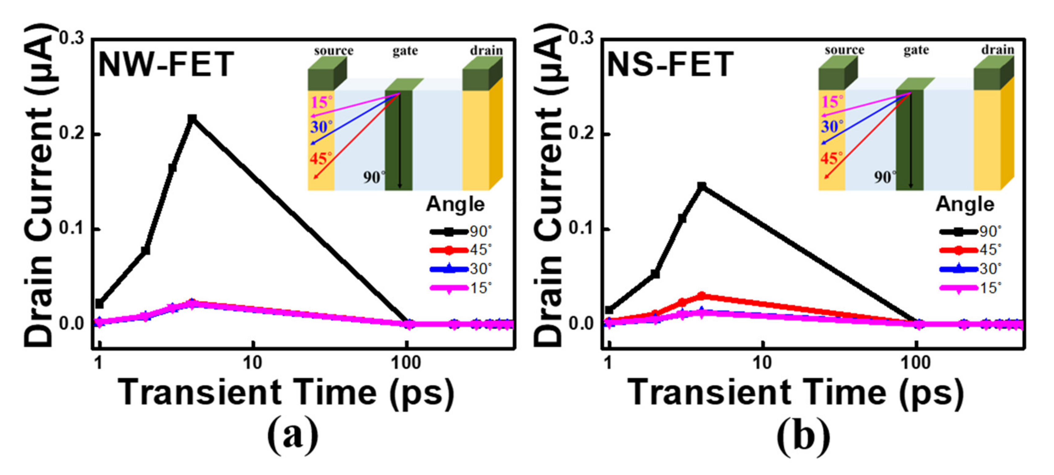
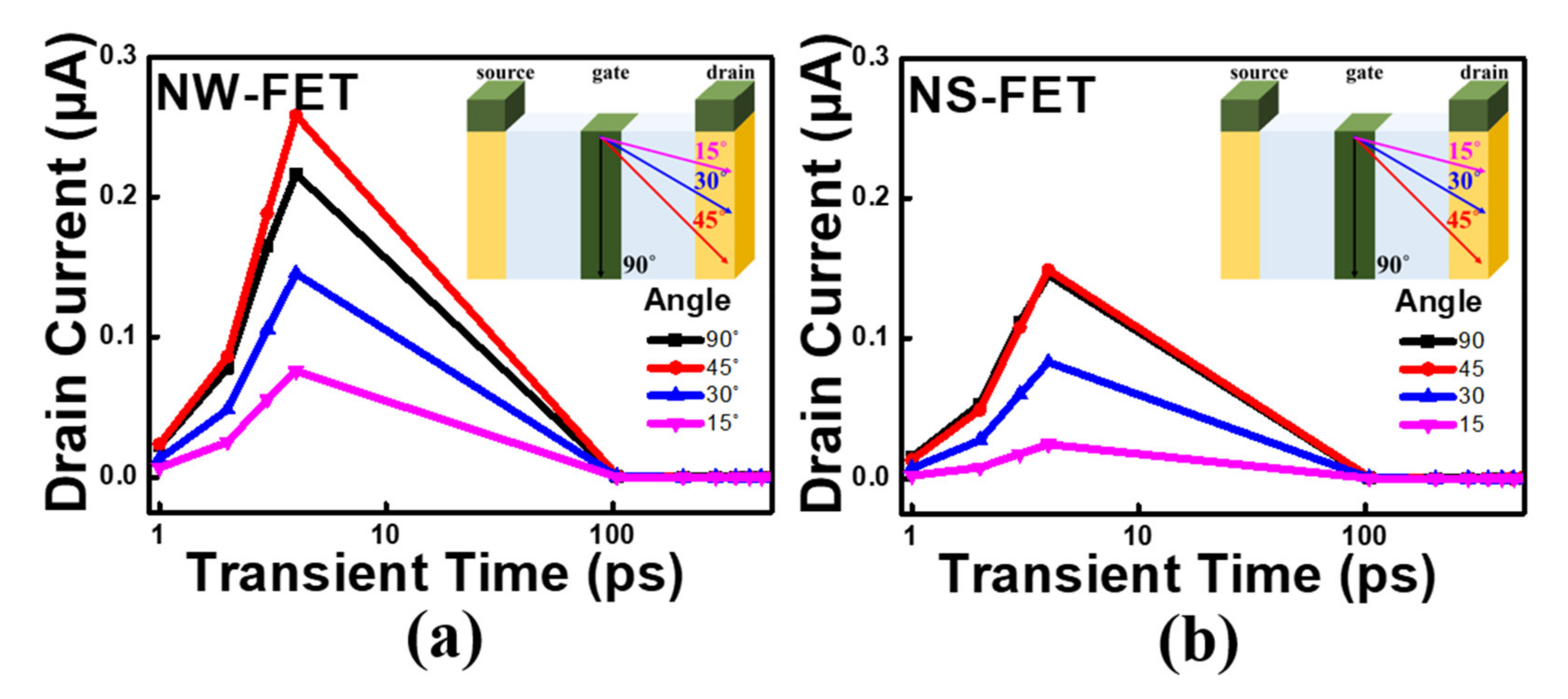
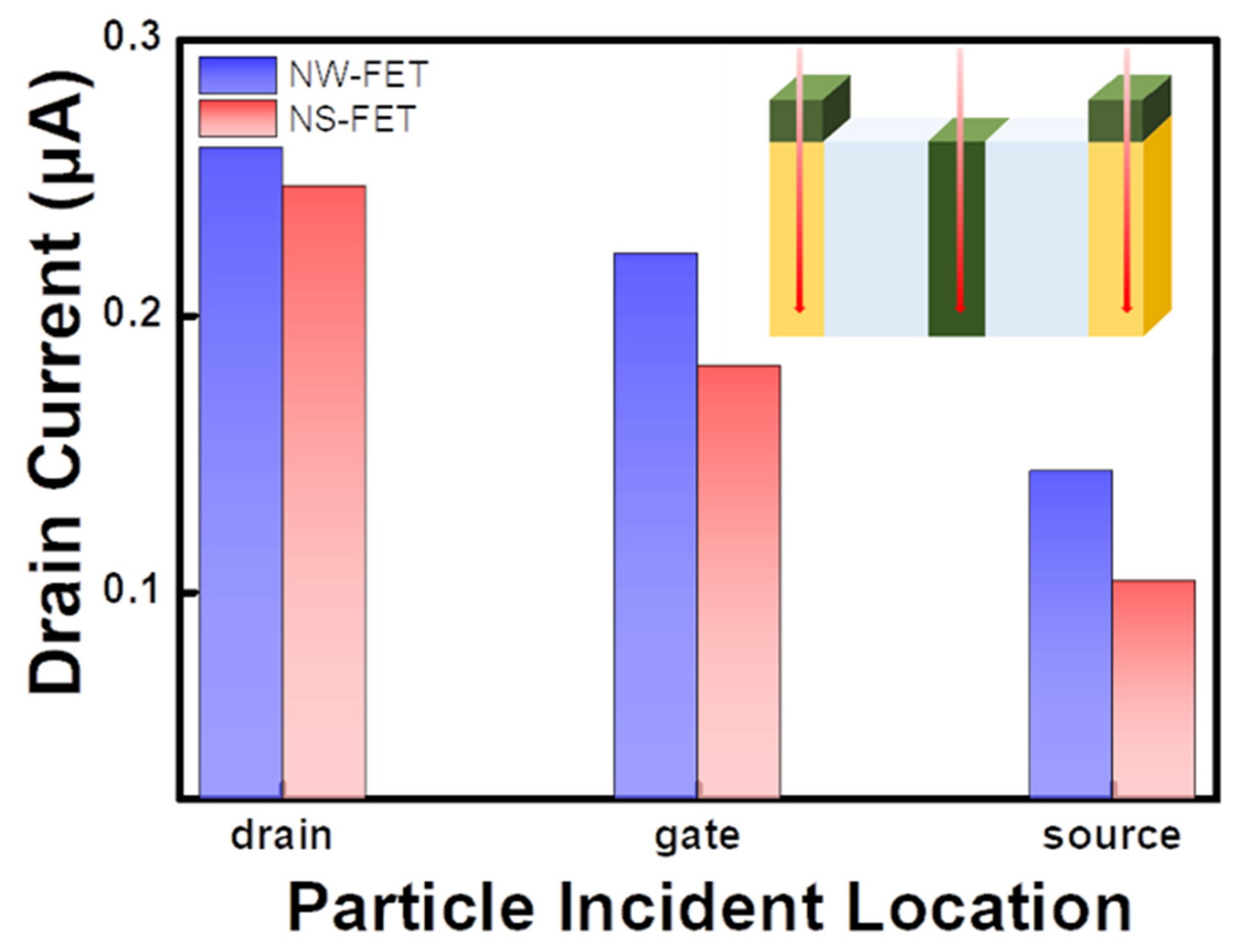
Figure 1a,c show the external structures of the NW-FET and NS-FET used in 3D technology computer-aided design (TCAD) tools. Figure 1b,d show the cross-sections of the NW-FET and NS-FET. Both devices had the same external specifications. Table 1 lists the specifications of the NW-FET and NS-FET.
Figure 2 explains the SEU generation in the device, simulated using the Silvaco ATLAS tool. As shown in Figure 2, the SEU phenomenon can be observed when radiation is incident on the drain. An alpha particle was used in simulation. The trajectory of the incident radiation was set based on the coordinates of the start and end points of the radiation. In each simulation, the coordinates of the radiation incident on the device were matched, and the incident angle was adjusted by changing the endpoint of the coordinates. As the radiation was instantaneously incident and temporarily added noise, the time period within which the radiation is incident was set. Before the radiation was incident, the drain voltage was set to 0.5 V, the radiation radius was set to 5 nm, and the density was set to 1 × 1019 cm3. Radius is a criterion that controls the radius of the trajectory, and density is a criterion that controls the amount of incident radiation.

3. Results

Figure 3 shows the change in the drain current over time when radiation was incident on each drain at 90°, 45°, 30°, and 15° toward the source. When the particle incident on each device was incident at 90° relative to the drain, the drain current exhibited the most significant change. As the incident angle decreased, the amount of drain current decreased. If the particle incident was near the drain, generated electrons could move quickly into the drain. They caused more SEU effects on devices. In addition, a comparison of the two devices showed that the drain current of the NW-FET changed more than that of the NS-FET.
Figure 4 shows the change in the drain current when the particle struck through the gate to the source. The drain current changed most when the particle was incident at 90°, whereas at the other angles, there was negligible change. This is because the particle incident trajectory that generated the EHP was far from the drain. These EHPs were less significant due to recombination. As recombination phenomenon occurred, device recovery occurred, and electron accumulation in the drain section reduced. In addition, the SEU effect of the NW-FET was more affected that of the NS-FET, as can be seen from the change in drain current.
Figure 5 shows a more significant change in the drain current when the particle was incident at 45° than when the particle was incident at 90°. This is because the contact between the drain and the channel was the most vulnerable to SEU. As the radiation incident at 45° affected the contact the most, it resulted in a greater change in the drain current. Figure 5 shows that the NW-FET was more susceptible to SEU than the NS-FET.
The comparison of Figure 4 and Figure 5 shows that the particle’s exposed area was the same, but the incident direction was different. Figure 4 is toward the source, and Figure 5 is toward the drain. In addition, as shown in Figure 5, when the radiation was incident toward the drain, a significant change in the drain current was noted, as compared with that in Figure 4. This proves that SEU was more dominant at the drain area than at the source area.
Figure 6 shows the drain current according to the location of particle incidence. Comparing only the cases of incidence at 90° at each location shows that the change in drain current was critical in the drain and most independent at the source. When EHPs were formed near the drain, they quickly absorbed toward the drain. On the other hand, when EHPs were created close to the source, recombination occurred while EHPs moved into the drain, and recombination phenomenon caused less SEU. Figure 6 shows that SEU was more significant in the NW-FET than in the NS-FET. In the case of the two devices, NW-FET and NS-FET, the shape of the channel was the biggest difference. As the channel structure of the NW-FET was affected to a greater extent by radiation than NS-FET, the shape of the internal channel determined SEU. In addition, the occurrence of SEU depended on how close the incidence location and trajectory were to the drain.

4. Conclusions

Through this study, it was confirmed that the degree of SEU, which is a problem that occurs in environments involving radiation, changes owing to various factors. When the particle struck the device vertically and affected the area close to the drain and contact, a greater degree of SEU was noted. This is because location of particle incident affects how rapidly the generated EHP could be absorbed into the drain. In addition, the NW-FET was more vulnerable to SEU than the NS-FET. Between the two devices, a large difference was observed in terms of the shape of the channel. Compared to the NS-FET, a greater degree of SEU was noted in the designed NW-FET, because a wider area of the NW-FET channel was affected by radiation. However, this does not necessarily validate the unconditional use of NS-FETs in environments involving cosmic radiation. This is because NS-FETs may be more susceptible to SEU if they are designed with different specifications. In other words, the effect of SEU differs depending on the design method of NW-FETs and NS-FETs. As new devices are being developed, continuous research needs to be conducted. When simulating the SEU in devices developed in the future, the SEU observed in the NW-FET and NS-FET in this work can be used as a reference.

Author Contributions

Data curation, visualization, software, and writing (original draft preparation), Y.K.; project administration, funding acquisition, and supervision, M.K. Both authors have read and agreed to the published version of the manuscript.

Funding

This research was funded by the National R&D Program through the National Research Foundation of Korea (NRF) funded by Ministry of Science and ICT (2021M3F3A2A03017693), and in part by the Basic Science Research Program through the National Research Foundation of Korea (NRF) funded by the Ministry of Education (2018R1A6A1A03023788).

Acknowledgments

We specially thanks to Hyeonjae Won, checking our context and technical errors and giving advice.

Conflicts of Interest

The authors declare no conflict of interest.

References

  1. Gaillard, R. Single Event effects: Mechanisms and classification. In Soft Errors in Modern Electronic Systems, 1st ed.; Nicolaidis, M., Ed.; Springer: Boston, MA, USA, 2010; pp. 27–54. [Google Scholar]
  2. Baumann, R.C. Radiation-induced soft errors in advanced semiconductor technologies. IEEE Trans. Device Mater. Reliab. 2005, 5, 305–316. [Google Scholar] [CrossRef]
  3. Takeda, E.; Hisamoto, D. A new soft-error phenomenon in VLSIs: The alpha particle-induced source/drain penetration (ALPEN) effect. In Proceedings of the 26th Annual Proceedings Reliability Physics Symposium 1988, Monterey, CA, USA, 12–14 April 1988; Volume 26, pp. 109–112. [Google Scholar]
  4. Dodd, P.; Shaneyfelt, M.; Felix, J.; Schwank, J. Production and propagation of single-event transients in high-speed digital logic ICs. IEEE Trans. Nucl. Sci. 2004, 51, 3278–3284. [Google Scholar] [CrossRef]
  5. Nsengiyumva, P.; Ball, D.R.; Kauppila, J.S.; Tam, N.; McCurdy, M.; Holman, W.T.; Alles, M.L.; Bhuva, B.L.; Massengill, L.W. A Comparison of the SEU Response of Planar and FinFET D Flip-Flops at Advanced Technology Nodes. IEEE Trans. Nucl. Sci. 2016, 63, 266–272. [Google Scholar] [CrossRef]
  6. Hazucha, P.; Svensson, C. Impact of CMOS technology scaling on the atmospheric neutron soft error rate. IEEE Trans. Nucl. Sci. 2000, 47, 2586–2594. [Google Scholar] [CrossRef]
  7. Uemura, T.; Tosaka, Y.; Satoh, S. Neutron-Induced Soft-Error Simulation Technology for Logic Circuits. Jpn. J. Appl. Phys. 2006, 45, 3256–3259. [Google Scholar] [CrossRef]
  8. Dodd, P.; Massengill, L. Basic mechanisms and modeling of single-event upset in digital microelectronics. IEEE Trans. Nucl. Sci. 2003, 50, 583–602. [Google Scholar] [CrossRef]
  9. Haddad, N.F.; Kelly, A.T.; Lawrence, R.K.; Li, B.; Rodgers, J.C.; Ross, J.F.; Warren, K.M.; Weller, R.A.; Mendenhall, M.H.; Reed, R.A. Incremental Enhancement of SEU Hardened 90 nm CMOS Memory Cell. IEEE Trans. Nucl. Sci. 2011, 58, 975–980. [Google Scholar] [CrossRef]
  10. Munteanu, D.; Autran, J.-L. Modeling and Simulation of Single-Event Effects in Digital Devices and ICs. IEEE Trans. Nucl. Sci. 2008, 55, 1854–1878. [Google Scholar] [CrossRef]
  11. Atkinson, M.; Ahlbin, J. Effect of transistor density and charge sharing on single-event transients in 90-nm bulk CMOS. IEEE Trans. Nucl. Sci. 2011, 58, 2578–2584. [Google Scholar] [CrossRef]
  12. Dodd, P. Device simulation of charge collection and single-event upset. IEEE Trans. Nucl. Sci. 1996, 43, 561–575. [Google Scholar] [CrossRef]
  13. Qin, J.; Chen, S.; Chen, J. 3-D TCAD simulation study of the single event effect on 25 nm raised source-drain FinFET. Sci. China Ser. E Technol. Sci. 2012, 55, 1576–1580. [Google Scholar] [CrossRef]
  14. Zhang, H.; Assis, T.R.; Ball, D.R.; Narasimham, B.; Anvar, A.; Massengill, L.W.; Bhuva, B.L.; Jiang, H. Angular Effects of Heavy-Ion Strikes on Single-Event Upset Response of Flip-Flop Designs in 16-nm Bulk FinFET Technology. IEEE Trans. Nucl. Sci. 2016, 64, 491–496. [Google Scholar] [CrossRef]
  15. Kim, S.-D.; Guillorn, M.; Lauer, I.; Oldiges, P.; Hook, T.; Na, M.-H. Performance Trade-Offs in FinFET and Gate-All-Around Device Architectures for 7 nm-Node and Beyond; Institute of Electrical and Electronics Engineers (IEEE): Piscataway, NJ, USA, 2015; pp. 1–3. [Google Scholar]
  16. Loubet, N.; Hook, T.; Montanini, P.; Yeung, C.-W.; Kanakasabapathy, S.; Guillom, M.; Yamashita, T.; Zhang, J.; Miao, X.; Wang, J.; et al. Stacked nanosheet gate-all-around transistor to enable scaling beyond FinFET. In Proceedings of the 2017 Symposium on VLSI Technology, Kyoto, Japan, 5–8 June 2017. [Google Scholar] [CrossRef]
  17. Kim, J.; Lee, J.-S.; Han, J.-W.; Meyyappan, M. Single-Event Transient in FinFETs and Nanosheet FETs. IEEE Electron Device Lett. 2018, 39, 1840–1843. [Google Scholar] [CrossRef]
  18. Nsengiyumva, P.; Massengill, L.W.; Kauppila, J.S.; Maharrey, J.A.; Harrington, R.C.; Haeffner, T.D.; Ball, D.R.; Alles, M.L.; Bhuva, B.L.; Holman, W.T.; et al. Angular Effects on Single-Event Mechanisms in Bulk FinFET Technologies. IEEE Trans. Nucl. Sci. 2018, 65, 223–230. [Google Scholar] [CrossRef]
Figure 1. (a) External specifications of the NW FET, (b) internal channel diagram of NW-FET, (c) external specifications of the NS FET, and (d) internal channel diagram of NS-FET. NW-FET: nanowire field-effect transistors, NS-FET: nanosheet field-effect transistors
Electronics 10 00863 g001
Figure 2. Schematic of the particle striking the drain: TCAD simulation shows how particles cause SEU in devices. SEU: single-event upset, TCAD: technology computer-aided design
Electronics 10 00863 g002
Figure 3. Change in drain current as the particle strikes the drain and moves to the source in the (a) NW-FET; (b) NS-FET.
Electronics 10 00863 g003
Figure 4. Change in drain current as the particle strikes the gate and moves toward the source in the (a) NW-FET; (b) NS-FET.
Electronics 10 00863 g004
Figure 5. Change in drain current as the particle strikes the gate and moves toward the drain in the (a) NW-FET; (b) NS-FET.
Electronics 10 00863 g005
Figure 6. Comparison of drain currents with respect to particle incident location; the measurement time was set to 5 ps.
Electronics 10 00863 g006
Table 1. The specifications of internal structures.
NW-FETNS-FET
Channel width (nm)12.4 (diameter)20
Channel height (nm)12.4 (diameter)6
Channel area (nm2)
Channel length (nm)
SiO2 area (nm2)
HfO2 area (nm2)
EOT (nm)
Channel doping (cm2)
Source/drain doping (cm3)
120.7
5
20.25
96.7
8.33
1 × 10 18
1 × 10 20
119.14
5
27
128
8.33
1 × 10 18
1 × 10 20
EOT: equivalent oxide thickness.
Publisher’s Note: MDPI stays neutral with regard to jurisdictional claims in published maps and institutional affiliations.

