Abstract
Single event effect (SEE) and space electrostatic discharge (SESD) are two important types of effects causing spacecraft anomalies. However, it is difficult to differentiate them to identify the root cause of on-orbit anomalies. This paper pioneers the comparative study of the “soft errors” induced by the SEE and SESD with a well-known static random-access memory (SRAM). The similarity and difference of the physical mechanisms between the “soft errors” induced by SEE and SESD are studied with the technology computer-aided design (TCAD) simulations. Meanwhile, the characteristics of the “soft errors” and the relation with external stimulus between SEE and SESD are further investigated with the pulsed laser SEE facility and SESD test system. The results showed that the similar appearances of “soft errors” can be generated by both SEE and SESD, while multiple-bit upset (MBU) has been observed only in SESD testing. In addition, in comparison to the random distribution of SEE sensitivity areas, the SESD sensitivity areas are in closer proximity to the power supply regions. The different symptoms in upsets can be used to identify the root causes of the spacecraft anomalies.
1. Introduction
Many studies of the anomalous phenomena of spacecraft showed that single event effect (SEE) and space electrostatic discharge (SESD) resulting from spacecraft charging remained the major failure mechanisms for electronics on spacecraft around the world [1,2,3]. Many recoverable soft errors were observed on spacecraft electronic systems, such as upset in memory circuits, voltage glitch in linear circuits and loss of functionality in digital integrated circuits, which are often caused by these two types of space environment effects in the previous experiences of aerospace engineering. Although the external excitation sources and failure mechanisms of SEE and SESD are different, in many cases the spacecraft anomalies induced by SEE and SESD are all manifested as soft errors. These errors include phantom command, data upset or logic state glitch, spurious signal, system reset, and switch, etc. Currently, in aerospace engineering, the on-orbit spacecraft anomalies are diagnosed using space environment monitoring data, such as electron and proton data, associated with geomagnetic disturbances data. Although these space environment data are helpful to diagnose space anomalies, many studies showed that it is still difficult to determine the probable actual cause of spacecraft anomalies because the available data are not adequate to identify the actual cause. Moreover, it is well-known that the mitigation design for soft errors induced by SEE and SESD are different due to the different failure mechanisms in the radiation effect community. Once the inappropriate mitigation designs were adopted, those would even cause the failure of spacecraft. Therefore, it is very important and timely to collect the information caused by the space environment effect in space electronic systems, especially for SEE and SESD, aimed at identifying the relevance of these two effects. Over the last decade, the investigation of the anomalous phenomena of on-orbit spacecraft gradually demonstrated that there is likely relevance between the soft errors caused by SEE and SESD [4,5,6]. For example, the latest study by Sedares et al. [6] showed that the cause of on-orbit anomalies of the Cross-Track Infrared Sounder instrument in the Suomi National Polar-orbiting Partnership (S-NPP) satellite may be SESD or SEE. Furthermore, identifying the true root cause was extremely challenging, due to the complexity of spacecraft anomalies and the similarity of the two effects. Therefore, it is important to conduct comparative studies on the soft errors caused by SEE and SESD in order to identify the true root cause and gain further insight into the on-orbit anomalies.
It is unfortunate that, to date, these two significant space environment effects have belonged to two relatively independent communities, and as such were studied and analyzed separately. In 1975, a single-event upset (SEU) was first observed in communication satellite operation, which attracted attention from scientists and engineers in the space environment field [7]. Following this, numerous studies have been conducted on SEE in memory circuits, prompting the development of irradiation characteristics, damage mode and hardening strategies of SEE [8,9,10]. However, the SESD research mainly focused on space plasma and high-energy electron storm environment and charging and discharging materials [11,12,13]. There are fewer studies on the impact of SESD on devices and circuits. Moreover, most of these studies were experimental simulations of the impact of SESD on devices without a clear elucidation of the mechanism involved. These further restrict the comparative study of the soft errors induced by SEE and SESD. As a result, it remains unclear to these communities whether there are correlations between the soft errors ignited by SEE and an SESD.
The study aimed to compare the soft errors induced by SEE to those induced by SESD, using a well-known static random-access memory (SRAM), the HM62V8100i. First, the impact mechanisms of SEE and SESD were compared by using technology computer-aided design (TCAD) simulation. It was elucidated that the root cause of upsets in the SRAM induced by SEE and SESD was the potential change in the storage node of the memory array. Following this, in order to further investigate the relevance between upsets induced by SEE and SESD, experiments were carried out using pulsed laser and electrostatic discharge (ESD) generator excitation for the HM62V8100i, comparing failure symptoms which included the number, type, and distribution of bit-errors. It was found that the characteristics of bit-errors caused by SEE and SESD with laser energy and SESD voltage were similar, with the exception of the types of bit-errors. In addition, the relationship with the external stimulus was investigated.
Additionally, this paper was the first attempt to comparatively study the soft errors induced by SEE and SESD on memory circuits, aimed at identifying the relevant details of these two effects. It reveals the differences and similarities of failure mechanisms, the upset characteristics, the sensitive areas and the relationship with the external stimulus caused by SEE and SESD from an interdisciplinary perspective. It demonstrates that the differences in upset characteristics and sensitive areas from the two effects can be used as preliminary screening criteria to diagnose the root causes of anomalies induced by the space radiation effect in spacecraft electronic systems. Furthermore, the sensitive parts in the memory circuit may provide valuable information for mitigating the failures induced by SEE and SESD.
The remainder of this paper was organized as follows: Section 2 presents the comparisons of the mechanisms caused by SEE and SESD using TCAD simulation; Section 3 describes the details of the experimental setup; Section 4 presents the comparison of the characteristics of soft errors, the sensitive areas, and the effect of bias voltage with a pulsed laser and ESD generator excitation; and Section 5 presents the conclusions drawn from the study.
2. Comparisons of the Failure Mechanisms of SEE and SESD Using TCAD Simulation
Memory devices perform functions such as digital information storage and are also inherent components of the many complex information-processing devices. The SRAM is a common memory circuit widely used in many space applications. Its SEE characterization has been extensively studied and is well known by the radiation effect community. The SRAM is adopted here as an example in order to compare the failure mechanisms of soft errors induced by SEE and SESD, and to investigate their similarities and differences with an external stimulus.
In order to perform the comparative investigation in the similarities and differences between failure mechanisms caused by SEE and SESD, TCAD simulations were carried out. Figure 1 shows a photomicrograph of memory arrays and layout modeling of the commercial SRAM unit cell for the HM62V8100i. The feature size of SRAM is 0.18 µm. The red box indicates the boundaries of the unit cell, with the region of N-channel metal oxide semiconductor (NMOS) and P-channel metal oxide semiconductor (PMOS) transistors represented as green blocks. Meanwhile, the connection ports of the unit cell, such as ground (VSS), bitline (BL), bitline-bar () and power (VDD) are labeled, respectively, in Figure 1b. The HM62V8100i SRAM cell consists of six transistors: two cross-coupled inverters (four transistors) and two access pass-gate transistors. The full SRAM memory cell was modeled in the device domain using the Cogenda Visual TCAD simulator [14]. The main physical models activated in the simulation include the field and concentration-dependent mobility models, and the diffusion-collection model, taking into account the effect of the well-contact distribution and peripheral circuit. Figure 2 illustrates a top view of the simulated SRAM unit cell with the equivalent well-contact. The entire six-transistor cell is modeled on a p-type silicon substrate and the technology modeled is a generic 0.18 μm Complementary Metal-Oxide-Semiconductor) (CMOS) process. The studied cut-plane is in a perpendicular orientation to the PMOS source–source (PSS) direction. A black dot was used to show the location of the particle strike. The storage nodes of the SRAM unit cell were labeled A and B, and the 1.8 V operation bias and “0” pattern were configured for the SRAM unit cell. Moreover, the SRAM unit cell model of HM62V8100i was calibrated and performed in previous works [15,16,17]. A voltage pulse with 3.8 V amplitude, 2 ns duration, 0.1 ns rising and falling time (equivalent to the main peak of a trapezoidal voltage pulse) was injected at the power supply node of the SRAM cell to simulate the processing of SESD, as depicted in Figure 3. The parameters of the pulse models were derived from previous experimental results, which took into account the electrostatic discharge (ESD) protection [15,18]. For SEE simulation, the effect of the ion strike is simulated using the heavy-ion module of the Cogenda tool. A Bromine-ion with a linear energy transfer (LET) of 42 MeV·cm2/mg was applied to the drain of the pull-down OFF-NMOS transistor, which is well recognized as the most sensitive region for SEE, as illustrated in Figure 1b.
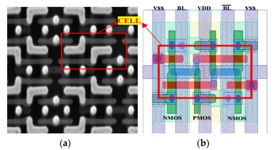
Figure 1.
A photomicrograph (a) and cell layout of HM62V8100i static random-access memory (SRAM) (b).
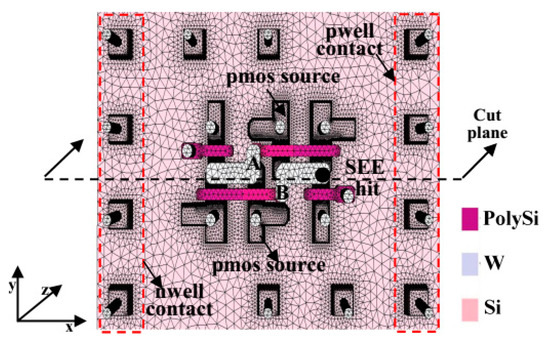
Figure 2.
The top view of the simulated SRAM cell.
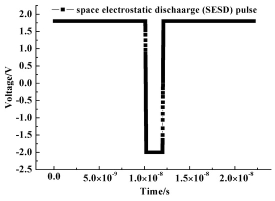
Figure 3.
The characteristics of voltage pulse injected at the power supply node.
Figure 4 reveals the potential evolution for the case of a heavy-ion track generated under the OFF-NMOS drains in the cut–plane direction. The storage node potentials as a function of time are plotted in Figure 5. Before the creation of the ionizing particle, the potentials of node A and node B were 0 V and 1.8 V, indicating that the N-well and P-well potentials were approximately 1.8 V and 0 V, respectively. At this point, the stored bit was set as “0”. Therefore, it was shown that the potentials of the PMOS drain A and PMOS drain B were labeled with blue and green, corresponding to the logical state “0” at t = 0 ps, as depicted in Figure 4. At t = 70 ps, an obvious variation of the potentials of N-well, p-well, and p-substrate are observed for the ion track (respectively, approximately 0.88 V instead of 1.8 V, and 0.03 V instead of −0.77 V). This variation induces a decline in the node B potential and an increase in the node A potential due to the well-known direct charge collection mechanism [19,20] presented in Figure 5. During the diffusion of the electron–hole pairs, at approximately 160 ps, it is shown in Figure 4 that the N-well and P-well near the strike location collapsed. This corresponds to an accumulation of electrons and holes in the N-well and P-well, respectively. As the P-well potential increases and N-well potential drops, the N-source/P-well (P-source/N-well) junction and horizontal P-well/N-well junction were turned on. This results in the quick pull-down of node B potential and pull-up of node A potential, causing the stored bit upset, as depicted in Figure 5. When all of the excess carriers due to the particle were dispersed, the structure returns to the balance and N-well and P-well potentials return to their initial state, respectively, which is shown at approximately 2 ns in Figure 4. At this point, the color of Node A changed from blue to green while the color of Node B switched from green to blue, which indicated that the state of Node A and Node B were locked.
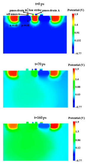
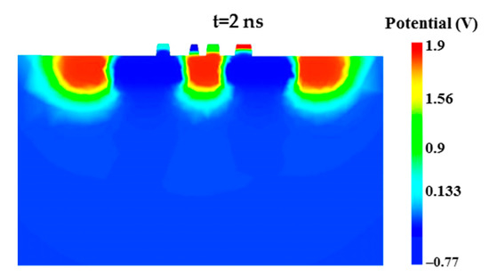
Figure 4.
The potential evolution for the case of SEE in the PMOS source–source (PSS) direction.
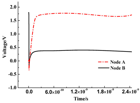
Figure 5.
The storage node potentials as a function of time for SEE.
As compared to the case of SEE radiation, the potential evolution induced by SESD in the PSS direction is shown in Figure 6. The storage node potential evolution versus time is plotted in Figure 7. The potential distributions of the SRAM cell are the same as those induced by SEE before and after the event as a result of the same configuration. During the period of 10 ns < t ≤ 10.2 ns, the injected SESD pulse amplitude drops rapidly from an operating voltage of 1.8 V to a negative peak voltage of −2 V. This large potential change results in the collapse of the N-well and P-well, and as a consequence, their potentials are basically consistent with the substrate potential at t = 10.2 ns, as depicted in Figure 6, indicating that a rail-to-rail potential collapse effect occurs [21]. Subsequently, node A and node B potentials are pulled down to −1 V simultaneously, as shown in Figure 7. The transient rapidly returns from the negative peak voltage to the normal operating value during the period of 12 ns < t ≤ 13 ns, which causes the N-well and P-well potentials to both increase at t = 13 ns, as presented in Figure 6. It is noted in Figure 7 that node A and node B potentials both initially increase from −1 V to 0.7 V, and then the node A potential continues to increase to 1.8 V, while the node B potential drops to 0 V due to the turn-on of the N-source/P-well junction. When the potentials of the unit cell return to equilibrium at t = 14.5 ns, the N-well, P-well and substrate potentials return to their equilibrium state. The final result of this process is the cell upsets.
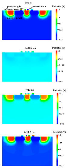
Figure 6.
The potential evolution for the case of SESD in the PSS direction.
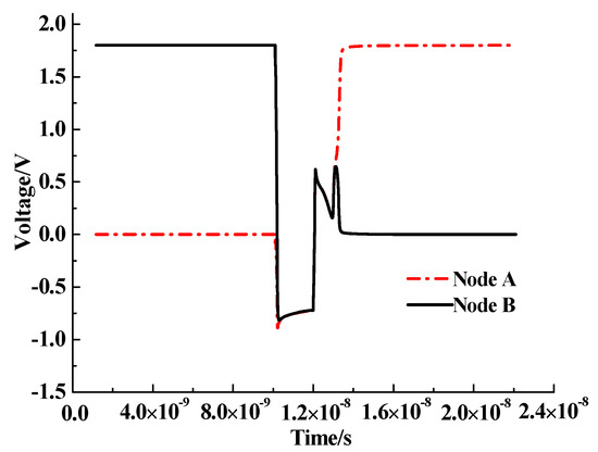
Figure 7.
The storage node potentials as a function of time for SESD.
As mentioned above, it is noted that the root cause of soft error induced by SEE and SESD for SRAM is the variation of the N-well and P-well potentials in the unit cell, causing the pulldown (pullup) of the storage node voltage. The similar upsets for SRAM units are caused by both SEE and SESD radiation. However, there are some differences in the process of the potential evolution of the storage node for SEE and SESD. In the case of SEE, a large number of electron–hole pairs induced by the particle strike are collected by the sensitive reverse-biased PN junction, causing a transient current. This current flow through the struck transistor subsequently induces a voltage transient at the storage node and the time scale of the whole process is tens of picoseconds. In comparison to the mechanism of SEE for SRAM, during the SESD radiation, a rail-to-rail potential collapse between the power supply and the ground was induced by injecting a voltage pulse at the power supply port, thereby causing the variation of the storage node potentials. It is interesting to show that the process of upsets for SESD lasts a few nanoseconds. In addition, we also found that the collapse of potential in N-wells and P-wells caused by SESD is in a much larger scale in terms of time and area. Meanwhile, for modern IC technology, several bits sharing one well (N-well or P-well) is a very common design rule in memory array circuits. This explains why the soft errors by SESD are mostly multi-bit upsets instead of single-bit upsets.
3. Description of the Experimental Setup
In order to further investigate the similarities and differences of soft errors induced by SEE and SESD, the SEE and SESD radiation experiments on the SRAM were performed at the pulsed-laser single event effect facility and SESD test system [15], respectively, at the National Space Science Center. The key parameters of the pulsed laser were as follows: wavelength of 1.064 μm, pulse width 20 ps, spot size 1.7 μm, pulse repetition frequency 1 kHz, and equivalent LET 0.1–120 MeV·cm2/mg [22]. According to the Mitigating Spacecraft Charging Effects Guide (NASA-HDBK-4002A), the ESD generator is recommended as a space discharge simulation source to investigate the SESD effect in the radiation community. The SESD test follows the international standard of ESD testing (IEC 61000-4-2). The measurement setup of the ESD testing with the indirect contact–discharge test mode is shown in Figure 8a, which consists of the horizontal coupling plane (HCP), insulation plane and ESD gun. When the ESD gun excites to the horizontal coupling plane, the device under test (DUT) will be disturbed due to the high ESD-coupled energy. The discharge mode and the discharge voltage of the ESD test system are single discharge and from 500 V to 20 KV, respectively. The test chip is RENESAS HM62V8100i SRAM, fabricated in bulk CMOS 0.18 μm technology. The capacity is 8 Mb, organized as 1 M × 8 b. Plastic package and metal opacity are very difficult issues as they prevent the laser beam from reaching the sensitive areas of SEE. Moreover, the metal layers usually cover a large part of the front-side of an SRAM in deep sub-micron processing. As a consequence, a backside laser test should be adopted after decapping at the silicon layer (the polished chip is shown in Figure 8b). The supply voltage of 3.3 V and the checkerboard pattern are applied during the SEE and SESD testing. Meanwhile, four kinds of test patterns, checkerboard (CB) pattern, complement checkerboard (CBC) pattern, and half-complement checkerboard pattern (all 0 and all 1) were applied in the soft error measurement with SEE and SESD excitation. As a result of omni-directional electromagnetic radiation in SESD tests, the test circuit of SRAM is isolated by the shielded box. The chip function is checked by verifying the storage status of SRAM under different operating conditions of pre-radiation. To reveal more insight into the effect of SEE and SESD on the device, the experimental results were obtained as the average of three rounds of repeated testing for validating their reproducibility.
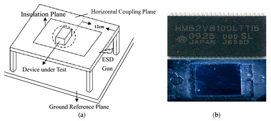
Figure 8.
The schematic diagram of the electrostatic discharge (ESD) test system (a) and the photomicrograph of the polished chip (b).
4. Experimental Results and Discussions
4.1. Comparisons of the Characteristics of Soft Errors
Figure 9 illustrates the characteristics of bit-errors for SRAM as a function of pulsed laser energy compared to SESD voltage in four different test patterns. The number of SRAM errors is displayed in Figure 9a, with the laser energy ranging from 200 pJ to 1.8 nJ. The characteristics of the errors in the memory array induced by SESD (SESD voltage range is from 500 V to 11,000 V) are depicted in Figure 9b.
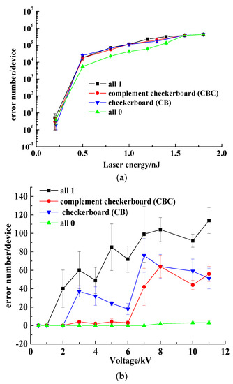
Figure 9.
The characteristics of bit-errors for the SRAM as a function of (a) pulsed laser energy; and (b) SESD voltage.
The number of bit-errors increases significantly with laser energy in four different test patterns, at the same saturated laser energy of 1.8 nJ. It revealed that, under four different test patterns, the laser threshold energy and saturated numbers of errors are similar (about laser threshold energy of 200 pJ and saturated errors of 4 × 10⁵, respectively) in Figure 9a. In contrast, the different test patterns reveal an obvious effect on the number of bit-errors for SESD in Figure 9b. When the SESD voltage increases from 500 V to 11,000 V, the number of bit-errors increases to 114, 51 and 56, respectively, with the all 1 pattern, CBC pattern and CB pattern. However, with all 0 patterns, the number of bit-errors slightly increases to 3 at the SESD voltage of 11,000 V. It is also shown that the SESD threshold voltages are completely different between the four test patterns (2000 V in the all 1 pattern, and 3000 V in the CB and CBC pattern).
Figure 10 illustrates the types of bit-errors for the SRAM with pulsed laser energy and SESD voltage in all 1 patterns. The numbers of multiple-bits upset (MBU) increase significantly after the laser energy of 800 pJ, which is the first occurrence of exceeding the numbers of single-bit upset (SBU), as shown in Figure 10a. All errors are MBU during the SESD radiation, which increase slightly with the SESD radiation ranging from 500 V to 11,000 V, as shown in Figure 10b.
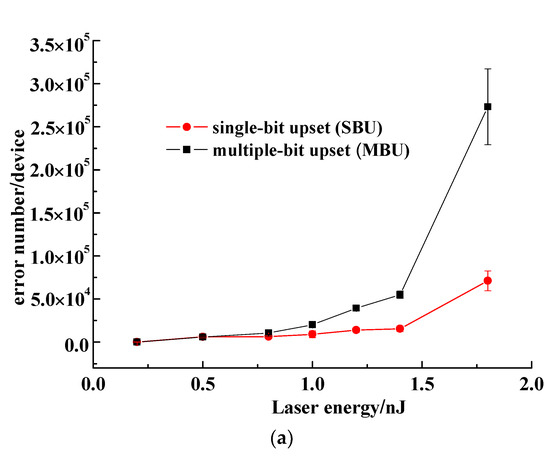
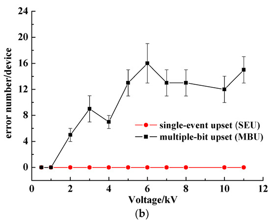
Figure 10.
The types of bit-errors for the SRAM with (a) pulsed laser energy; and (b) SESD voltage.
By comparing the characteristics of bit-errors obtained from the pulsed laser and ESD generator, the similar behaviors of the radiation response have been observed. For example, the numbers of bit-errors will increase with the laser energy and SESD voltage in the all 1 pattern, CB pattern and CBC pattern. The MBU is the major type of bit-error at high laser energy and SESD voltage. However, there are obvious differences between the numbers of bit-errors generated by SEE and SESD in four different test patterns. For pulsed laser excitation, the numbers of bit-errors are not influenced at all by the different test patterns. However, the test patterns show a significant effect on the number of bit-errors for SESD. It was found that all the 1 pattern is the most sensitive to SESD, followed by the CB and CBC pattern, and all 0 patterns lead to the least number of bit-errors. Moreover, the types of bit-errors induced by SEE and SESD also reveal clear differences. Contrary to the SBU and MBU caused by pulsed laser excitation, the SESD test results show that there are only MBU in the memory array.
4.2. Comparisons of the Sensitive Areas of SEE and SESD
In previous work [16], the mapping relationship between the logical address and physical coordinate for HM62V8100i SRAM was established. Figure 11 displays the sensitive areas of the HM62V8100i SRAM to SEE and SESD using pulsed laser and ESD generator excitation for all 1 test pattern. The sensitive areas are marked by a green dot (each dot represents a bit of SRAM) on the front photomicrograph of HM62V8100i SRAM. The laser energy of 1 nJ and SESD voltage of 10,000 V are given for SEE and SESD, respectively.
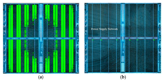
Figure 11.
The sensitive areas of (a) SEE and (b) SESD for the SRAM.
In Figure 11, it is clearly revealed that many bits of the SRAM are very sensitive to SEE and SESD. In addition, Figure 11a shows that the sensitive areas of SEE almost cover the entire memory array of SRAM. Due to probing of each of the SEU-sensitive bits with a pulsed laser, the SEE sensitivity of all bit units can be accessed with the laser energy of 1 nJ. In other words, the SEE sensitivity has a strong relationship with the injected locations of a pulsed laser. In contrast, the sensitive areas of SESD are much smaller and predominantly distributed near the power supply network of SRAM [16], which is identified by the photomicrograph, as shown in Figure 11b. In previous work [17], it was revealed that the transients occurred at the power supply node would lead the output failure in the linear circuit. Furthermore, according to an analysis of the failure mechanism of SESD in Section 2, the possible reason that bit-errors are induced by SESD is linked to the impact of SESD on the power supply circuits of the chip.
4.3. Comparisons of the Effect of Supply Voltage
These types of plots are useful in studying the impact of changing the device supply voltage on the numbers of bit-errors of SRAM. The supply voltages applied vary from 2.8 V to 3.5 V, which is within the voltage range allowed by chip specification, in order to ensure the proper functioning. Figure 12 presents the amounts of bit-errors caused by SEE and SESD as a function of applied supply voltage with the all 1 test pattern. The laser energy of 400 pJ and SESD voltage of 8000 V are applied during the radiation tests, respectively.
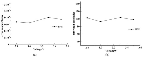
Figure 12.
Error numbers of the SRAM as a function of bias voltages for SEE (a); and SESD (b).
It was distinctly revealed that the amount of bit-errors induced by SEE and SESD for SRAM both change slightly with an increase in the supply voltage from 2.8 V to 3.5 V, as depicted in Figure 12. Meanwhile, the number of bit-errors caused by SEE remains constant (the number of bit-errors is approximately 3500/device) with the increasing supply voltage, as revealed in Figure 12a. Similar behavior is observed in SESD testing. As shown by the experimental results in Figure 12b, the supply voltage has no obvious effect on the number of bit-errors (the number of bit-errors is approximately 100/device). Thus, it is observed that the number of bit-errors induced by SEE and SESD for HM62V8100i SRAM is not voltage-dependently biased in either case. However, the experimental results of the impact of supply voltage on bit units for SRAM show a significant discordance with previous research [23,24]. To elucidate the cause of the discrepancy of bias voltage impact on bit cell, we extracted the detailed circuits of the power supply network for the HM62V8100i SRAM by chip photomicrographs. Figure 13 shows the partial detailed circuit diagram of the power supply network. It is easily deduced that it is a series negative feedback voltage regulator circuit for the power supply circuit of the HM62V8100i SRAM, which mainly includes an external power supply circuit (applying an external voltage to the chip), a regulated power supply circuit, and an internal power supply circuit (applying an internal voltage to memory core). As a result of the wide input and output range of the supply voltage regulator circuit, even if the external supply voltage is low, this circuit can supply enough current to ensure the stable voltage output for the memory core. This is likely the main reason that the number of bit-errors induced by SEE and SESD radiation is not sensitive to supply voltage variations for the HM62V8100I. The SRAMs of plots are useful in studying the impact of changing the device bias voltage on the numbers of bit-errors of SRAM. The supply voltages applied vary from 2.8 V to 3.5 V, which is within the voltage range allowed by chip specification, in order to ensure the proper functioning. Figure 12 presents the amounts of bit-errors caused by SEE and SESD as a function of the applied supply voltage with the all 1 test pattern. The laser energy of 400 pJ and SESD voltage of 8000 V were applied during the radiation tests, respectively.
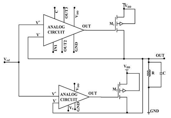
Figure 13.
The partial detail circuits of the power supply network for the HM62V8100i SRAM.
5. Conclusions
The results reported here provide a comprehensive comparison of the soft errors induced by SEE and SESD for the SRAM, aimed at identifying the relevant details of these two effects. The impact mechanisms, the characteristics of the bit-errors, the sensitive areas and the relationship with external stimulus for the SRAM caused by SEE and SESD have been studied. Although the soft errors caused by SEE and SESD in the SRAM circuit were all manifested as bit-upset, it showed that the mechanisms of leading the instantaneous potential change of the sensitive storage node in the memory array are different. Indeed, for the SEE case, the bit-errors are directly induced by the excess charge generated by a particle hit in the memory cells of the SRAM. In contrast, the electromagnetic pulse caused by SESD imposes on the external pins of the SRAM and propagates to the memory circuits. In addition, the potential characteristics of related memory cells are all affected during the propagation. This study demonstrated that the number of soft errors caused by SESD is affected by the test patterns, while the numbers of bit-errors induced by SEE and SESD both increase concomitantly with an increase in pulsed laser energy and SESD voltage. In addition, the experimental results revealed that single-bit-errors and multiple-bit-errors in the SRAM can be obtained by a SEE, while only the multiple-bit-errors could be generated by a SESD. Additionally, the study shows that the sensitive areas of SESD are much smaller and predominantly distributed near the power supply network of the SRAM.
The studies presented here are a first step towards revealing the possible similarities and differences between SEE and SESD. The results from the study can help in the diagnosis of anomalies in spacecraft electronic systems induced by space radiation to further identify the root causes of the anomalies. The methodology presented in this study has shown its effectiveness in differentiating the failures caused by SEE and SESD. The methodology can be directly applied to study other memory devices.
Author Contributions
Conceptualization, R.C., L.C. and J.H.; data curation, Y.L. and Y.M.; formal analysis, X.W. and S.S.; investigation, X.W. and Y.L.; methodology, R.C.; project administration, R.C., L.C. and J.H.; writing—original draft, R.C.; writing—review and editing, R.C. All authors have read and agreed to the published version of the manuscript.
Funding
This work was supported in part by the National Natural Science Foundation of China under Grant 11875060 and11705228, and the Foundation of Key Laboratory of Chinese Academy of Sciences.
Conflicts of Interest
The authors declare no conflict of interest.
References
- Bedingfield, K.; Leach, R.D.; Alexander, M.B. Spacecraft System Failures and Anomalies Attributed to the Natural Space Environment; NASA-RP-1390; NASA Marshall Space Flight Center: Huntsville, AL USA, 1996.
- Koons, H.; Mazur, J.; Selesnick, R.; Blake, J.; Fennell, J. The impact of the space environment on space systems. In Proceedings of the 6th Spacecraft Charging Technology Conference, Hanscom AFB, MA, USA, 2–6 November 1998; pp. 7–11. [Google Scholar]
- Witze, A. Software error doomed Japanese Hitomi spacecraft. Nat. News 2016, 533, 18. [Google Scholar] [CrossRef] [PubMed]
- Ecoffet, R. On-orbit anomalies: Investigation and root cause determination. Presented at the 7th European Space Weather Week, Brugge, Belgium, 15–19 November 2010. [Google Scholar]
- Inguimbert, C.; Bourdarie, S.; Falguere, D.; Paulmier, T.; Ecoffet, R.; Balcon, N. Anomalies of the ADSP 21060 Onboard the DEMETER Satellite. IEEE Trans. Nucl. Sci. 2013, 60, 4067–4073. [Google Scholar] [CrossRef]
- Sedares, L.M.; Redmon, R.J.; Rodriguez, J.; Nowak, B.; Galvan, A. Determining if the Root Cause of an Anomaly is a Single Event Upset. In Proceedings of the SpaceOps 2016 Conference, Daejeon, Korea, 16–20 May 2016; p. 2564. [Google Scholar]
- Binder, D.; Smith, E.C.; Holman, A.B. Satellite Anomalies from Galactic Cosmic Rays. IEEE Trans. Nucl. Sci. 1975, 22, 2675–2680. [Google Scholar] [CrossRef]
- Massengill, L.W.; Diehl-Nagle, S.E.; Wrobel, T.F. Analysis of Transient Radiation Upset in a 2K SRAM. IEEE Trans. Nucl. Sci. 1985, 32, 4026–4030. [Google Scholar] [CrossRef]
- Dodd, P.; Shaneyfelt, A.; Horn, K.; Walsh, D.; Hash, G.; Hill, T.; Draper, B.; Schwank, J.; Sexton, F.; Winokur, P. SEU-sensitive volumes in bulk and SOI SRAMs from first-principles calculations and experiments. IEEE Trans. Nucl. Sci. 2001, 48, 1893–1903. [Google Scholar] [CrossRef]
- Gasiot, G.; Soussan, D.; Glorieux, M.; Bottoni, C.; Roche, P. SER/SEL performances of SRAMs in UTBB FDSOI28 and com-parisons with PDSOI and BULK counterpara ts. In Proceedings of the 2014 IEEE International Reliability Physics Symposium, Waikoloa, HI, USA, 1–5 June 2014; pp. SE.6.1–SE.6.5. [Google Scholar]
- Love, D.; Toomb, D.; Wilkinson, D.; Parkinson, J. Penetrating electron fluctuations associated with GEO spacecraft anomalies. IEEE Trans. Plasma Sci. 2000, 28, 2075–2084. [Google Scholar] [CrossRef]
- Paulmier, T.; Dirassen, B.; Payan, D.; van Eesbeek, M. Material charging in space environment: Experimental test simula-tion and induced conductive mechanisms. IEEE Trans. Dielectr. Electr. Insul. 2009, 16, 682–688. [Google Scholar] [CrossRef]
- Mikaelian, T. Spacecraft charging and hazards to electronics in space. arXiv 2009, arXiv:0906.3884. [Google Scholar]
- Visual TCAD User’s Manual; Cogenda Inc.: Suzhou, China, 2012; Available online: http://www.i-vis.co.jp/pdf/cogenda/Quick_Start_Guide.pdf (accessed on 7 February 2021).
- Chen, R.; Han, J.-W.; Zheng, H.-S.; Yu, Y.-T.; Shangguang, S.-P.; Feng, G.-Q.; Ma, Y.-Q. Comparative research on “high currents” induced by single event latch-up and transient-induced latch-up. Chin. Phys. B 2015, 24, 046103. [Google Scholar] [CrossRef]
- Shen, C.; Ding, G.; Zheng, L. A fully-physical simulation framework for single-event effects in semiconductor devices. Presented at RADECS, Hanscom AFB, MA, USA, 26–29 October 2012. [Google Scholar]
- Chen, R.; Chen, L.; Li, S.; Zhu, X.; Han, J.-W. Comparative Study on the Transients Induced by Single Event Effect and Space Electrostatic Discharge. IEEE Trans. Device Mater. Reliab. 2019, 19, 733–740. [Google Scholar] [CrossRef]
- Ker, M.-D.; Hsu, S.-F. Component-Level Measurement for Transient-Induced Latch-up in CMOS ICs Under System-Level ESD Considerations. IEEE Trans. Device Mater. Reliab. 2006, 6, 461–472. [Google Scholar] [CrossRef]
- Dodd, P. Physics-based simulation of single-event effects. IEEE Trans. Device Mater. Reliab. 2005, 5, 343–357. [Google Scholar] [CrossRef]
- Dodd, P.; Massengill, L. Basic mechanisms and modeling of single-event upset in digital microelectronics. IEEE Trans. Nucl. Sci. 2003, 50, 583–602. [Google Scholar] [CrossRef]
- Mavis, D.G.; Alexander, D.R.; Dinger, G.L. A Chip-Level modeling approach for rail span collapse and survivability analysis. IEEE Trans. Nucl. Sci. 1989, 36, 2239–2246. [Google Scholar] [CrossRef]
- Yu, Y.-T.; Han, J.-W.; Feng, G.-Q.; Cai, M.-H.; Chen, R. Correction of Single Event Latchup Rate Prediction Using Pulsed Laser Mapping Test. IEEE Trans. Nucl. Sci. 2015, 62, 565–570. [Google Scholar] [CrossRef]
- Barak, J.; Levinson, J.; Akkerman, A.; Adler, E.; Zentner, A.; David, D.; Lifshitz, Y.; Hass, M.; Fischer, B.E.; Schlogl, M.; et al. Scaling of SEU mapping and cross section, and proton induced SEU at reduced sup-ply voltage. IEEE Trans. Nucl. Sci. 1999, 46, 1342–1353. [Google Scholar] [CrossRef]
- Petrov, A.G.; Nikiforov, A.Y.; Boruzdina, A.B.; Ulanova, A.V.; Yanenko, A.V. Memory chips and units radiation tolerance dependence on supply volt-age during irradiation and test. Facta Univ. Ser. Electron. Energetics 2018, 31, 131–140. [Google Scholar] [CrossRef]


Publisher’s Note: MDPI stays neutral with regard to jurisdictional claims in published maps and institutional affiliations. |
© 2021 by the authors. Licensee MDPI, Basel, Switzerland. This article is an open access article distributed under the terms and conditions of the Creative Commons Attribution (CC BY) license (http://creativecommons.org/licenses/by/4.0/).