
The Study of the Single Event Effect in AlGaN/GaN HEMT Based on a Cascode Structure


Abstract
1. Introduction
2. Simulation Results and Discussion
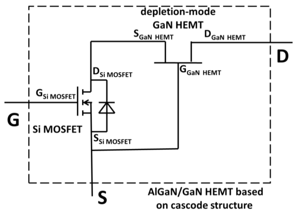
2.1. Modeling
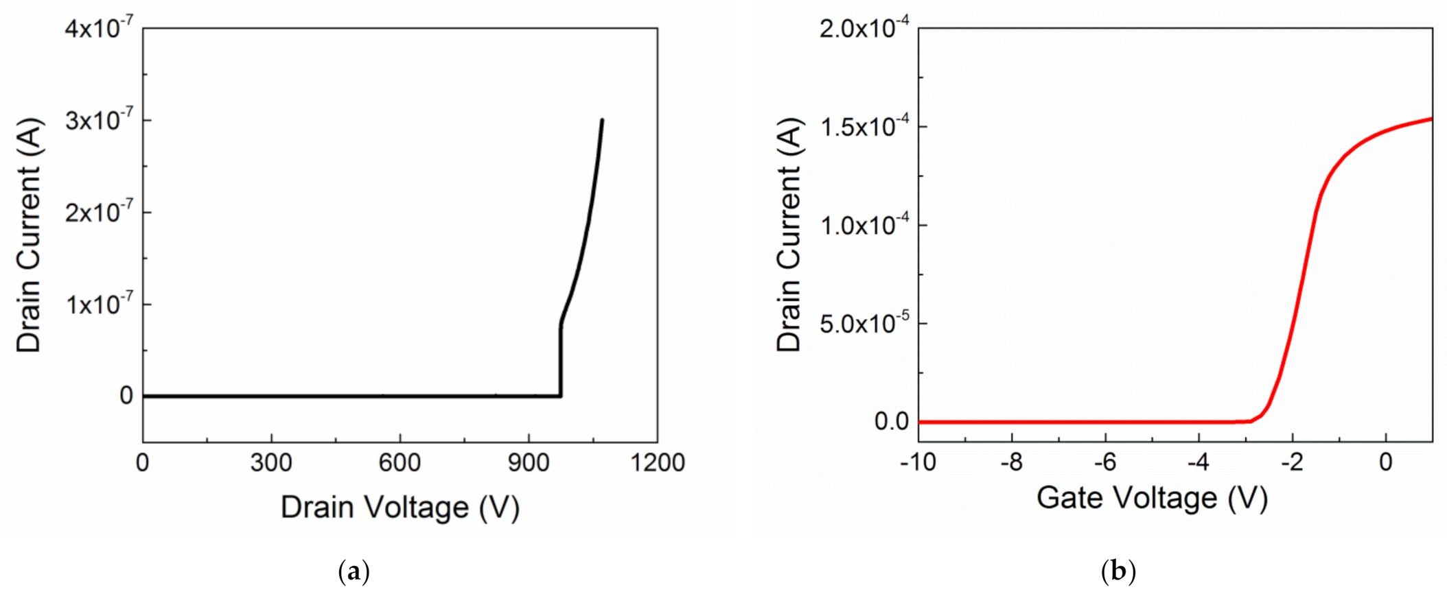
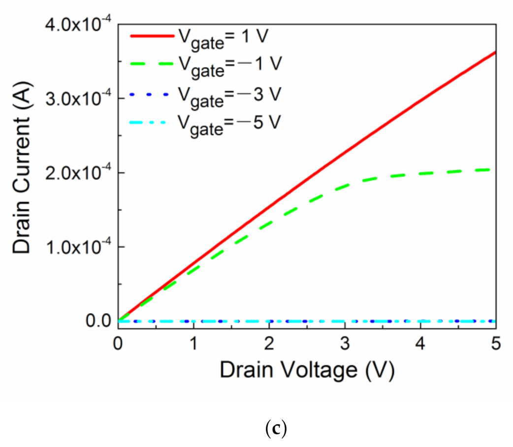
2.2. Simulation Results and Discussion
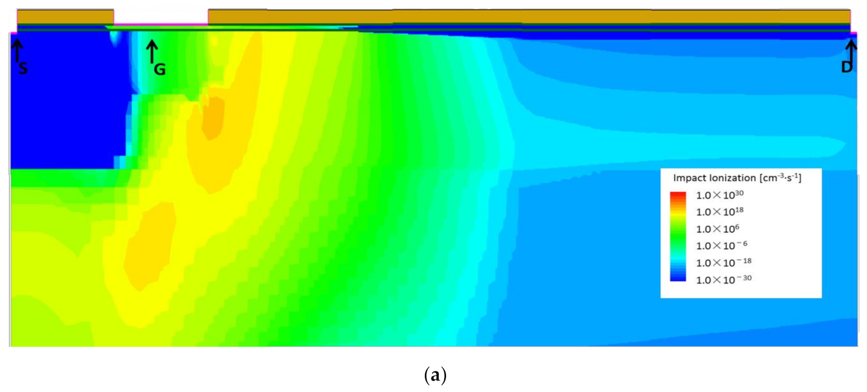
2.2.1. SEB Characteristics of HMET
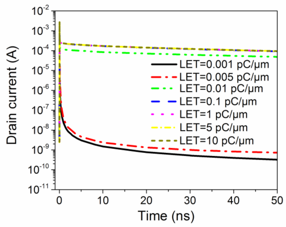
2.2.2. Influence Factors of SEB
- Heavy-ion energy
- Heavy-ion track length
- Sensitive region of SEB
2.2.3. The Failure Mechanism of SEB
3. Heavy-Ion Experimental Results and Discussion
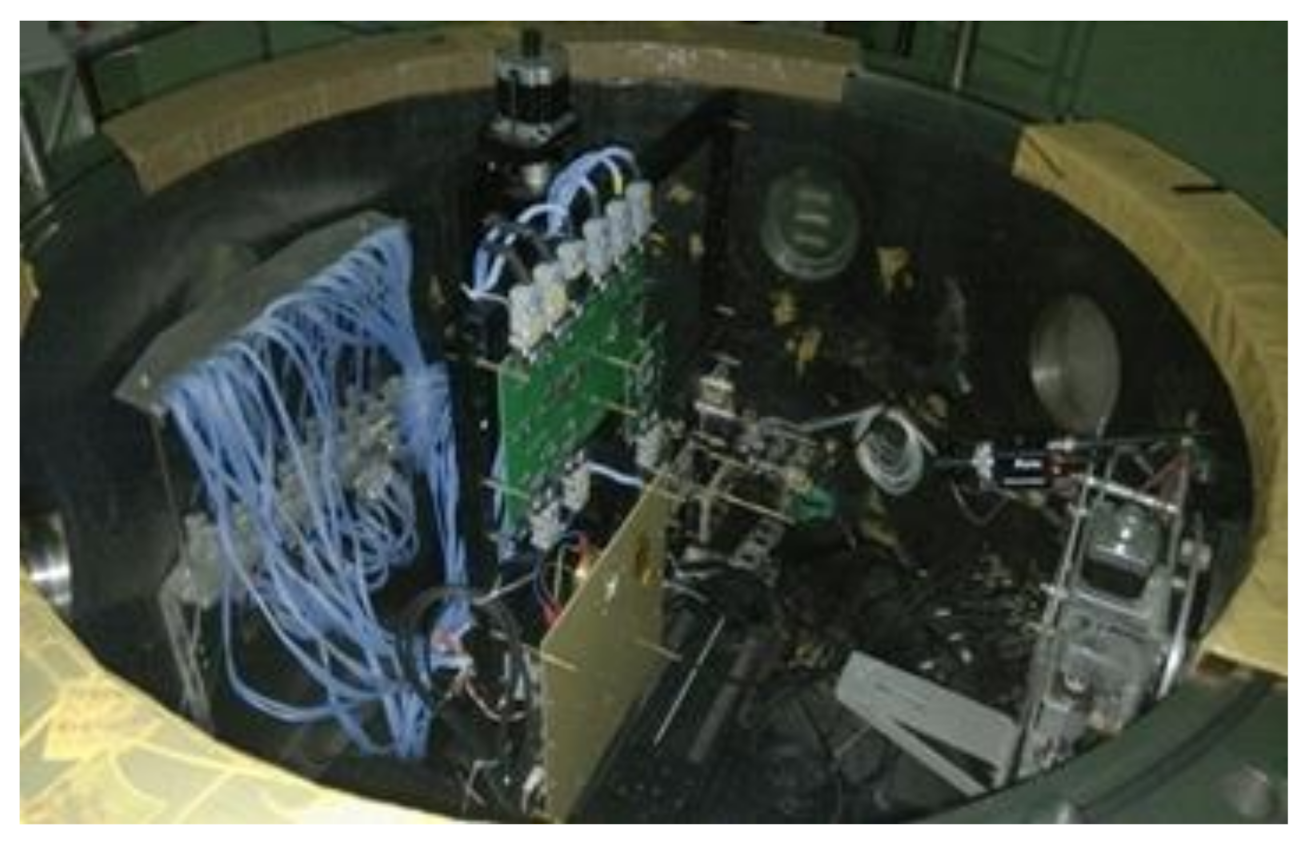
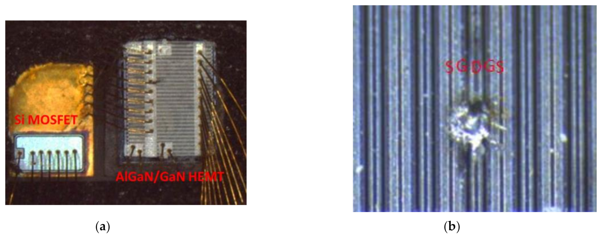
3.1. Experiment Samples and Setup
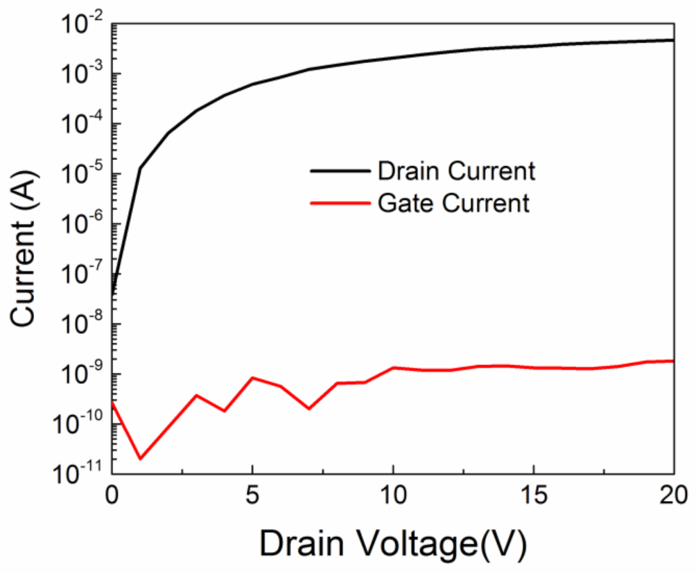
3.2. Experiment results and discussion
4. Conclusions
Author Contributions
Funding
Conflicts of Interest
References
- Efthymiou, L.; Longobardi, G.; Camuso, G.; Chien, T.; Chen, M.; Udrea, F. On the physical operation and optimization of the p-GaN gate in normally-off GaN HEMT devices. Appl. Phys. Lett. 2017, 110, 123502. [Google Scholar] [CrossRef]
- Hwang, I.; Choi, H.; Lee, J.; Choi, H.; Kim, J.; Ha, J.; Um, C.-H.; Hwang, S.-K.; Oh, J.; Kim, J.-Y.; et al. 1.6 kV, 2.9 mΩ cm2 normally-off p-GaN HEMT device. In Proceedings of the International Symposium on Power Semiconductor Devices and ICs, Bruges, Belgium, 3–7 June 2012; pp. 41–44. [Google Scholar]
- Sun, W.-W.; Zheng, X.-F.; Fan, S.; Wang, C.; Du, M.; Zhang, K.; Chen, W.-W.; Cao, Y.-R.; Mao, W.; Ma, X.-H. Degradation mechanism of enhancement-mode AlGaN/GaN HEMTs using fluorine ion implantation under the on-state gate overdrive stress. Chin. Phys. B 2015, 24, 017303. [Google Scholar] [CrossRef]
- Chen, H.; Wang, M.; Chen, K.J. Self-aligned enhancement-mode AlGaN/GaN HEMTs using 25 keV fluorine ion implantation. In Proceedings of the 68th Device Research Conference, South Bend, IN, USA, 21–23 June 2010. [Google Scholar]
- Yatabe, Z.; Hori, Y.; Ma, W.-C.; Asubar, J.T.; Akazawa, M.; Sato, T.; Hashizume, T. Characterization of electronic states at insulator/(Al)GaN interfaces for improved insulated gate and surface passivation structures of GaN-based transistors. Jpn. J. Appl. Phys. 2014, 53, 100213. [Google Scholar] [CrossRef]
- Zhao, Q.-T. Fabrication and Characterization of Enhancement-Mode High-κ LaLuO3-AlGaN/GaN MIS-HEMTs. IEEE Trans. Electron Devices 2013, 60, 3040–3046. [Google Scholar]
- Saito, W.; Saito, Y.; Fujimoto, H.; Yoshioka, A.; Ohno, T.; Naka, T.; Sugiyama, T. Switching controllability of high voltage GaN-HEMTs and the cascode connection. In Proceedings of the 24th International Symposium on Power Semiconductor Devices and ICs, Bruges, Belgium, 3–7 June 2012; pp. 229–232. [Google Scholar]
- Liu, Z.; Huang, X.; Lee, F.C.; Li, Q. Simulation model development and verification for high voltage GaN HEMT in cascode structure. In Proceedings of the 2013 IEEE Energy Conversion Congress and Exposition, Denver, CO, USA, 15–19 September 2013. [Google Scholar]
- Sun, X.; Saadat, O.I.; Chen, J.; Zhang, E.X.; Cui, S.; Palacios, T.; Fleetwood, D.M.; Ma, T.P. Total-Ionizing-Dose Radiation Effects in AlGaN/GaN HEMTs and MOS-HEMTs. IEEE Trans. Nucl. Sci. 2013, 60, 4074–4079. [Google Scholar] [CrossRef]
- Jiang, R.; Zhang, E.X.; McCurdy, M.W.; Wang, P.; Gong, H.; Yan, D.; Schrimpf, R.D.; Fleetwood, D.M. Dose-Rate Dependence of the Total-Ionizing-Dose Response of GaN-Based HEMTs. IEEE Trans. Nucl. Sci. 2019, 66, 170–176. [Google Scholar] [CrossRef]
- Aktas, O.; Kuliev, A.; Kumar, V.; Schwindt, R.; Toshkov, S.; Costescu, D.; Stubbins, J.; Adesida, I. 60Co gamma radiation effects on DC, RF, and pulsed I–V characteristics of AlGaN/GaN HEMTs. Solid State Electron. 2004, 48, 471–475. [Google Scholar] [CrossRef]
- Stocco, A.; Gerardin, S.; Bisi, D.; Dalcanale, S.; Rampazzo, F.; Meneghini, M.; Meneghesso, G.; Grünenpütt, J.; Lambert, B.; Blanck, H.; et al. Proton induced trapping effect on space compatible GaN HEMTs. Microelectron. Reliab. 2014, 54, 2213–2216. [Google Scholar] [CrossRef]
- Kim, B.-J.; Ahn, S.; Ren, F.; Pearton, S.; Yang, G. Effects of proton irradiation and thermal annealing on off-state step-stressed AlGaN/GaN high electron mobility transistors. J. Vac. Sci. Technol. B 2016, 34, 041231. [Google Scholar] [CrossRef]
- Ives, N.E.; Chen, J.; Witulski, A.F.; Schrimpf, R.D.; Fleetwood, D.M.; Bruce, R.W.; McCurdy, M.W.; Zhang, E.X.; Massengill, L.W. Effects of Proton-Induced Displacement Damage on Gallium Nitride HEMTs in RF Power Amplifier Applications. IEEE Trans. Nucl. Sci. 2015, 62, 2417–2422. [Google Scholar] [CrossRef]
- Koehler, A.D.; Anderson, T.J.; Khachatrian, A.; Roche, N.J.-H.; Buchner, S.; Weaver, B.D.; Hobart, K.D.; Kub, F.J. (Invited) Displacement Damage and Single Event Effects in AlGaN/GaN HEMTs. ECS Trans. 2017, 75, 13–20. [Google Scholar] [CrossRef]
- Zerarka, M.; Austin, P.; Bensoussan, A.; Morancho, F.; Durier, A. TCAD Simulation of the Single Event Effects in Normally-OFF GaN Transistors After Heavy Ion Radiation. IEEE Trans. Nucl. Sci. 2017, 64, 2242–2249. [Google Scholar] [CrossRef]
- Zerarka, M.; Crepel, O. Radiation robustness of normally-off GaN/HEMT power transistors (COTS). Microelectron. Reliab. 2018, 90, 984–991. [Google Scholar] [CrossRef]
- Salame, C.-T.; Hoffmann, A.; Mialhe, P.; Charles, J.P.; Kerns, D.V.; Kerns, S.E. Size effect on seb cross-section of VDMOSFETs. Radiat. Eff. Defects Solids 2000, 152, 191–200. [Google Scholar] [CrossRef]
- Tang, Z.; Li, X.; Tan, K.; Liu, C.; Chen, X.; Fu, X. The Progress of SEB and SEGR Irradiation Hardening Technology for Power MOSFET. In Proceedings of the International Conference on Radiation Effects of Electronic Devices (ICREED), Beijing, China, 16–18 May 2018; pp. 1–4. [Google Scholar]
- Li, Z.C.; Li, S.Y.; Liu, J.C.; Cao, Z.; Yang, S.Y. Measurements of the Cross Sections of the Single Event Burnout (SEB) for the Power MOSFET. At. Energy Sci. Technol. 2004, 38, 395–398. [Google Scholar]
- Bulutay, C. Electron initiated impact ionization in AlGaN alloys. Semicond. Sci. Technol. 2002, 17, L59. [Google Scholar] [CrossRef]
- Rowena, I.B.; Selvaraj, S.L.; Egawa, T. Buffer Thickness Contribution to Suppress Vertical Leakage Current With High Breakdown Field (2.3 MV/cm) for GaN on Si. IEEE Electron Device Lett. 2011, 32, 1534–1536. [Google Scholar] [CrossRef]
- Visalli, D.; Van Hove, M.; Srivastava, P.; Derluyn, J.; Das, J.; Leys, M.; DeGroote, S.; Cheng, K.; Germain, M.; Borghs, G. Experimental and simulation study of breakdown voltage enhancement of AlGaN/GaN heterostructures by Si substrate removal. Appl. Phys. Lett. 2010, 97, 113501. [Google Scholar] [CrossRef]
- Onoda, S.; Hasuike, A.; Nabeshima, Y.; Sasaki, H.; Yajima, K.; Sato, S.-I.; Ohshima, T. Enhanced Charge Collection by Single Ion Strike in AlGaN/GaN HEMTs. IEEE Trans. Nucl. Sci. 2013, 60, 4446–4450. [Google Scholar] [CrossRef]


| Heavy-Ion | Energy (MeV) | LET(GaN) (MeV·cm2/mg) | Strike in GaN (μm) |
|---|---|---|---|
| 74Ge11,20+ | 210 | 28.5 | 16.21 |
Publisher’s Note: MDPI stays neutral with regard to jurisdictional claims in published maps and institutional affiliations. |
© 2021 by the authors. Licensee MDPI, Basel, Switzerland. This article is an open access article distributed under the terms and conditions of the Creative Commons Attribution (CC BY) license (http://creativecommons.org/licenses/by/4.0/).
Share and Cite
Liang, Y.; Chen, R.; Han, J.; Wang, X.; Chen, Q.; Yang, H. The Study of the Single Event Effect in AlGaN/GaN HEMT Based on a Cascode Structure. Electronics 2021, 10, 440. https://doi.org/10.3390/electronics10040440
Liang Y, Chen R, Han J, Wang X, Chen Q, Yang H. The Study of the Single Event Effect in AlGaN/GaN HEMT Based on a Cascode Structure. Electronics. 2021; 10(4):440. https://doi.org/10.3390/electronics10040440
Chicago/Turabian StyleLiang, Yanan, Rui Chen, Jianwei Han, Xuan Wang, Qian Chen, and Han Yang. 2021. "The Study of the Single Event Effect in AlGaN/GaN HEMT Based on a Cascode Structure" Electronics 10, no. 4: 440. https://doi.org/10.3390/electronics10040440
APA StyleLiang, Y., Chen, R., Han, J., Wang, X., Chen, Q., & Yang, H. (2021). The Study of the Single Event Effect in AlGaN/GaN HEMT Based on a Cascode Structure. Electronics, 10(4), 440. https://doi.org/10.3390/electronics10040440