Article

Breakdown Behavior of GaAs PCSS with a Backside-Light-Triggered Coplanar Electrode Structure

1
College of Advanced Interdisciplinary Studies, National University of Defense Technology, Changsha 410073, China
2
State Key Laboratory of Pulsed Power Laser Technology, College of Advanced Interdisciplinary Studies, National University of Defense Technology, Changsha 410073, China
*
Authors to whom correspondence should be addressed.
Electronics 2021, 10(3), 357; https://doi.org/10.3390/electronics10030357
Submission received: 29 December 2020 / Revised: 17 January 2021 / Accepted: 29 January 2021 / Published: 2 February 2021
(This article belongs to the Section Semiconductor Devices)

Abstract

:
The competitive relationship between the surface flashover of the coplanar electrodes and the body current channel was investigated. Breakdown behavior of GaAs photo-conductive semiconductor switch (PCSS) with a backside-light-receiving coplanar electrode structure was studied in this paper. GaAs PCSS was triggered by the laser pulse with an extrinsic absorption wavelength of 1064 nm. Special insulating construction was designed for GaAs PCSS, while the surface of the electrodes was encapsulated with transparent insulating adhesive. Our first set of experiments was at a bias voltage of 8 kV, and the surface flashover breakdown of GaAs PCSS was observed with 10 Hz triggering laser pulse. In the second experiment, at a bias voltage of 6 kV, the body current channel breakdown appeared on the backside of the GaAs PCSS. Compared with these results, the existence of a competitive relationship between the surface flashover breakdown and the body current channel breakdown of the GaAs PCSS was confirmed. When the bias voltage is set within a certain range (just reaching avalanche mode), GaAs PCSS with a backside-light-receiving coplanar electrode structure will undergo the body current channel breakdown. This finding is also consistent with the simulation results.

1. Introduction

Photoconductive semiconductor switches (PCSSs) have been gradually used in ultrafast electronics and high-power pulse technology because of their essential characteristics: fast response, low jitter, optical trigger isolation, MHz working repetition rates, and compact structure [1,2,3,4,5,6,7,8]. GaAs PCSS is a direct-gap semiconductor with a bandgap of 1.42 eV, which corresponds to intrinsic absorbance at 876 nm. It has extrinsic absorption at higher wavelengths. The lifetime of extrinsic carriers of GaAs PCSS spans from picoseconds to nanoseconds, which makes GaAs PCSS suitable for the generation of a narrow pulse if such short conducting times are required. Two working modes of the GaAs PCSS are linear and nonlinear mode [9,10,11,12]. Under the linear mode, the generation of a photon is accompanied by the generation of an electron-hole pair. All carriers that pass through the switch are generated by incident electrons. Excluding the effects of an external electric circuit, the conducting time of the PCSS depends on the pulse rise time. A high-energy laser pulse is required to trigger the conducting stage of the PCSS under the linear mode, which limits its application in the generation of ultra-wide spectrum pulses at a high repetition frequency. Nonlinear mode is also called avalanche mode or high-gain mode. It appears when GaAs PCSS with a high-bias electric field is triggered by a light pulse, and the incident photons generate several electron-hole pairs. These carriers collide and ionize to generate enough electron-hole pairs to render the PCSS conductive. The energy of the laser pulse required to trigger the conduction stage of the PCSS under the avalanche mode is three to five orders of magnitude lower than in the case of the linear working mode. Therefore, under the avalanche mode, compact laser diodes can be employed as a triggering light source to replace high-energy laser.
On the basis of the relative position of the electrodes, photoconductive devices can have a coplanar electrode structure and a vertical geometry electrode structure. In the coplanar electrode structure, positive and negative electrodes of the PCSS are normally placed on the same side of the semiconductor material. This electrode configuration provides easy manufacturing, simple semiconductor processing, large laser incident surface between the electrodes, and straightforward adjustment of the space between the electrodes to meet different requirements [13,14,15,16,17,18,19]. However, the surface breakdown of the coplanar electrode structure is more likely to occur under high voltage. The electric field required for the surface breakdown is more than one order of magnitude lower than that for the breakdown of a dielectric body. Therefore, the electrode surface of the PCSS with coplanar electrode structure should be modified to increase the operating voltage of the device. In previous studies, the flashover voltage of the back-triggered PCSS was found to be higher than that of the front-triggered one. It is generally considered that the illuminated area and the electrodes side are separated at the two sides of the PCSS when back-triggered.
In this paper, GaAs PCSS with backside-light-receiving coplanar electrode structure is established. Through semiconductor simulation, a typical phenomenon of body current channel breakdown was found in certain bias voltage condition, instead of common surface flashover. When GaAs PCSS was back-triggered, a competitive relationship between surface flashover breakdown and the body current channel breakdown can be observed. Experiments were designed to prove this competitive relationship. The breakdown caused by the surface flashover of the coplanar electrodes may be inhibited to a certain extent if the avalanche current filament path generated in the PCSS device is at a reasonable distance from the surface of the coplanar electrodes, and whether the surface where the coplanar electrodes are embedded is insulated to modulate the spatial distribution of the surface current. It can be supplied to produce further improvements in the performance of GaAs PCSS.

2. Experimental Setup and Typical Waveform

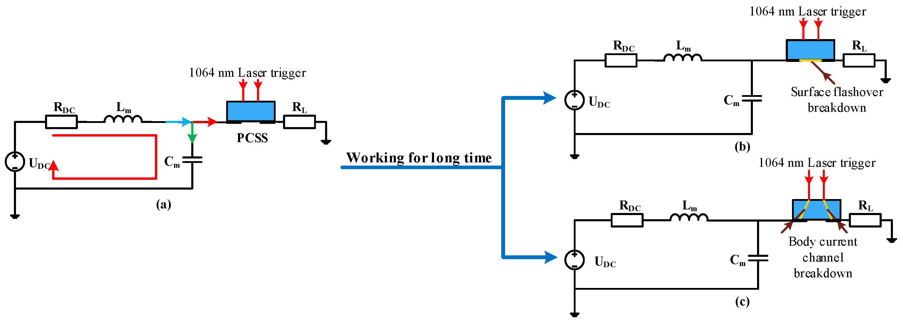
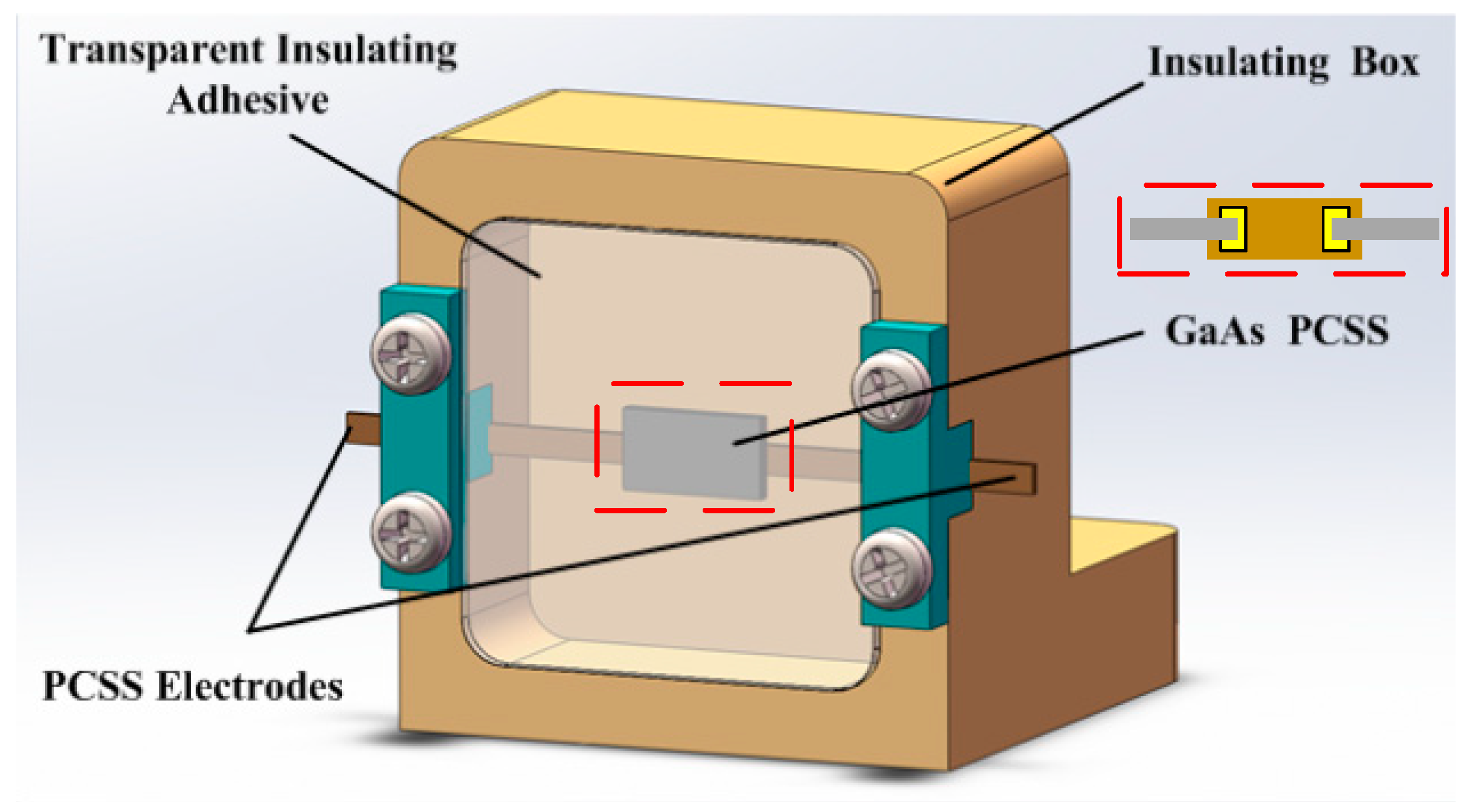
2.1. Experimental Circuit and PCSS Structure

The experimental circuit of the GaAs PCSS featuring the backside-light-triggered coplanar electrodes is shown in Figure 1a. RDC, 5 kΩ water resistance, was used as current-limiting resistance, with the equivalent inductance of 10 µH. A ceramic capacitor Cm with a capacitance value of 20 nF was used as a charging capacitor. Composed of three 100 Ω non-inductive resistances in parallel connection, RL were used as load resistance to reduce stray inductance Lm. The equivalent resistance value of the load resistance RL was 33.3 Ω. The load output waveform, VR, was measured using a high-impedance voltage probe. GaAs PCSS was triggered in the extrinsic absorption mode. The experiment was carried out using a high-power pulsed laser with an extrinsic absorption wavelength of 1064 nm. The width of the laser pulse was 1.6 ns and laser pulse energy was about 60 mJ. To protect the PCSS device, we used a 1:100 attenuation lens to weaken the laser energy. The actual incident laser pulse energy of ≈0.6 mJ was determined. To make the position of the laser pulse incident point easily adjustable, we mounted the base of the experimental platform on the optical guiding rail. The incident laser can be ensured to shine on the backside of the electrode of the photoconductive device by adjusting the experimental platform to a proper location along the guiding rail. As the whole experimental platform was operating under the air conditions, we placed insulation paper at the contact points of the platform device to ensure complete high-voltage insulation of the platform. A photoelectric probe was placed in the vicinity of the GaAs PCSS to detect the waveform of the triggering light pulse VL.
The structure of GaAs PCSS used in this experiment is shown in Figure 2. It had a dark electrical resistivity of ≈5 × 10⁷ Ω/cm and electron mobility of about 8500 cm2/V·s. With the dimensions of 14 × 6 × 0.6 mm, it was equipped with coplanar electrodes. Moreover, its electrode gap between the electrodes was 5 mm. The electrode was made of Au/Ge/Ni alloy, and good ohmic contact was formed on the surface of the GaAs by subsequently applied evaporation, deposition, and high-temperature annealing steps. To avoid thermal damage of the photoconductive device during the welding process, we used the Sn42Bi58 low-temperature welding paste to weld the photoconductive device by hot-air welding. Copper planar wires with a length of 1 mm were stretched out from each end of the electrode. Since the GaAs device used in the experiment was equipped with coplanar electrodes, the dielectric voltage-withstand performance of the device should be improved. A kind of silicone gel adhesive (Sylgard 184) was used to ensure electric insulation on the surfaces of electrodes. As shown in Figure 2, Sylgard 184 was poured into a pre-designed packing box in which the photoconductive device was placed. The whole packing box was then subjected to a degassing process. Finally, the packing box was placed in the vacuum oven and cured by constant heating. The cured packaging box was taken out after cooling down in the ambient environment.

2.2. Waveforms of GaAs PCSS Working in Avalanche Mode

The waveform of output current for different bias voltages Figure 3a shows that at a low bias voltage (2 kV), GaAs PCSS worked in linear mode. When the voltage was gradually increased, PCSS gradually shifted from the linear mode to the avalanche mode. At a bias voltage of 6 kV, the stable avalanche mode of the GaAs PCSS was achieved. In the first set of experiments, the triggering of the GaAs PCSS at 10 Hz repetition frequency was performed at a stable bias voltage of 8 kV. Then, in a second experiment, the same GaAs PCSS was used at 6 kV for long-time working.
Figure 4 shows working behavior of the PCSS gradually decreased for long period of time until the device broke down. Its working state is divided by three stages. At first, GaAs PCSS works in avalanche mode normally. Working for a long period of time, GaAs PCSS begins to occur damage on its surface. This is referred to as the pre-breakdown state. Output current also goes down a little. Finally, as the damage accumulates, it is totally broken down and its output current no longer declines.
The lifetime of the GaAs avalanche semiconductor switch by back-side triggering (relative to electrode position) was investigated experimentally. The tests were given to three groups. One switch biased at 6 kV and another one biased at 8 kV were tested in a group. Once the pre-breakdown state was observed in the tests, the switch was defined as damage. The number of pulses already operated was defined as the lifetime of the switch, and the average lifetime for each test is presented in Table 1.
The longevity achieved with body current channel breakdown at bias voltage of 6 kV was 3–5 times longer than that with surface flashover at 8 kV. In addition, the GaAs avalanche semiconductor switch only operated 4 × 10⁵ pulses with surface flashover breakdown at 10 Hz in our experiment. A longer lifetime up to 106 shots was achieved with body current channel breakdown when the device operated at 10 Hz. It was obvious that the body current channel breakdown mode was with lower bias voltage and higher quality to withstand voltage than surface flashover breakdown. This can be used to explain results of lifetime tests.

2.3. Microscopic Observation for Breakdown GaAs PCSS

As shown in Figure 5, the damaged PCSS was taken out from silicone gel adhesive and further observed by scanning electron microscopy (SEM). The surface flashover breakdown appeared on the surface of the side with embedded coplanar electrodes, while ablated marks appeared on the anode. A white, curved mark in Figure 5a shows the exact location of surface flashover under the bias voltage of 8 kV. The breakdown area between the electrodes, highlighted in the red frame, was investigated. It can be seen that the surface flashover channel went through the two electrodes without any changes on the backside of the device. In Figure 5b, breakdown points are shown on the backside of GaAs PCSS for the 6 kV experiment. This indicates prominent breakdown point(s) with dielectric sputtering, and traces of surface filament current discharge can be also observed. This means body current channel breakdown was formed through two sides of the PCSS.
The experimental results show the effect of the bias voltage on the breakdown mechanism of the GaAs PCSS device. Higher bias voltage (8 kV) in the first experiment induced damage due to the surface flashover breakdown. On the other side, a lower bias voltage (6 kV) in the second experiment induced the damage due to the body current channel breakdown.

3. Discussion and Analysis of Breakdown Behavior for Different Bias Voltage

3.1. Analysis of the Avalanche Process and Discharge Paths

When the bias voltage of the GaAs PCSS is higher than the avalanche threshold voltage, space charges are generated inside the semiconductor material triggered by the light pulse. The space charge density inside the semiconductor, ρ, can be obtained according to the Poisson equation and the charge continuity equation in Equation (1).
{ E = ρ ε ε 0 j = n 0 e v d ( E ) d ρ d t = j
For GaAs semiconductor material, n0 is equilibrium carrier concentration. νd is flowing speed of carrier, which is related to electric field E in the direction of carrier flow. Three formulas in Equation (1) can be further developed as follows:
d ρ d t = [ n 0 e v d ( E ) ] = n 0 e d v d d E E = n 0 e ε ε 0 d v d d E ρ = ρ τ d
τd is defined as the dielectric relaxation time, which represents time constant for space charge attenuation. Space charge density ρ can be obtained as exponential form.
ρ = ρ 0 exp ( t τ d )
When the electric field is at a relatively high level (3.2–4.2 kV/cm), the drift velocity of electrons in GaAs decreases, and there is a negative differential mobility region. This has been named as the Gunn effect. Under Gunn conditions, τd becomes negative, indicating that the space charge does not disappear but increases with time. Once a small electric dipole layer forms in the semiconductor, it will continuously grow during the movement of charge carriers, forming a high-field charge domain. Obviously, when the transit time is much longer than the dielectric relaxation time τd, the charge domains can fully grow and maintain at a stable level, as shown in Equation (4).
L v d > > τ d = ε ε 0 n 0 e ( d v d d E ) 1
L is drift path length of the carrier. Ideal Gunn effect can be obtained by the conversion of Equation (4) with path integral form:
0 L n d L > > ε ε 0 v d e ( d v d d E ) 1 1 × 10 12 cm 2
Thus, it can be concluded that when the conditions specified by Equation (5) are met, the stable charge domains will be generated in GaAs PCSS. This means the trend of stable charge channel is not always along shortest path and is also dependent on photon-generated carrier concentration. It can be used to explain competitive relationship between two breakdown modes. Although breakdown path of body current channel is longer than surface flashover, there is higher carrier concentration on backside of GaAs PCSS with backside-light triggered. Thus, it is possible for two different kinds of breakdown modes to occur.
Generally, a dipole composed of an excess electron and an electron-depleted hole will be generated at the light-triggering position. The dipole creates an electric field at this position, and the internal electric field strength is stronger than the bias voltage. This electric field will force the electron in the dipole to move at a speed lower than that of the external electrons. As a result, since the trailing electrons behind the dipole arrive relatively fast, the excess electrons accumulate in the region. Similarly, as the electrons in front of the dipole also leave relatively fast, the electron-depleted holes in the depletion region also accumulate. The electric field in this area gradually increases, while the external electric field gradually decreases. When these two electric fields reach equilibrium, the dipole does not grow further, forming a charge domain. This charge domain drifts from the cathode to the anode under the influence of the electric field.

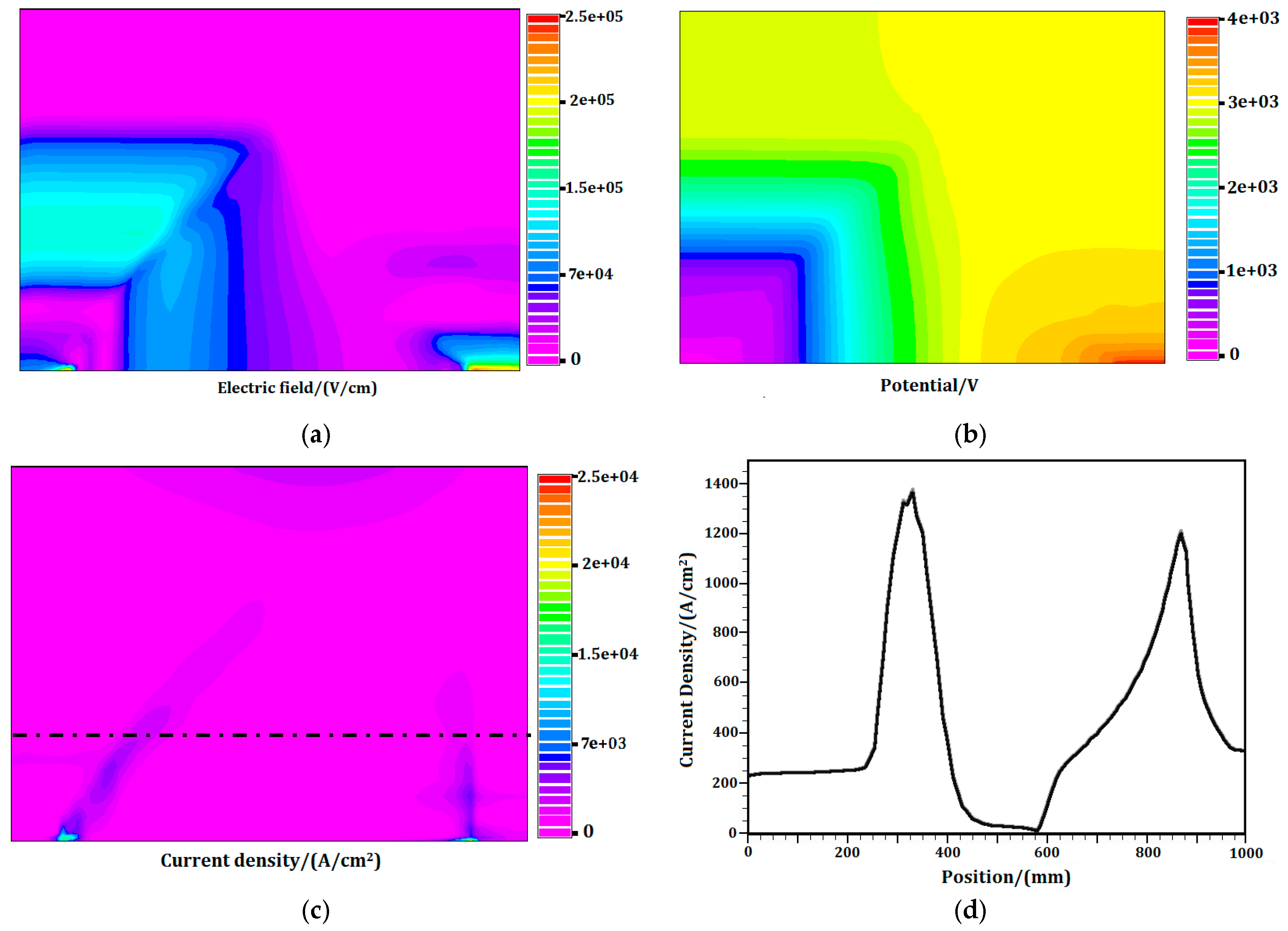
3.2. Simulation Analysis for Avalanche GaAs PCSS

To simulate the breakdown behavior of the GaAs PCSS with a backside-light-receiving coplanar electrode structure, we used the Silvaco TCAD semiconductor simulation software. In the two-dimensional simulation, the lower edge is the contact electrode of the GaAs PCSS, and the remaining part is the substrate of the GaAs photoconductive material. It assumes that GaAs semiconductor is n-type and its doping concentration is 107 cm-3. Voltage on cathode was set as 6 kV. Carrier–carrier scattering mobility model (ccsmob), parallel electric field-dependent mobility model (fldmob), Selberherr’s impact ionization model (impact selb), and Shockley–Read–Hall recombination model (srh) were used to describe carrier behavior in the semiconductor simulation. Simulation for transient characteristics was taken from 0 ns to 10 ns, which was with a time step of 0.01 ns. The current density and concentration of photogenerated carriers in the device were simulated separately. The simulation results, shown in Figure 6, confirm that there was a bulk current channel inside the GaAs PCSS device.
These results show that in a certain range of bias voltage, GaAs PCSS with a backside-light-receiving coplanar electrode structure will undergo body current channel breakdown, being consistent with the simulation results. Meanwhile, the comparison of results shows that there is a competitive relationship between the surface flashover breakdown and the body current channel breakdown within the coplanar electrodes. In the first experiment, although the surface of the device was completely insulated, the surface breakdown flashover still occurred when the GaAs PCSS worked at a relatively high bias voltage. This phenomenon was partly related to the fact that the experimental platform was powered by a continuous DC power supply. The existence of a large steady bias voltage between the two electrodes of GaAs PCSS device likely yielded the surface breakdown flashover before the body current channel breakdown occurred.
Other simulation conditions were fixed and set voltage on cathode as 8 kV. The current density and concentration of photogenerated carriers in the device were simulated separately, as shown in Figure 7. The simulation results show in Figure 7a that surface section between electrodes of GaAs PCSS was completely covered by high electric field, which led to surface flashover breakdown. As shown in Figure 7b, body current channel was entirely formed in comparison with results in Figure 6c under higher bias voltage. In summary, this confirms that there was a body current channel inside the GaAs PCSS device and a flashover on the surface of GaAs PCSS at the same time. That means there was a competitive relationship between two breakdown modes observed in the experiment, which was consistent with experiment results.

4. Conclusions

This experiment investigated GaAs PCSS with a backside-light-receiving coplanar electrode structure. The obtained results indicated a competitive relationship between the surface flashover and the body current channel of GaAs PCSS triggered by a laser pulse with an extrinsic absorption wavelength of 1064 nm. According to the theoretical analysis and simulation results, when the bias voltage was at a relatively high level, the body current channel appeared in the GaAs PCSS. An insulating package box was designed for the GaAs PCSS, while the surface of the electrodes was encapsulated with Sylgard 184. The triggering of the GaAs PCSS at a repetition frequency and a bias voltage of 8 kV resulted in the surface flashover breakdown of the electrodes on the electrode surface of the GaAs PCSS. On the other side, the triggering of the GaAs photoconductive device at a repetition frequency at a bias voltage of 6 kV induced the body current channel breakdown on the backside of the GaAs PCSS. When the bias voltage is set within a certain range, GaAs PCSS will undergo the body current channel breakdown with a backside-light-receiving coplanar electrode structure. This finding is consistent with the simulation results. The experimental results confirm a competitive relationship between two breakdown mechanisms of GaAs PCSS.

Author Contributions

Conceptualization, T.X. and L.W.; methodology, X.C.; software, X.C. and L.W.; validation, J.L. and H.Y.; formal analysis, X.C.; investigation, X.C.; resources, T.X. and L.W.; writing—original draft preparation, X.C., T.X. and L.W.; writing—review and editing, J.L. and H.Y.; visualization, X.C.; supervision, J.H.; project administration, J.Z.; funding acquisition, T.X. and L.W. All authors have read and agreed to the published version of the manuscript.

Funding

This research was funded by the National Natural Science Foundation of China (grant no. 62071477).

Data Availability Statement

Data are contained within the article.

Conflicts of Interest

The authors declare no conflict of interest.

References

  1. Kelkar, K.S. Silicon Carbide as a Photoconductive Switch Material for High Power Applications; University of Missouri Columbia: Columbia, MO, USA, 2006. [Google Scholar]
  2. Sullivan, J.S. Wide Bandgap Extrinsic Photoconductive Switches; Lawrence Livermore National Laboratory: Livermore, CA, USA, 2013. [Google Scholar]
  3. Born, B.; Krupa, J.D.; Geoffroy-Gagnon, S.; Holzman, J.F. Integration of photonic nanojets and semiconductor nanoparticles for enhanced all-optical switching. Nat. Commun. 2015, 6, 1–9. [Google Scholar] [CrossRef] [PubMed]
  4. Nunnally, W.C.; Hammond, R.B. 80-MW photoconductor power switch. Appl. Phys. Lett. 1984, 44, 980. [Google Scholar] [CrossRef]
  5. Loubriel, G.M.; Omalley, M.W.; Zutavern, F.J. Toward Pulsed Power Uses for Photoconductive Semiconductor Switches: Closing Switches; Sandia National Labs.: Albuquerque, NM, USA, 1987. [Google Scholar]
  6. Loubriel, G.M.; Aurand, J.F.; Buttram, M.T.; Zutavern, F.J.; Helgeson, W.D.; O’Malley, M.W.; Brown, D.J. High gain GaAs photoconductive semiconductor switches for ground penetrating radar. In Proceedings of the Power Modulator Symposium 22th IEEE International, Boca Raton, FL, USA, 25–27 June 1996; pp. 165–168. [Google Scholar]
  7. Sampayan, S.; Caporaso, G.; Chen, Y.J.; Hawkins, S.; Holmes, C.; Krogh, M.; McCarrick, J.; Nelson, S.; Nunnally, W.; Poole, B.; et al. Development of a Compact Radiography Accelerator Using Dielectric Wall Accelerator Technology. In Proceedings of the 2005 IEEE Pulsed Power Conference, Monterey, CA, USA, 13–15 June 2005. [Google Scholar]
  8. Sampayan, S. Applications of ultra-compact accelerator technologies for homeland security. Nucl. Instrum. Methods Phys. Res. Sect. B Beam Interact. Mater. At. 2007, 261, 281–285. [Google Scholar] [CrossRef]
  9. Hu, L.; Su, J.; Ding, Z.; Hao, Q.; Yuan, X. Investigation on properties of ultrafast switching in a bulk gallium arsenide avalanche semiconductor switch. J. Appl. Phys. 2014, 115, 094503. [Google Scholar] [CrossRef]
  10. Wang, W.; Xia, L.; Chen, Y.; Liu, Y.; Yang, C.; Ye, M.; Deng, J. Research on synchronization of 15 parallel high gain photoconductive semiconductor switches triggered by high power pulse laser diodes. Appl. Phys. Lett. 2015, 106, 022108. [Google Scholar] [CrossRef]
  11. Wang, L.; Jia, Y.; Liu, J. Photoconductive semiconductor switch-based triggering with 1 ns jitter for trigatron. Matter Radiat. Extrem. 2018, 3, 256–260. [Google Scholar] [CrossRef] [Green Version]
  12. Zutavern, F.J.; Loubriel, G.M.; O’malley, M.W.; Shanwald, L.P.; Helgeson, W.D.; McLaughlin, D.L.; McKenzie, B.B. Photoconductive semiconductor switch experiments for pulsed power applications. IEEE Trans. Electron Devices 1990, 37, 2472–2477. [Google Scholar] [CrossRef]
  13. Tian, L.; Shi, W. Analysis of operation mechanism of semi-insulating GaAs Photo-conductive semiconductor switches. J. Appl. Phys. 2008, 103, 124–125. [Google Scholar] [CrossRef]
  14. Shi, W.; Qu, G.; Xu, M.; Xue, H.; Ji, W.; Zhang, L.; Tian, L. Current limiting effects of photo-activated charge domain in semi-insulating GaAs photoconductive switch. Appl. Phys. Lett. 2009, 94, 072110. [Google Scholar] [CrossRef]
  15. Zutavern, F.J.; Glover, S.F.; Reed, K.W.; Cich, M.J.; Mar, A.; Swalby, M.E.; Saiz, T.A.; Horry, M.L.; Gruner, F.R. Fiber-Optically Controlled Pulsed Power Switches. IEEE Trans. Plasma Sci. 2008, 36, 2533–2540. [Google Scholar] [CrossRef]
  16. Tian, L.; Shi, W.; Feng, Q. Breakover mechanism of GaAs photoconductive switch triggering spark gap for high power applications. J. Appl. Phys. 2011, 110, 84. [Google Scholar] [CrossRef]
  17. Hu, L.; Su, J.; Ding, Z.; Hao, Q. Ultra-Wideband Microwave Generation Using a Low-Energy-Triggered Bulk Gallium Arsenide Avalanche Semiconductor Switch with Ultrafast Switching. IEEE Trans. Electron Devices 2018, 65, 1308–1313. [Google Scholar] [CrossRef]
  18. Shi, W.; Tian, L. Mechanism analysis of periodicity and weakening surge of GaAs photoconductive semiconductor switches. Appl. Phys. Lett. 2006, 89, 1988. [Google Scholar] [CrossRef]
  19. Hu, L.; Su, J.; Ding, Z.; Hao, Q. A Low-Energy-Triggered Bulk Gallium Arsenide Avalanche Semiconductor Switch with Delayed Breakdown. IEEE Electron Device Lett. 2015, 36, 1176–1179. [Google Scholar] [CrossRef]
Figure 1. (a) Equivalent circuit schematic diagram of GaAs photoconductive semiconductor switch (PCSS) with the backside-light-triggered coplanar electrodes and two possible breakdown patterns; (b) surface flashover breakdown and (c) body current channel breakdown.
Electronics 10 00357 g001
Figure 2. GaAs PCSS with backside-light-triggered coplanar electrodes and its insulation structure.
Electronics 10 00357 g002
Figure 3. Output current waveforms for PCSS on different bias voltages.
Electronics 10 00357 g003
Figure 4. Output current waveforms of PCSS working for a long period of time; there are three states corresponding to different stages.
Electronics 10 00357 g004
Figure 5. Microscopic graphs of breakdown area on GaAs PCSS: (a) surface flashover breakdown between two electrodes and (b) body current channel breakdown.
Electronics 10 00357 g005
Figure 6. Typical simulation distribution for GaAs PCSS with coplanar electrodes at 6 kV: (a) electric field; (b) potential; (c) current density; and (d) current density curve on center section (according to dashed line in (c)).
Electronics 10 00357 g006
Figure 7. Typical simulation distribution for GaAs PCSS with coplanar electrodes at 8 kV: (a) electric field; (b) current density.
Electronics 10 00357 g007
Table 1. Lifetime of the switch under different breakdown mode.
Breakdown ModeGroup of Tests
123
Body current channel (6 kV)1.5 × 1061.2 × 1061.4 × 106
Surface flashover (8 kV)3 × 1054 × 1053 × 105
Publisher’s Note: MDPI stays neutral with regard to jurisdictional claims in published maps and institutional affiliations.

