Article

Reconfigurable Binary Neural Network Accelerator with Adaptive Parallelism Scheme

1
School of Electronics and Information Engineering, Korea Aerospace University, Goyang-si 10540, Korea
2
The Department of Information and Communication Engineering and Convergence Engineering for Intelligent Drone, Sejong University, Seoul 143-747, Korea
3
Department of Smart Drone Convergence, School of Electronics and Information Engineering, Korea Aerospace University, Goyang-si 10540, Korea
*
Author to whom correspondence should be addressed.
Electronics 2021, 10(3), 230; https://doi.org/10.3390/electronics10030230
Submission received: 7 December 2020 / Revised: 1 January 2021 / Accepted: 19 January 2021 / Published: 20 January 2021
(This article belongs to the Special Issue System-on-Chip (SoC) Design and Its Applications)

Abstract

:
Binary neural networks (BNNs) have attracted significant interest for the implementation of deep neural networks (DNNs) on resource-constrained edge devices, and various BNN accelerator architectures have been proposed to achieve higher efficiency. BNN accelerators can be divided into two categories: streaming and layer accelerators. Although streaming accelerators designed for a specific BNN network topology provide high throughput, they are infeasible for various sensor applications in edge AI because of their complexity and inflexibility. In contrast, layer accelerators with reasonable resources can support various network topologies, but they operate with the same parallelism for all the layers of the BNN, which degrades throughput performance at certain layers. To overcome this problem, we propose a BNN accelerator with adaptive parallelism that offers high throughput performance in all layers. The proposed accelerator analyzes target layer parameters and operates with optimal parallelism using reasonable resources. In addition, this architecture is able to fully compute all types of BNN layers thanks to its reconfigurability, and it can achieve a higher area–speed efficiency than existing accelerators. In performance evaluation using state-of-the-art BNN topologies, the designed BNN accelerator achieved an area–speed efficiency 9.69 times higher than previous FPGA implementations and 24% higher than existing VLSI implementations for BNNs.

1. Introduction

Deep neural networks (DNNs) have exhibited state-of-the-art accuracy on a wide range of AI tasks, such as image classification, radar signal processing, and object detection [1,2]. Recent DNN models have become even deeper to complete tasks with higher accuracy, which requires a massive amount of computing resources and memory [3,4]. However, many resource-restricted applications call for low-cost and low-power DNN designs, and reaching a relatively lower level of accuracy is often sufficient [5]. Therefore, substantial research has been conducted to run DNNs on low-power edge devices [6,7,8,9,10,11,12,13,14,15,16,17,18,19,20,21].
An emerging trend to reduce the amount of computing resources and memory required is the use of binary neural networks (BNNs), which drop the precision of weights and activations to a single bit [15,16,17,18,19,20,21]. They are capable of achieving an accuracy that is on par with that of condensed full-precision DNN models, such as MobileNet [21]. BNNs can directly replace the multiply–accumulate operations by simple XNOR and popcount operations. Therefore, their greatly reduced computational workload enables the use of DNNs on edge devices, and several accelerator designs for BNN have been proposed [22,23,24,25,26,27,28,29,30,31,32,33,34,35,36,37,38].
BNN accelerators can be divided into two categories: streaming and layer accelerators. Streaming accelerators are designed for all or most layers in a target network [22,23,24,25,26,27,28,29,30,31,32,33]. Since optimized hardware is implemented for each layer, this type of architecture usually offers reasonable latency. However, streaming accelerators require more resources than layer accelerators, which are implemented for a specific target layer. In addition, they can only support the network topology that is targeted prior to implementation. In other words, if a network is optimized and implemented for a specific application, it needs to be structurally changed and re-designed to use it in other applications. Therefore, BNNs with a streaming architecture cannot always satisfy resource constraints and are thus infeasible for various sensor applications in edge AI because of their complexity and inflexibility [20].
On the other hand, layer accelerators are designed to handle a target layer in BNN topologies [34,35,36,37,38]. Therefore, these architectures require less resources than streaming accelerators, which are designed for all or most of the layers of a target network topology. In addition, since layer accelerators need to be able to cope with various types of layers, that is layers with different input feature map (fmap) sizes and different numbers of in/out channels, most layer accelerators have been designed with reconfigurable architectures that can handle various network topologies. Therefore, this type of architecture can support various sensor applications and is well suited for resource-constrained applications.
Conventional layer accelerator designs usually fall under one of two categories according to how data scheduling is implemented: filter-level parallelism and fmap-level parallelism. Accelerators with filter-level parallelism are designed with a line-buffer architecture that stores the previous row of the input fmap for sliding operations [34,35,36]. Such architectures offer efficient data reuse and higher convolution throughput. They have been used widely in convolution-based image processing applications. However, typical network topologies consist of layers having varied structures ranging from an initial convolutional (CONV) layer to deep fully connected (FC) layers, and each layer can have a different architecture. In general, the number of in/out channels gradually increases in the deeper layers, whereas the fmap size becomes smaller. Therefore, accelerators with filter-level parallelism, which is optimized for CONV operations, cannot attain higher utilization and throughput in deep layers that are similar to FC layers. In addition, these accelerators require more resources than other types of architectures to store previous row data and integer-scale intermediate values of the popcount operation.
On the other hand, several accelerators that introduce fmap-level parallelism have been proposed [37,38]. Accelerators with fmap-level parallelism load and process data on a per-channel basis, with 100% utilization and throughput at deeper layers exceeding a certain number of input channels. In addition, these architectures require less resources than those with filter-level parallelism because they can rapidly binarize intermediate results via efficient data scheduling [37]. However, the throughput of these accelerators is excessively degraded in the initial layers having a small number of channels.
In this paper, we propose a reconfigurable BNN accelerator with adaptive parallelism that offers high throughput performance in all layers. The proposed accelerator analyzes target layer parameters and adaptively applies parallelism schemes, which consist of fmap-level parallelism combined with an advanced method. This architecture can perform BNN operations with a reasonable amount of resources because the supported parallelism schemes are based on the mechanisms of fmap-level parallelism. The design and implementation results of the proposed architecture are also presented. The remainder of this paper is organized as follows. Section 2 briefly reviews BNNs and related works. Section 3 describes the proposed adaptive parallelism scheme and presents performance evaluation results. Section 4 discusses the hardware architecture and implementation results. Finally, Section 5 concludes the paper.

2. Background

2.1. Binary Neural Network

The basic computation at each layer of a convolutional neural network (CNN) can be expressed as:
y ( c o u t ) = f c i n W ( c o u t , c i n ) x ( c i n ) + b c o u t ,
where y , x , W , and b are the output, input fmaps, weights, and biases, respectively. c i n and c o u t are the number of in/out fmaps (in/out channels) in high-dimensional convolutions, as shown in Figure 1. The output fmaps, which have a size of c o u t × h o u t × w o u t , can be obtained through a convolution operation between the input fmaps and the filters, which is the set of weights. f is a nonlinear activation function, which is typically applied after each CONV layer or FC layer. These functions are usually conventional nonlinear functions, such as the rectified linear unit (ReLU), sigmoid, and hyperbolic tangent [6].
In addition, various optional layers can be found in the typical network topologies of CNNs, such as the pooling and normalization layers. Pooling reduces the dimensionality of the fmaps and is applied to each fmap separately. In batch normalization (BN), the output of the activation function is further scaled and shifted as follows:
BN ( k ) = γ k μ σ + β ,
where γ , β , μ , and σ are learned parameters and k is the input of the BN function.
In BNNs, f in (1) can be expressed as s i g n (BN( k )), which is the binarization of the BN output [20]. Since the values of y , x , W , and b are + 1 or 1 , ⊗ can be reduced to bitwise operations. If the binary values obtained from these operations are encoded with + 1 as a one-valued bit and 1 as a zero-valued bit, a multiplication operation is equivalent to an XNOR logical operation on the binary values. The sum of XNOR operations can also be calculated via a simple popcounting, that is counting the number of bits set to one. In addition, the costly calculation of s i g n (BN( k ))) can be reorganized into:
s i g n ( BN ( k ) ) = 1 if k σ β σ β γ γ μ , else 0 ( when σ σ γ γ < 0 ) 1 if k σ β σ β γ γ μ , else 0 ( when σ σ γ γ > 0 ) .
Multiplication and division in (2) can be replaced with a simple comparison with a threshold τ σ β / γ μ , defined for convenience.
In the training phase, the pooling layers in the BNNs are generally placed before the activation layer because of their higher accuracy. However, in the inference of BNNs, there is no loss of accuracy caused by the different ordering of these layers [20]. Since the max pooling of encoded bits as one or zero can be achieved using simple OR logical operations, placing the pooling layer after the activation layer is more efficient in the inference phase.

2.2. BNN Acceleration Hardware

BNNs have a greatly reduced computational workload and enable the use of DNNs on edge devices. To reach higher efficiency, several accelerator designs for BNNs have been proposed [22,23,24,25,26,27,28,29,30,31,32,33,34,35,36,37,38]. They can be divided into two categories: streaming and layer accelerators. Streaming accelerators are designed for all or most layers in a target network [22,23,24,25,26,27,28,29,30,31,32,33]. One of the earliest streaming architectures is FINN [22], which outperforms the conventional FPGA based deep inference accelerators. FINN is also extended to FINN-R [23] and BNNspli [24] to reach the higher performance of BNN inference. In [25,26], the FPGA based streaming accelerators were designed and compared with an ASIC, CPU, and GPU.
The streaming architectures with advanced design methods were also proposed [27,28,29,30]. SimBNN [27] analyses the data similarities to significantly reduce the operational complexity, and ReBNet [28] uses residual binarizations for efficient hardware implementation in ResNet architectures. LP-BNN [29] adopts layer parallelism and supports nearly perfect load balancing for various types of BNNs. In [30], a fully digital ASIC architecture with computation tightly coupled to the memory for aggressive data reuse was proposed. In addition, several streaming accelerators [31,32,33] apply improved learning schemes for BNNs. Streaming architectures can offer high throughput performance because optimized hardware is implemented for each layer. However, this type of architecture cannot always satisfy resource constraints and is thus infeasible for various sensor applications in edge AI because of the complexity and inflexibility [20].
On the other hand, layer accelerators are designed to handle a target layer in BNN topologies [34,35,36,37,38]. Conventional layer accelerator designs usually fall under one of two categories according to how data scheduling is implemented: filter-level parallelism and fmap-level parallelism. Accelerators with filter-level parallelism are designed with a line-buffer architecture that stores the previous row of the input fmap for sliding operations [34,35,36]. In [34], a batch normalization-free technique was proposed, which can use a simple comparison instead of complex operations. FBNA [35] focuses on binarizing the first layer in BNNs and reduces the processing time for the first layer. In [36], a BNN on FPGA was proposed, which uses on-chip memories only. Although accelerators with filter-level parallelism offer efficient data reuse and higher throughput for CONV layers, they cannot attain higher utilization and throughput in deep layers such as FC layers. In addition, these accelerators require more resources than other types of architectures to store the previous row of the input fmap and integer-scale intermediate values of the popcount operation.
In contrast, several accelerators that introduce fmap-level parallelism have been proposed [37,38]. Accelerators with fmap-level parallelism load and process data on a per-channel basis, with 100% utilization and throughput at deeper layers exceeding a certain number of input channels. In [37], the XNOR neural engine (XNE) was proposed, which adopts fmap-level parallelism and a tightly coupled shared memory paradigm. In [38], a design automation scheme for BNNs with fmap-level parallelism was proposed for near-sensor processing. The accelerators with fmap-level parallelism require less resources than those with filter-level parallelism because they can rapidly binarize intermediate results via efficient data scheduling [37]. However, the throughput of these accelerators is excessively degraded in the initial layers having a small number of channels.

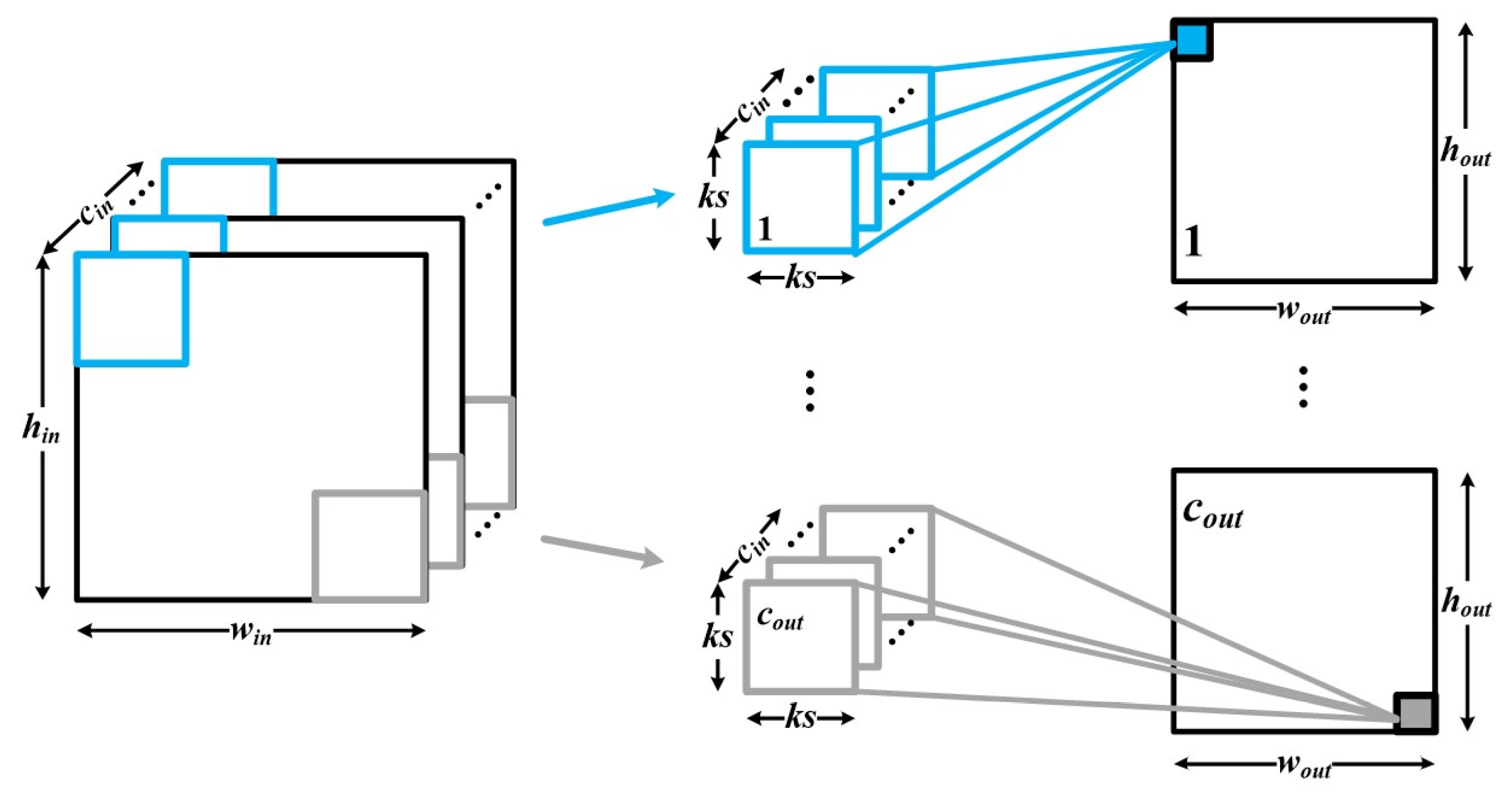
3. Proposed Parallelism Scheme

3.1. Proposed Parallelism Scheme of the BNN Accelerator

The proposed BNN accelerator adaptively applies two parallelism schemes according to the architectures of the target layer to offer high throughput in all layers. Our adaptive parallelism scheme consists of a combination of fmap-level parallelism and an advanced method that can efficiently cope with certain CONV layers that fmap-level parallelism cannot handle with 100% utilization. To minimize resource requirements, the proposed BNN accelerator is designed to operate with two parallelism schemes while using a similar data path as in conventional architectures with fmap-level parallelism. In addition, the proposed BNN accelerator is designed to make efficient use of the memory bandwidth allowed in various SoC platforms by using the design parameter P h w , which is the maximum number of operations that can be processed in one clock cycle. In other words, if P h w is set according to the memory bandwidth allowed in each SoC, our architecture can load P h w -size data in one clock cycle.
The first parallelism scheme (i.e., the advanced method) shown in Figure 2 is implemented for the initial layers, which have a small number of channels. The data scheduling of this scheme loads and processes k s × P c i n data bits per cycle, where k s is the kernel size and P c i n is the number of fmaps that can be loaded and processed in one clock cycle. Figure 3 shows how CONV layers are reorganized in the first parallelism mode, where i c and o c mean the number of input and output channels, respectively. The loops are reordered differently than in conventional BNN loops, bringing a kernel width loop and an input fmap loop to the innermost position. These inner loops are computed in the proposed BNN accelerator in one clock cycle. The in/out fmap loops split into an inner loop (computing units on processing elements; P c i n for input and P h w for output fmaps) and an outer loop (cycling iterations on network control unit; c i n / P c i n for input and c o u t / P h w for output fmaps). This scheme can efficiently cope with certain CONV layers in which utilization is drastically degraded when using fmap-level parallelism, as detailed in Section 3.2.2.
The second parallelism scheme used in the proposed BNNs accelerator is described in Figure 4 and Figure 5. Similar to fmap-level parallelism, this scheme loads and processes data on a per-channel basis, and it can achieve 100% utilization at deeper layers exceeding a certain number of input channels. An overview of this parallelism scheme is shown in Figure 5. The kernel width loop is moved outward, and the hardwired inner loop in the accelerator is only focused on the fmap channels. The parallelism parameter P h w is used to define the number of simultaneous XNOR operations in the processing elements (PEs) per cycle. In other words, P h w input fmap channels can be loaded and processed in one clock cycle. Therefore, the data scheduling of this scheme handles more channels per cycle than other schemes in deeper layers.
The proposed BNN accelerator executes one of the two parallelism schemes depending on the target layer as follows:
m t = 0 , c i n < P h w 1 , c i n P h w ,
where m t is the parallelism mode at the current target layer. The accelerator performs each parallelism scheme according to the value m t , as shown in Table 1. Considering that the processor is designed with P h w = 256 , if it targets a layer with respective c i n and k s values of 128 and three, the first parallelism is used, and the accelerator attains 75% utilization. This is a utilization improvement of 25% compared with the 50% attained via fmap-level parallelism. In contrast, if c i n is 256 or more, the proposed accelerator operates based on the second parallelism scheme, which can achieve 100% utilization.

3.2. Simulation Results

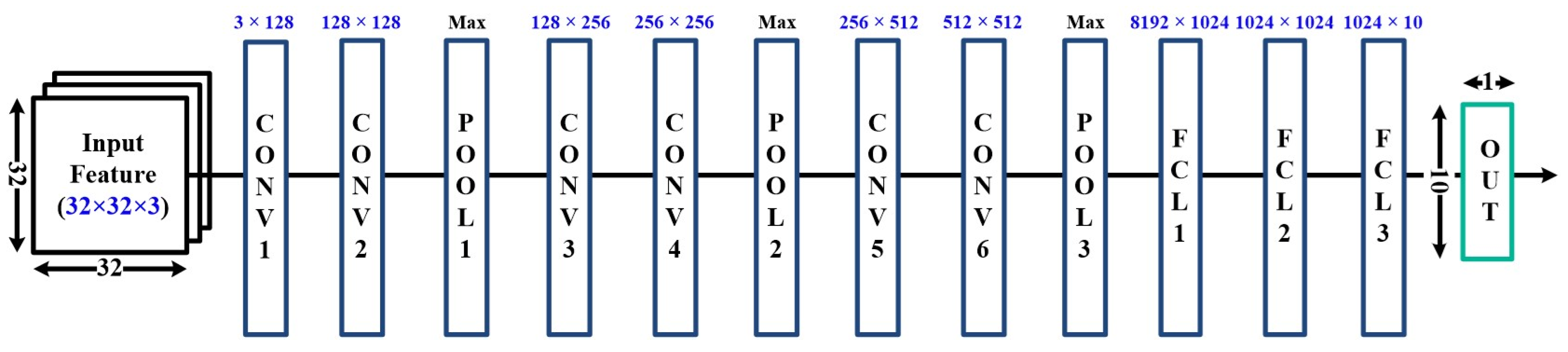
3.2.1. Target Network Topologies

To evaluate the efficiency of the proposed accelerator, common topologies of BNNs were used to make performance comparisons [20], as listed in Table 2. The architectures are described layer-by-layer using our own notation. Here, 2C128 and 2FC1024 refer to two CONV layers and two FC layers, with 128 and 1024 output channels, respectively. All max pooling (MP) layers have a size of 2 × 2 and a stride of two. The first topology is the original BNN described by Courbariaux et al. [16] and is referred to as BNN-Cifar10 in this paper. It is a variation of the VGG-11 topology with six CONV layers and three FC layers, as shown in Figure 6, and was used on the CIFAR-10 datasets. The CIFAR-10 dataset consists of 60,000 32 × 32 photos and contains 10 different classes, six different animals and four different vehicles. BNN-Cifar10 delivers state-of-the-art accuracy on the CIFAR-10 dataset. The second topology used for evaluation is the well-known VGG-16 model for the ImageNet dataset. The ImageNet dataset consists of 1.2 million images and contains 1000 different classes.

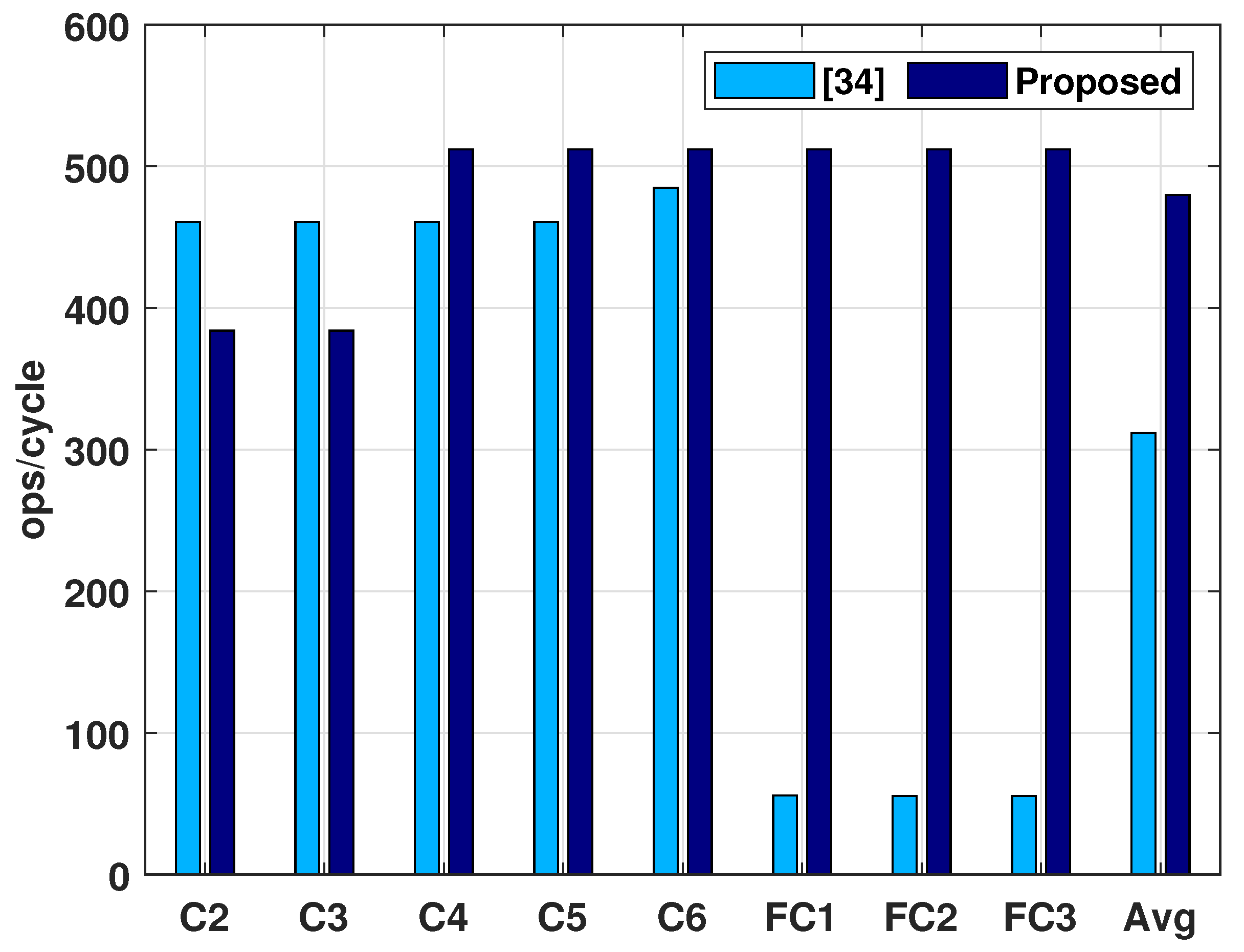
3.2.2. Performance Evaluation Results

We used operations per cycle (ops/cycle) to compare the throughput performance of our accelerator with that of existing BNN architectures. This parameter refers to the number of operations the accelerator can process per clock cycle, and we counted XNOR and popcount as separate operations [37]. In addition, ops/cycle can also represent the memory access efficiency because the number of operations that can be processed in each cycle is related to the number of data that can be loaded from memory in each cycle. To evaluate performance, we compared efficient BNN layer accelerators targeted for a low-power microcontroller [34,35,36,37,38]. To make a fair comparison, a similar number of operators (XNOR gates and adders for popcounts) were assumed for each accelerator. In addition, the first layer, whose fmaps are normally floating-point image data, was excluded in the comparison.
First, our architecture was assumed to have P h w = 256, and Reference [34] assumed having a similar number of operators (252). Moreover, Reference [34] adopted filter-level parallelism, which significantly degrades throughput performance in deeper layers, as shown in Figure 7. Although the work in [34] showed excellent peak performance (Gops/s, giga operations per second), it used more resources than the proposed accelerators, as detailed in Section 4.2.1, and the throughput decreased in other layers because it applied an inflexible parallelism scheme. The proposed parallelism can provide higher throughput performance in almost all layers (C4∼FC3), as shown in Figure 7. In addition, when comparing at 150 MHz, which was the operating frequency of the work in [34], the proposed accelerator operates with a lower latency of 1.57 ms for BNN-Cifar10 and of 30.92 ms for VGG-16 compared with [34].
On the other hand, the XNOR neural engine (XNE) [37] uses fmap-level parallelism to achieve 100% efficiency in the deeper layers, but its performance decreases sharply in the upper CONV layers, as shown in Figure 8. Our architecture and XNE were assumed to have P h w = 256 to make a fair comparison. The proposed accelerator can achieve on average ops/cycle 51.2 higher than XNE for VGG-16 and 32 higher for BNN-Cifar10. In addition, it can process with a lower latency of 1.96 ms for BNN-Cifar10 and 120.42 ms for VGG-16 compared with XNE when operating at a clock frequency of 300 MHz, which is the operating frequency of [37].

4. Design and Implementation Results

4.1. Hardware Architecture

Figure 9 shows the block diagram of the proposed BNN accelerator, including a network control unit (NCU), processing elements (PEs), a popcount unit (PCU), an accumulator, an activation unit, and a pooling unit. The PEs are composed of XNOR gates, AND gates, and a sub-popcount unit for processing 8 bit words. The feature vector that is input from the system is stored in a feature register for reuse. This feature vector is multiplied by the weight stream by the P h w XNOR gates in the PEs. To allow the proposed processor to operate with a smaller number of input features than P h w , the product vector is masked by sum filter coefficients, in an array of AND gates.
A popcount unit based on a simple combinational circuit is used to count the number of “1s” in the unmasked vector. Each PE has a sub-popcount unit for 8 bit words, from which a 4 bit output that ranges from zero to eight is extracted. These output components are merged in the main popcount unit. The final count is accumulated with the output of the current register in the accumulator. The accumulator consists of adder and P h w registers, and each register stores one output computed in a full accumulation cycle. The accumulated values are binarized in the activation unit with the thresholding phase defined in (3). This simple comparison involves batch normalization and binarization, as mentioned in Section 2.1. The max pooling of binarized values is computed using OR logical operations in the pooling unit when a target layer has a pooling phase. Otherwise, the binarized values bypass the pooling unit for flexibility.
The NCU is designed to execute the proposed parallelism schemes. It has R/Wregisters for loading the parameters of the target layer (e.g., c o u t , h o u t , w o u t , k s , etc.), a simple finite-state machine (FSM) to iterate the loop execution, and address calculators. The main FSM orchestrates the operation of the proposed accelerator and communicates with the micro-controller unit (MCU). By analyzing the layer parameters and selecting an appropriate parallelism scheme, the NCU controls the data loading phase and generates a memory address. It loads the data until the operation required for the current operation is completed, and the intermediate results during each iteration are stored in the accumulator. After these phases are completed, the threshold values from (3) are loaded and compared with the accumulated values in the activation unit. Then, the final outputs are streamed out to the bus interface.

4.2. Implementation Results

4.2.1. FPGA Implementation Results

The proposed BNN accelerator was designed using the Verilog hardware Description Language (HDL) and implemented on an XCZU7EV FPGA targeting the Xilinx ZYNQ Ultrascale+ ZCU-104 evaluation board. The proposed architecture with P h w = 256 requires 1050 configurable logic blocks (CLBs), 4816 CLB LUTs, and 2 DSPs, as shown in Table 3. In addition, the accelerator with the proposed parallelism schemes can process at an operating frequency of 371.6 MHz. To evaluate the efficiency of our architecture, we compared it with previous BNN implementations targeted at FPGA devices [34,35]. As shown in Table 3, although the proposed accelerator exhibits a lower peak performance than previous designs, it offers higher efficiency in terms of area (Gops/s/KLUT, Gops/s/KCLB) and power (Gops/s/W). The accelerators with filter-level parallelism [34,35] require more resources than the proposed accelerator because they need to store the previous row data and integer-scale intermediate values of the popcount operation.

4.2.2. VLSI Implementation Results

The proposed BNN accelerator was also synthesized to gate-level circuits using a 40 nm CMOS standard cell library. The key features of the proposed BNN accelerator are summarized in Table 4. It can be seen that the proposed architecture requires 23.37 K logic gates with a total die size of 0.016 mm 2 . This system can operate at an operating frequency of 450 MHz, and real-time processing is possible. To evaluate the efficiency of our architecture, we compared it with XNE [37] and XNORBIN [30], which represent the VLSI implementation results for the BNNs. To make a fair comparison, our architecture and XNE were assumed to have P h w = 128, and we normalized the area as:
A n o r m = A r e a ( T e c h / 40 nm ) 2 ,
where T e c h is the process technology expressed in nanometers [39]. As shown in Table 4, the proposed accelerator exhibited an average area-speed efficiency (Gops/s/ A n o r m ) 24% higher than XNE with fmap-level parallelism when operating at 300 MHz. In addition, our architecture can offer an area-speed efficiency 3.77 times higher than XNORBIN, which presents the streaming accelerator.

5. Conclusions

In this paper, we proposed a reconfigurable BNN accelerator with an adaptive parallelism scheme. Existing BNN layer accelerators suffer from throughput performance degradation at certain layers in BNN topologies because of their constant data scheduling schemes. On the other hand, streaming architectures, which provide parallelism schemes optimized for each layer, require a large amount of resources and are thus not suitable for edge devices. To overcome such problems, the proposed accelerator analyzes target layer parameters and performs operations with optimal parallelism using reasonable resources. The proposed parallelism schemes consist of fmap-level parallelism combined with an advanced method, which can efficiently cope with certain layers that fmap-level parallelism cannot handle with 100% utilization. In our performance evaluation for state-of-the-art BNN topologies, accelerators with the proposed parallelism schemes showed good throughput performance in terms of ops/cycle and low latency compared with existing BNN accelerators. The proposed processor was implemented with 1050 CLBs, 4816 CLB LUTs, and two DSPs on a Xilinx XCZU7EV FPGA device. It offered an area-speed efficiency 9.69 times higher than previous FPGA implementations for BNNs. In addition, it had a logic gate count of 23.37 K with a die size of 0.016 mm 2 , and it offered an area-speed efficiency 24% higher than existing VLSI implementations when operating at 300 MHz.

Author Contributions

J.C. designed the accelerator, performed the simulation and experiment, and wrote the paper. Y.J. (Yongchul Jung) and S.L. implemented the processor and revision of this manuscript. Y.J. (Yunho Jung) conceived of and led the research, analyzed the experimental results, and wrote the paper. All authors read and agreed to the published version of the manuscript.

Funding

This research received no external funding.

Acknowledgments

This work was supported by the Institute of Information & communications Technology Planning & Evaluation (IITP) grant funded by the Korean government (MSIT) (No. 2019-0-00056, 2020-0-00201), and the CAD tools were supported by IDEC.

Conflicts of Interest

The authors declare no conflict of interest.

References

  1. Jiao, L.; Zhao, J. A Survey on the New Generation of Deep Learning in Image Processing. IEEE Access 2019, 7, 172231–172263. [Google Scholar] [CrossRef]
  2. Alom, M.; Tha, T.; Yakopcic, C.; Westberg, S.; Sidike, P.; Nasrin, M.; Hasan, M.; Essen, B.; Awwal, A.; Asari, V. A State-of-the-Art Survey on Deep Learning Theory and Architectures. Electronics 2019, 8, 292. [Google Scholar] [CrossRef] [Green Version]
  3. Hu, R.; Peng, Z.; Ma, J.; Li, W. CNN-Based Vehicle Target Recognition with Residual Compensation for Circular SAR Imaging. Electronics 2020, 9, 555. [Google Scholar] [CrossRef] [Green Version]
  4. He, K.; Zhang, X.; Ren, S.; Sun, J. Deep Residual Learning for Image Recognition. In Proceedings of the IEEE Conference on Computer Vision and Pattern Recognition (CVPR), Las Vegas, NV, USA, 27–30 June 2016; pp. 770–778. [Google Scholar]
  5. Simonyan, K.; Zisserman, A. Very Deep Convolutional Networks for Large-Scale Image Recognition. arXiv 2014, arXiv:1409.1556. [Google Scholar]
  6. Sze, V.; Chen, Y.; Yang, T.; Ember, J. Efficient Processing of Deep Neural Networks: A Tutorial and Survey. Proc. IEEE 2017, 105, 2295–2329. [Google Scholar] [CrossRef] [Green Version]
  7. Zhou, S.; Wu, Y.; Ni, Z.; Zhou, X.; Wen, H.; Zou, Y. DoReFa-Net: Training Low Bitwidth Convolutional Neural Networks with Low Bitwidth Gradients. arXiv 2016, arXiv:1606.06160. [Google Scholar]
  8. Cho, J.; Jung, Y.C.; Lee, S.; Jung, Y.H. VLSI Implementation of Restricted Coulomb Energy Neural Network with Improved Learning Scheme. Electronics 2019, 8, 563. [Google Scholar] [CrossRef] [Green Version]
  9. Zhou, A.; Yao, A.; Guo, Y.; Xu, L.; Chen, Y. Incremental Network Quantization: Towards Lossless CNNs with Low-Precision Weights. arXiv 2017, arXiv:1702.03044. [Google Scholar]
  10. Lee, E.H.; Miyashita, D.; Chai, E.; Murmann, B.; Wong, S. LogNet: Energy-efficient neural networks using logarithmic computation. In Proceedings of the IEEE ICASSP, New Orleans, LA, USA, 5–9 March 2017; pp. 5900–5904. [Google Scholar]
  11. Li, F.; Zhang, B.; Liu, B. Ternary Weight Networks. In Proceedings of the NIPS Workshop Efficient Methods Deep Neural Networks, Barcelona, Spain, 8 December 2016. [Google Scholar]
  12. Jiao, L.; Luo, C.; Cao, W.; Zhou, X.; Wang, L. Accelerating Low bit-width Convolutional Neural Networks with Embedded FPGA. In Proceedings of the 2017 27th International Conference on Field Programmable Logic and Applications (FPL), Ghent, Belgium, 4–8 September 2017. [Google Scholar]
  13. Vita, A.D.; Pau, D.; Benedetto, L.D.; Rubino, A.; Petro, F.; Licciardo, G.D. Low Power Tiny Binary Neural Network with improved accuracy in Human Recognition Systems. In Proceedings of the 2020 23rd Euromicro Conference on Digital System Design (DSD), Kranj, Slovenia, 26–28 August 2020. [Google Scholar]
  14. Vita, A.D.; Russo, A.; Pau, D.; Benedetto, L.D.; Rubino, A.; Licciardo, G.D. A Partially Binarized Hybrid Neural Network System for Low-Power and Resource Constrained Human Activity Recognition. IEEE Trans. CAS 1 2020, 67, 3893–3904. [Google Scholar]
  15. Courbariaux, M.; Bengio, Y.; David, J. BinaryConnect: Training Deep Neural Networks with Binary Weights during propagations. In Proceedings of the NIPS, Montreal, QC, Canada, 7–12 December 2015. [Google Scholar]
  16. Courbariaux, M.; Hubara, I.; Soudry, D.; EI-Yaniv, R.; Bengio, Y. Binarized Neural Networks: Training Deep Neural Networks with Weights and Activations Constrained to +1 or -1. arXiv 2016, arXiv:1602.02830. [Google Scholar]
  17. Rastegary, M.; Ordonez, V.; Redon, J.; Farhadi, A. XNOR-Net: ImageNet Classification Using Binary Convolutional Neural Networks. arXiv 2016, arXiv:1603.05279. [Google Scholar]
  18. Lin, X.; Zhao, C.; Pan, W. Towards Accurate Binary Convolutional Neural Networks. In Proceedings of the Advances in Neural Information Processing Systems, Long Beach, CA, USA, 4–9 December 2017. [Google Scholar]
  19. Darabi, S.; Belbahri, M.; Courbariaux, M.; Nia, V.P. BNN+: Improved Binary Network Training. In Proceedings of the Learning Representations, Vancouver, BC, Canada, 30 April–3 May 2018; pp. 1–10. [Google Scholar]
  20. Simons, T.; Lee, D. A Review of Binarized Networks. Electronics 2019, 8, 661. [Google Scholar] [CrossRef] [Green Version]
  21. Bethge, J.; Bartz, C.; Yang, H.; Chen, Y.; Meinel, C. MeliusNet: Can Binary Neural Networks Achieve MobileNet-level Accuracy? arXiv 2020, arXiv:2001.05936. [Google Scholar]
  22. Umuroglu, Y.; Fraser, N.J.; Gambardella, G.; Blott, M.; Leong, P.; Jahre, M.; Vissers, K. FINN. In Proceedings of the ACM/SIGDA International Symposium on FPGA, Monterey, CA, USA, 22–24 February 2017; ACM Press: New York, NY, USA, 2017; pp. 65–74. [Google Scholar]
  23. BloTT, M.; Preuber, T.B.; Frased, N.J.; Gambardella, G.; O’brien, K.; Umuroglu, Y.; Leeser, M.; Vissers, K. FINN-R: An End-to-End Deep-Learning Framework for Fast Exploration of Quantized Neural Networks. ACM Trans. Reconfigurable Technol. Syst. 2018, 11, 1–23. [Google Scholar] [CrossRef]
  24. Fiscaletti, G.; Speziali, M.; Stornaiuolo, L.; Santambrogio, M.D.; Sciuto, D. BNNsplit: Binarized Neural Networks for Embedded Distributed FPGA-based Computing Systems. In Proceedings of the 2020 DATE, Grenoble, France, 9–13 March 2020; pp. 975–978. [Google Scholar]
  25. Nurvitadhi, E.; Sheffield, D.; Sim, J.; Mishra, A.; Venkatesh, G.; Marr, D. Accelerating Binarized Neural Networks: Comparison of FPGA, CPU, GPU, and ASIC. In Proceedings of the 2016 International Conference on Field-Programmable Technology (FPT), Xi’an, China, 7–9 December 2016; pp. 77–84. [Google Scholar]
  26. Liang, S.; Yin, S.; Liu, L.; Luk, W.; Wei, S. FP-BNN: Binarized Neural Network on FPGA. Neurocomputing 2012, 275, 1072–1086. [Google Scholar] [CrossRef]
  27. Fu, C.; Zhu, S.; Chen, H.; Koushanfar, F.; Su, H.; Zhao, J. SimBNN: A Similarity-Aware Binarized Neural Network Acceleration Framework. In Proceedings of the IEEE FCCM, San Diego, CA, USA, 28 April–1 May 2019; p. 319. [Google Scholar]
  28. Ghasemzadeh, M.; Samragh, M.; Koushanfar, F. ReBNet: Residual Binarized Neural Network. In Proceedings of the IEEE FCCM, Boulder, CO, USA, 29 April–1 May 2018; pp. 57–64. [Google Scholar]
  29. Geng, T.; Wang, T.; Wu, C.; Yang, C.; Song, S.; Li, A.; Herbordt, M. LP-BNN: Ultra-low-latency BNN Inference with Layer Parallelism. In Proceedings of the 2019 IEEE 30th International Conference on Application-specific Systems, Architectures and Processors (ASAP), New York, NY, USA, 15–17 July 2019; pp. 9–16. [Google Scholar]
  30. Bahou, A.A.; Karunaratne, G.; Andri, R.; Cavigelli, L.; Benini, L. XNORBIN: A 95 TOp/s/W Hardware Accelerator for Binary Convolutional Neural Networks. In Proceedings of the IEEE Symp. COOL CHIPS, Yokohama, Japan, 18–20 April 2018; pp. 1–3. [Google Scholar]
  31. Lin, J.; Xing, T.; Zhao, R.; Zhang, Z.; Srivastava, M.; Tu, Z.; Gupta, R.K. Binarized Convolutional Neural Networks with Separable Filters for Efficient Hardware Acceleration. In Proceedings of the IEEE CVPR, Honolulu, HI, USA, 21–26 July 2017; pp. 27–35. [Google Scholar]
  32. Wang, E.; Davis, J.J.; Cheung, P.Y.K.; Constantinides, G.A. LUTNet: Learning FPGA Configurations for Highly Efficient Neural Network Inference. IEEE Trans. Comput. 2020, 69, 1795–1808. [Google Scholar] [CrossRef] [Green Version]
  33. Lammie, C.; Xiang, W.; Azghadi, M.R. Training Progressively Binarizing Deep Networks using FPGAs. In Proceedings of the IEEE ISCAS, Sevilla, Spain, 12–14 October 2020; pp. 1–5. [Google Scholar]
  34. Yonekawa, H.; Nakahara, H. On-Chip Memory Based Binarized Convolutional Deep Neural Network Applying Batch Normalization Free Technique on an FPGA. In Proceedings of the IEEE IPDPSW, Orlando, FL, USA, 29 May–2 June 2017; pp. 98–105. [Google Scholar]
  35. Gu, P.; Ma, H.; Chen, R.; Li, P.; Xie, S.; Wang, D. FBNA: A Fully Binarized Neural Network Accelerator. In Proceedings of the 2018 28th International Conference on Field Programmable Logic and Applications (FPL), Dublin, Ireland, 27–31 August 2018; pp. 51–54. [Google Scholar]
  36. Zhou, Y.; Redkar, S.; Huang, X. Deep Learning Binary Neural Network on an FPGA. In Proceedings of the IEEE MWSCAS, Boston, MA, USA, 6–9 August 2017; pp. 281–284. [Google Scholar]
  37. Conti, F.; Schiavone, D.; Benini, L. XNOR Neural Engine: A Hardware Accelerator IP for 21.6fj/op Binary Neural Network Inference. IEEE Trans. CAD 2018, 37, 2940–2951. [Google Scholar] [CrossRef] [Green Version]
  38. Rusci, M.; Cavigelli, L.; Benini, L. Design Automation for Binarized Neural Networks: A Quantum Leap Opportunity? In Proceedings of the IEEE ISCAS, Florence, Italy, 27–30 May 2018. [Google Scholar]
  39. Jung, Y.C.; Cho, J.; Lee, S.; Jung, Y.H. Area-Efficient Pipelined FFT Processor for Zero-Padded Signals. Electronics 2019, 8, 1397. [Google Scholar] [CrossRef] [Green Version]
Figure 1. High-dimensional convolutions in CNNs.
Electronics 10 00230 g001
Figure 2. Data scheduling example of the first parallelism scheme.
Electronics 10 00230 g002
Figure 3. BNN layers’ loop for the first parallelism scheme; the loops highlighted in light yellow are computed in one clock cycle.
Electronics 10 00230 g003
Figure 4. Data scheduling example of the second parallelism scheme.
Electronics 10 00230 g004
Figure 5. BNN layers’ loop for the second parallelism scheme; the loops highlighted in light yellow are computed in one clock cycle.
Electronics 10 00230 g005
Figure 6. Topology of the BNN designed for CIFAR-10.
Electronics 10 00230 g006
Figure 7. Comparison results of throughput performance for BNN-Cifar10. ops, operations.
Electronics 10 00230 g007
Figure 8. Comparison results of throughput performance for VGG-16. XNE, XNOR neural engine.
Electronics 10 00230 g008
Figure 9. Block diagram of the proposed BNN accelerator.
Electronics 10 00230 g009
Table 1. Supported parallelism schemes based on m t of the proposed BNN accelerator.
ModeParallelism Scheme
m t = 0First scheme introduced in Figure 2
m t = 1Second scheme shown in Figure 4
Table 2. Architectures of the network topologies used to evaluate performance. MP, max pooling; C, CONV.
NetworkArchitectureDatasetAccuracy
BNN-Cifar102C128-MP-2C256-MP-2C512-MP-2FC1024-FC10CIFAR-1089.95%
VGG-162C64-MP-2C128-MP-3C256-MP-3C512-MP-3C512-MP-2FC4096-FC1000ImageNet75.5%
Table 3. Comparison of the FPGA implementation results of our accelerator with previous works. CLB, configurable logic block.
[34] [35]Proposed ( P h w = 256)
FPGAXCZU9EGXC7Z020XCZU7EV
Target NetworkVGG-16BNN-Cifar10VGG-16
ParallelismFilter-levelProposed
Operating Frequency150 MHz143 MHz371 MHz
CLB (Slice)47,946N.A.1050
LUTN.A.34.9 K4.8 K
DSP402
BRAM136710389
Peak Performance460.8 Gops/s722.8 Gops/s177.68 Gops/s
Area EfficiencyGops/s/KLUTN.A.2137.02
Gops/s/KCLB9.61N.A.169.22
Power Efficiency (Gops/s/W)20.94219250
Table 4. Comparison results of the VLSI implementations.
[30][37] Proposed ( P h w = 128)
Technology65 nm65 nm22 nm40 nm
Area (10 3 μ m 2 )54041.27.616.49
Normalized Area204.4915.6025.1216.49
Operating Frequency156 MHz300 MHz300 MHz
Peak Performance244 Gops/s66 Gops/s74 Gops/s
Area Efficiency (Gops/s/ A n o r m )1.194.232.634.49
Publisher’s Note: MDPI stays neutral with regard to jurisdictional claims in published maps and institutional affiliations.

