Article

Design and Implementation of a Farrow-Interpolator-Based Digital Front-End in LTE Receivers for Carrier Aggregation

1
Department of Electrical and Electronics Engineering, Konkuk University, Neungdong-ro 120, Gwangjin-gu, Seoul 05029, Korea
2
Department of Electronics Engineering, Pusan National University, 2, Busandaehak-ro 63beon-gil, Geumjeong-gu, Busan 46241, Korea
*
Author to whom correspondence should be addressed.
Electronics 2021, 10(3), 231; https://doi.org/10.3390/electronics10030231
Submission received: 27 December 2020 / Revised: 17 January 2021 / Accepted: 19 January 2021 / Published: 20 January 2021
(This article belongs to the Section Circuit and Signal Processing)

Abstract

:
A digital front-end decimation chain based on both Farrow interpolator for fractional sample-rate conversion and a digital mixer is proposed in order to comply with the long-term evolution standards in radio receivers with ten frequency modes. Design requirement specifications with adjacent channel selectivity, inband blockers, and narrowband blockers are all satisfied so that the proposed digital front-end is 3GPP-compliant. Furthermore, the proposed digital front-end addresses carrier aggregation in the standards via appropriate frequency translations. The digital front-end has a cascaded integrator comb filter prior to Farrow interpolator and also has a per-carrier carrier aggregation filter and channel selection filter following the digital mixer. A Farrow interpolator with an integrate-and-dump circuitry controlled by a condition signal is proposed and also a digital mixer with periodic reset to prevent phase error accumulation is proposed. From the standpoint of design methodology, three models are all developed for the overall digital front-end, namely, functional models, cycle-accurate models, and bit-accurate models. Performance is verified by means of the cycle-accurate model and subsequently, by means of a special C++ class, the bitwidths are minimized in a methodic manner for area minimization. For system-level performance verification, the orthogonal frequency division multiplexing receiver is also modeled. The critical path delay of each building block is analyzed and the spectral-domain view is obtained for each building block of the digital front-end circuitry. The proposed digital front-end circuitry is simulated, designed, and both synthesized in a 180 nm CMOS application-specific integrated circuit technology and implemented in the Xilinx XC6VLX550T field-programmable gate array (Xilinx, San Jose, CA, USA).

1. Introduction

The digital front-end (DFE) of a radio receiver is used to convert the sample rate of the analog-to-digital converter (ADC) and filter out the remaining interference after the radio frequency (RF) front-end filters serve the role of initial band and channel selection. The channel with the desired signal is sharply filtered by a chain of digital filters in the DFE and the required signal-to-noise ratio (SNR) is achieved by sufficiently rejecting various types of blockers. The filtered signal channel from the DFE in the radio chip is typically passed over to the digital baseband processor or modem chip and at the same time the sample rate is reduced from the high ADC sample rate to acceptable rates for the baseband processor by means of downsampling in the DFE circuitry. This is in contrast to what is accomplished in the radio transmitter where upsampling or sample rate multiplication is carried out in the interpolation chain. The DFE in the radio receiver is a decimation chain and a cascade of digital filters are used in the DFE to attain the desired output SNR in an effective manner, namely, rather than using one digital filter with an extraordinarily large number of filter taps, a series of multistage digital filters are employed to attain the required SNR in a successive manner, reducing the total number of taps [1].
A host of literature deals with the digital front-ends in the radio receivers for wireless communication. A multirate subsampling front-end incorporates programmable digital decimation stages to accommodate variable bit rates in a software radio receiver in [2]. The front-end consists of digital down-converters or down-conversion mixers, comb-type channel select filters with decimation, and accumulators. Direct digital frequency synthesizers control the channel select filters and the accumulators. An integer-factor sample-rate converter for software-defined radio receivers is simulated in [3]. Implementation efficiency is emphasized in the front stages by using a decimate-by-16 multiplier-free cascaded integrator comb filter while high performance is emphasized in the back stages by using a 3-stage decimator. In addition, an increasing hardware effort is needed as the sample rate (and thus the oversampling ratio) decreases down the decimation chain, favoring placing a fractional sample-rate converter in the front stages of the chain [4]. The importance of decimation filters will continue to expand, as the high-speed data from a fast analog-to-digital converter need to be downsampled prior to ingestion by a processor [5]. As another software-defined radio receiver, the implementation in [6] takes a discrete-time approach at the analog baseband prior to the analog-to-digital converter. A programmable fractional rate-change digital front-end for software-defined radio is designed in [7], which comprises cascaded integrator comb filters, half-band filters (for decimation by 2), finite-impulse-response (FIR) filters, and polyphaser filters with numerically controlled oscillators (for decimation by variable factors). A fractional sample-rate conversion filter for a software radio receiver is implemented in a field-programmable gate array in [8]. It is composed of numerically controlled oscillators (based on phase accumulators and coordinate rotation digital computers or CORDICs), mixers (based on CORDICs), cascaded integrator comb (CIC) filters, and Farrow filters.
The digital front-end in [9] uses several decimation and interpolation stages, which are implemented as polyphase filters. A channelizer that is well-suited to extracting multiple radio channels from a wideband input signal is simulated in [10] based on a reconfigurable filter bank. The filter bank is in turn based on decimation and interpolation. A tunable narrow-band digital front-end for delta-sigma ADCs is simulated in [11], which starts with a quadrature mixer followed by a complex mixer (with a tunable frequency) and a cascaded integrator comb decimator in between. A look-up table based numerically controlled oscillator is coupled with the mixers. The final stages are polyphase decimation filters. One of the structures that incorporate a tunable rate change factor in polyphase filters is the Farrow structure [4], which is amenable to time interpolation. A digital front-end for direct-sampling receivers is implemented in [12], where digital mixers, cascaded integrator comb filters, Taylor-series polynomial interpolation filters (based on resampling for fractional decimation), and decimation-by-2 filters are employed. In [13], a digital down-converter with polyphase cascaded integrator comb filters is simulated to validate its compatibility with the time interleaved analog-to-digital converter. Parallel processing is employed in the channelization for an IEEE 802.11ac receiver in [14], which is implemented in software on a graphics processing unit. A lower-error Farrow structured variable fractional delay interpolation is described and simulated in [15].
In this paper, a digital front-end decimation chain in radio receivers with fractional sample-rate conversion is proposed, simulated, designed, and implemented, which can fulfill carrier aggregation in the long-term evolution (LTE) and LTE-advanced (LTE-A) standards while accommodating multiple frequency bands. Fractional sample-rate conversion (FSRC) is realized by means of a Farrow interpolator and the output of the DFE is fed to the orthogonal frequency division multiplexing (OFDM) baseband processor. A methodic design methodology is taken to guarantee the register transfer level (RTL) performance relative to higher abstraction level performances and to accomplish the design goals on an overall OFDM receiver system basis. The proposed DFE architecture is fully compliant with the LTE-A CA specification and it is synthesized in an application-specific integrated circuit (ASIC) and also implemented in a field-programmable gate array (FPGA), which are also analyzed in depth in terms of performance and hardware complexity.
Prior to giving a more detailed look at the DFE architecture in Section 2, we first sketched the overall structure of the proposed DFE for LTE and LTE-A in Figure 1. The cascaded integrator comb (CIC) filter received the ADC output signal and converted the sampling rate by a factor of 1/N where N is an integer. FSRC is capable of converting the sample rate by a factor of L/M where L/M is a rational number, not only an integer number. The digital mixer (DM) removed the intermediate frequency (IF) of the component carriers in carrier aggregation (CA) for LTE-A and increased or decreased each carrier frequency. Subsequently, carrier aggregation filters (CAF1 and CAF2) adjusted the sample rate or sampling frequency to the output frequency of the LTE DFE receiver by a last-step conversion and eliminate unwanted frequency–domain interference arising from CA. Lastly, the channel selection filter (CSF) got rid of the residual interference while sustaining the desired signal.
The paper is organized as follows. The design flow and the overall DFE architecture are described in Section 2. The building blocks of the overall DFE architecture are elaborated on in terms of basic concept and theory in Section 3, which is subdivided into the explanation of CIC, FSRC, digital mixer, carrier aggregation filter, and channel selection filter. Simulated results of the overall DFE architecture is detailed in Section 4. The detailed hardware implementation and the experimental results of the proposed DFE in both an ASIC and an FPGA are demonstrated in Section 5, together with some discussion, which are followed by the conclusion.

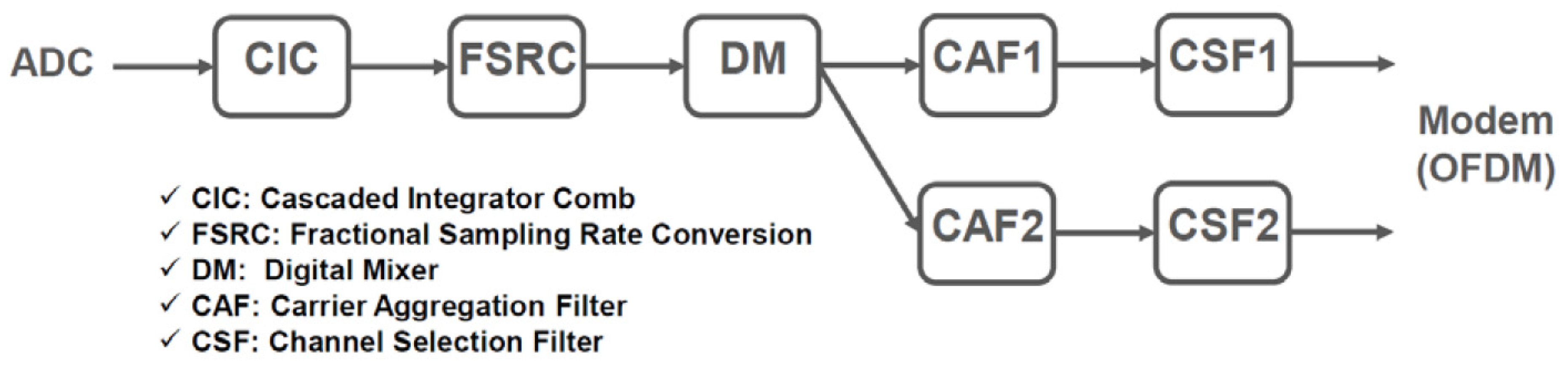
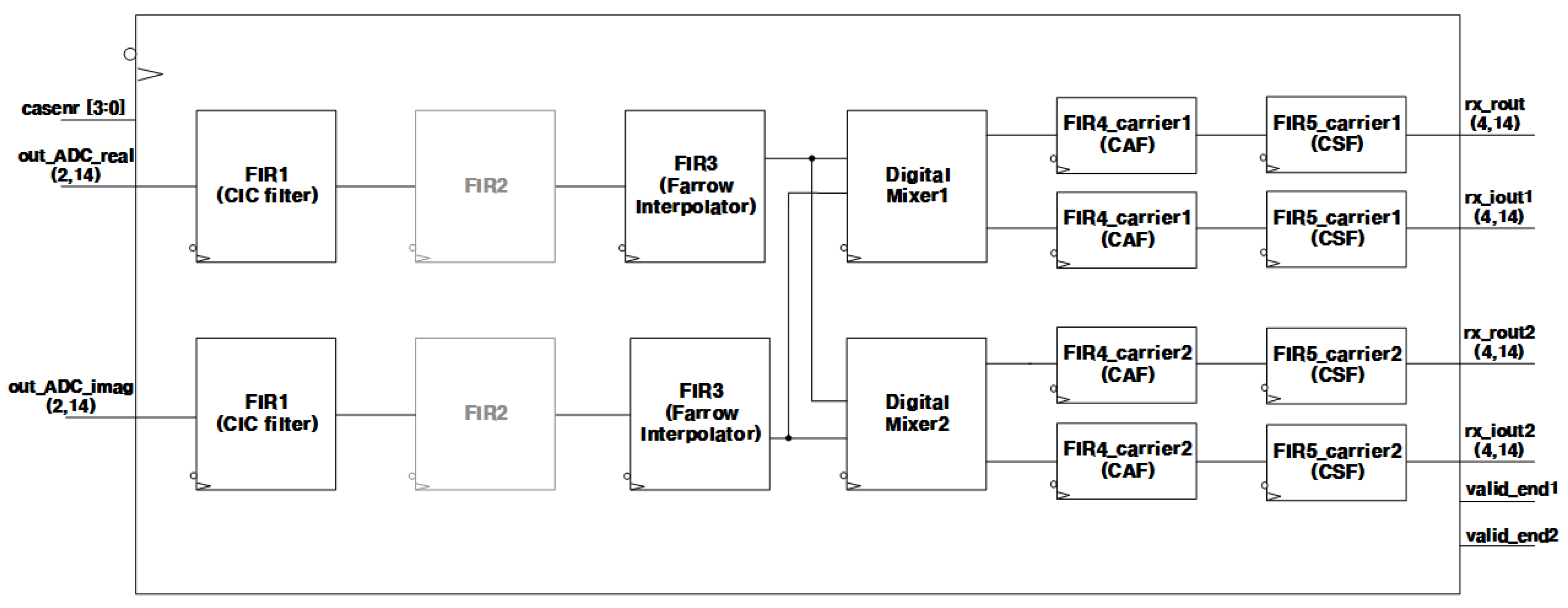
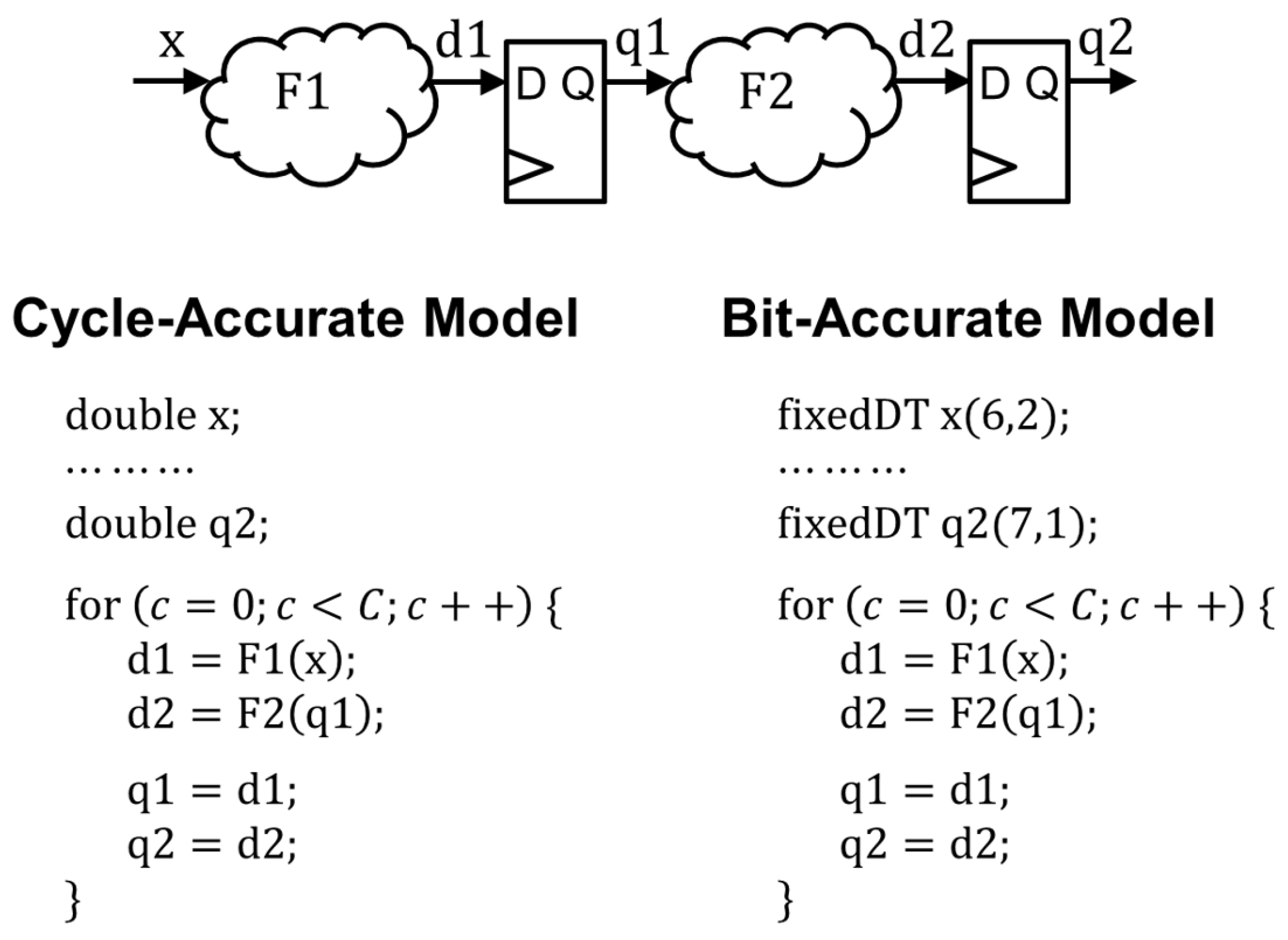
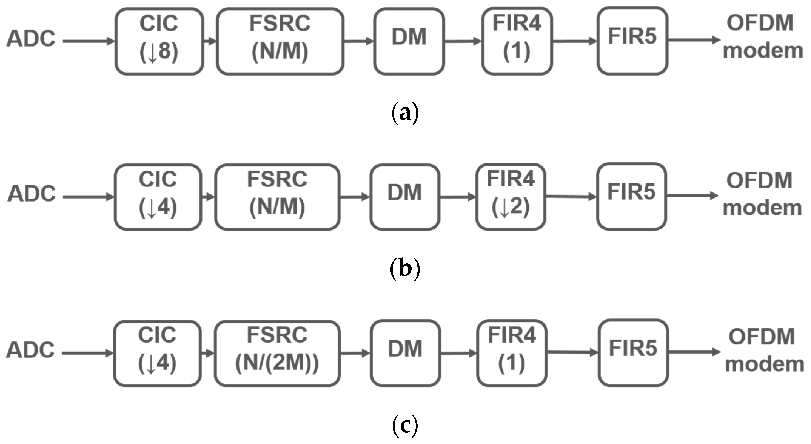
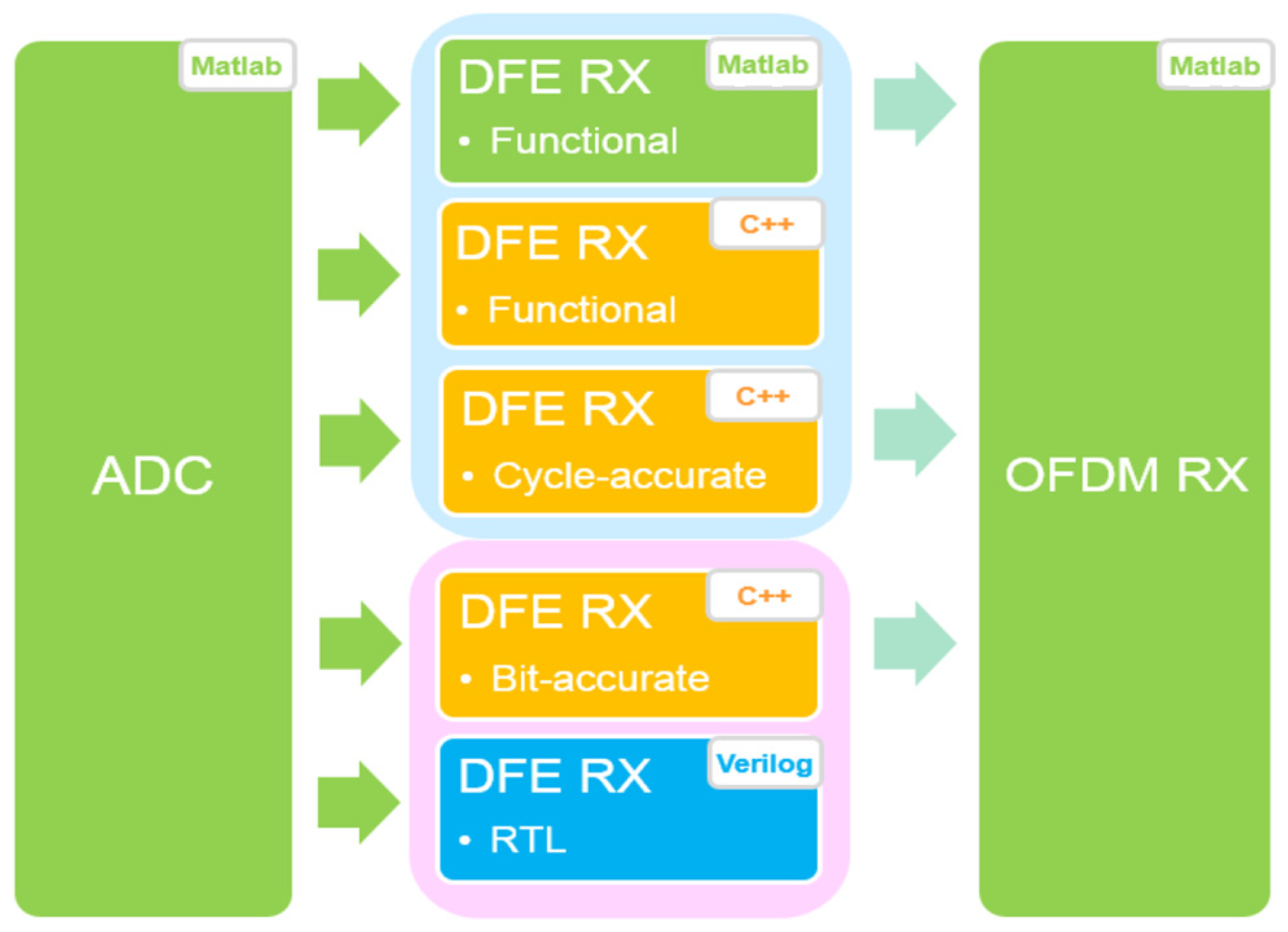
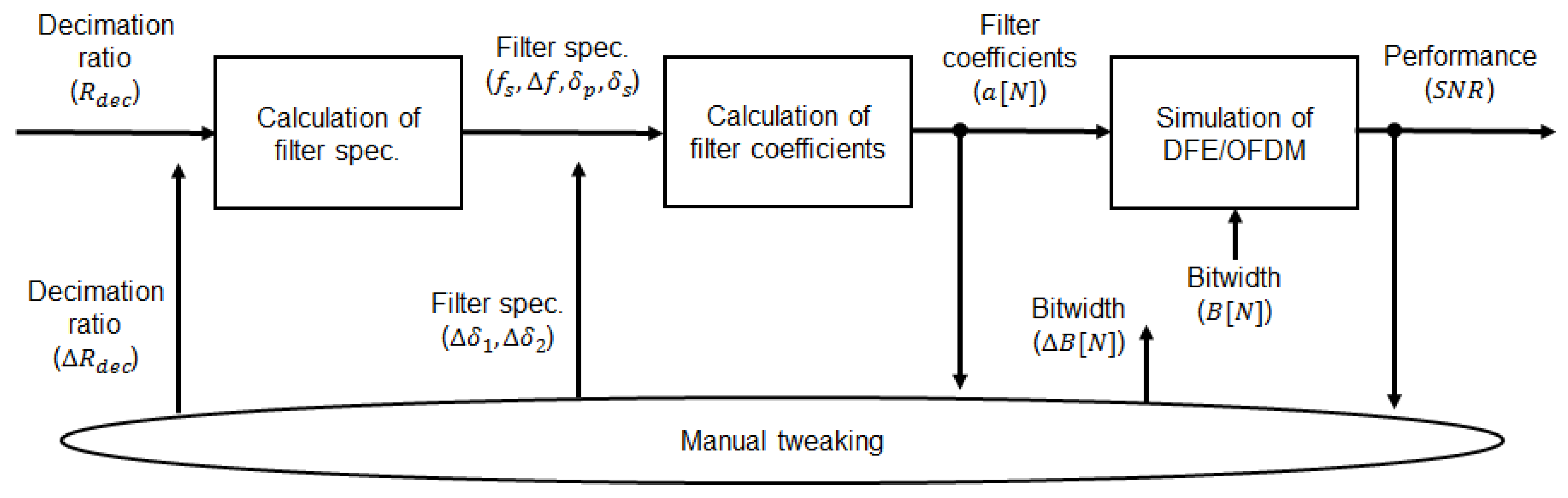
2. Design Flow and the Overall DFE Architecture

The design flow taken for the DFE targeted at LTE CA is diagrammed in Figure 2. The input of the DFE for LTE CA, modeled in Matlab, comes in from the ADC. The OFDM receiver (RX) was also modeled in Matlab. In the beginning, the output of the ADC is fed to the DFE Matlab model whose output is given to the OFDM receiver model, from which the error performance of the DFE functional model is obtained. After the error performance satisfies the design requirement specification, the DFE C++ functional model is constructed, which fulfills the same behavior as the DFE Matlab functional model. The discrepancy between the output of the Matlab model and that of the C++ model is made to be less than −200 dB. The cycle-accurate model of the DFE is constructed subsequently, where the hardware architecture is taken into account, namely, the model closely mimics the hardware behavior, but the quantization is not applied yet. The deviation of the output of the cycle-accurate model from that of the C++ functional model is also rendered less than −200 dB. Next, the bit-accurate model is constructed, which also closely resembles the hardware behavior and furthermore applies quantization that occurs in digital hardware. The bit-accurate DFE model is fed with the input and the resulting output is applied to the OFDM receiver model, from which the error performance is obtained. The word length and hardware structures are varied to meet the required performance. Finally, the HDL DFE model is constructed such that the model behaves exactly the same as the bit-accurate model, leading to the same output and zero error. The error performance is verified up front in the bit-accurate model phase and hence the Verilog HDL model is synthesized and optimized to meet the other requirements, namely, speed and area.
A signal path of the DFE for LTE CA consists of FIR1 (CIC filter), FIR3 (Farrow interpolator) [16], digital mixer, FIR4 (carrier aggregation filter or CAF), and FIR5 (channel selection filter or CSF), as exhibited in Figure 3. In order to process both the in-phase and quadrature signals, a pair of CIC filters and Farrow interpolators are employed [17]. A pair of digital mixers is used to facilitate CA. A quad of carrier aggregation filters and channel selection filters exist to accommodate in-phase and quadrature signals and two carriers (carrier1 and carrier 2) in CA. FIR2 shown as a shaded box in Figure 3 may serve as an antidrooping filter in an attempt to partly cancel the drooping in the CIC filter and Farrow interpolator, which is not necessary in the current version.
An RF phase-locked loop (PLL) reference clock can be set to 26 MHz, 39 MHz, 45.5 MHz, and 52 MHz for the overall DFE in Figure 3 and an active-low synchronous reset was used to initialize the register values. The mode select signal, casenr, determines which frequency mode was adopted for the LTE DFE. Ten frequency modes or cases of 20 MHz, 15 MHz, 10 MHz, 5 MHz, 3 MHz, 1.4 MHz, 20 MHz + 20 MHz (CA), 20 MHz + 15 MHz (CA), 20 MHz + 10 MHz (CA), and 5 MHz + 5 MHz (CA) were supported. The ADC outputs, out_ADC_real and out_ADC_imag, were fed to the DFE circuitry as the in-phase and quadrature inputs, respectively. (2, 14) after out_ADC_real, for instance, denotes 2 integer bits and 14 fractional bits. Four outputs, in-phase and quadrature outputs for carrier1 and carrier2, exist for the four CSFs. Two auxiliary outputs, valid_end1 and valid_end2, of the DFE exist to represent the timing of the carrier1 and carrier2 outputs. Specifically, if one of the auxiliary outputs is high, the in-phase and quadrature outputs of carrier1 are regarded as valid. Likewise, if the other auxiliary output is high, the in-phase and quadrature outputs of carrier2 are deemed valid. If a FIFO memory or shift register is present at the output of the DFE, the output values can be stored in sequence according to the timing of the output frequency (30.72 MHz), by using the auxiliary output set to high as an indicator.

3. Building Blocks of the Overall DFE Architecture

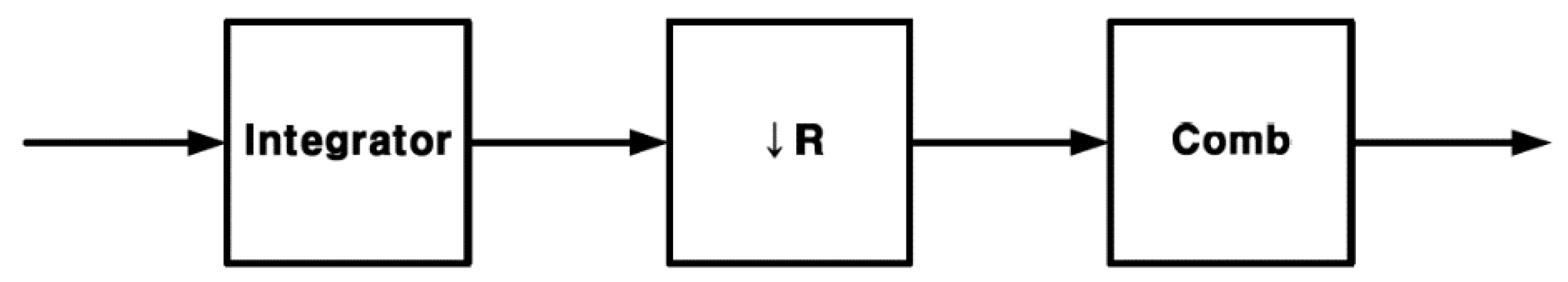
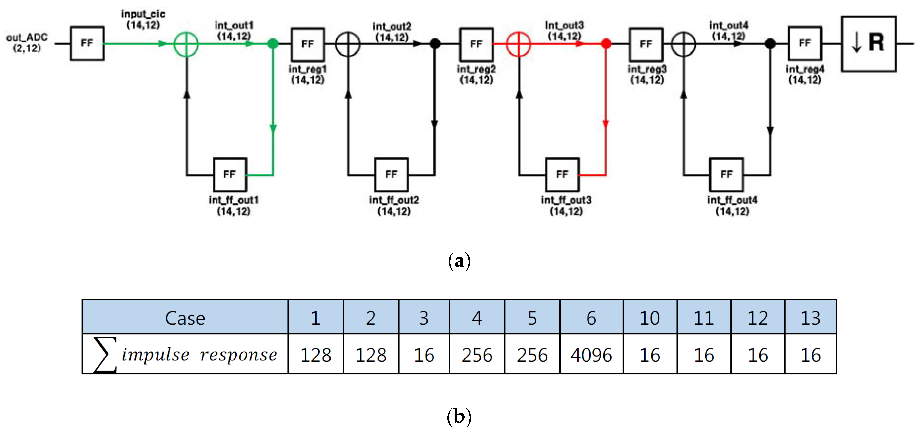
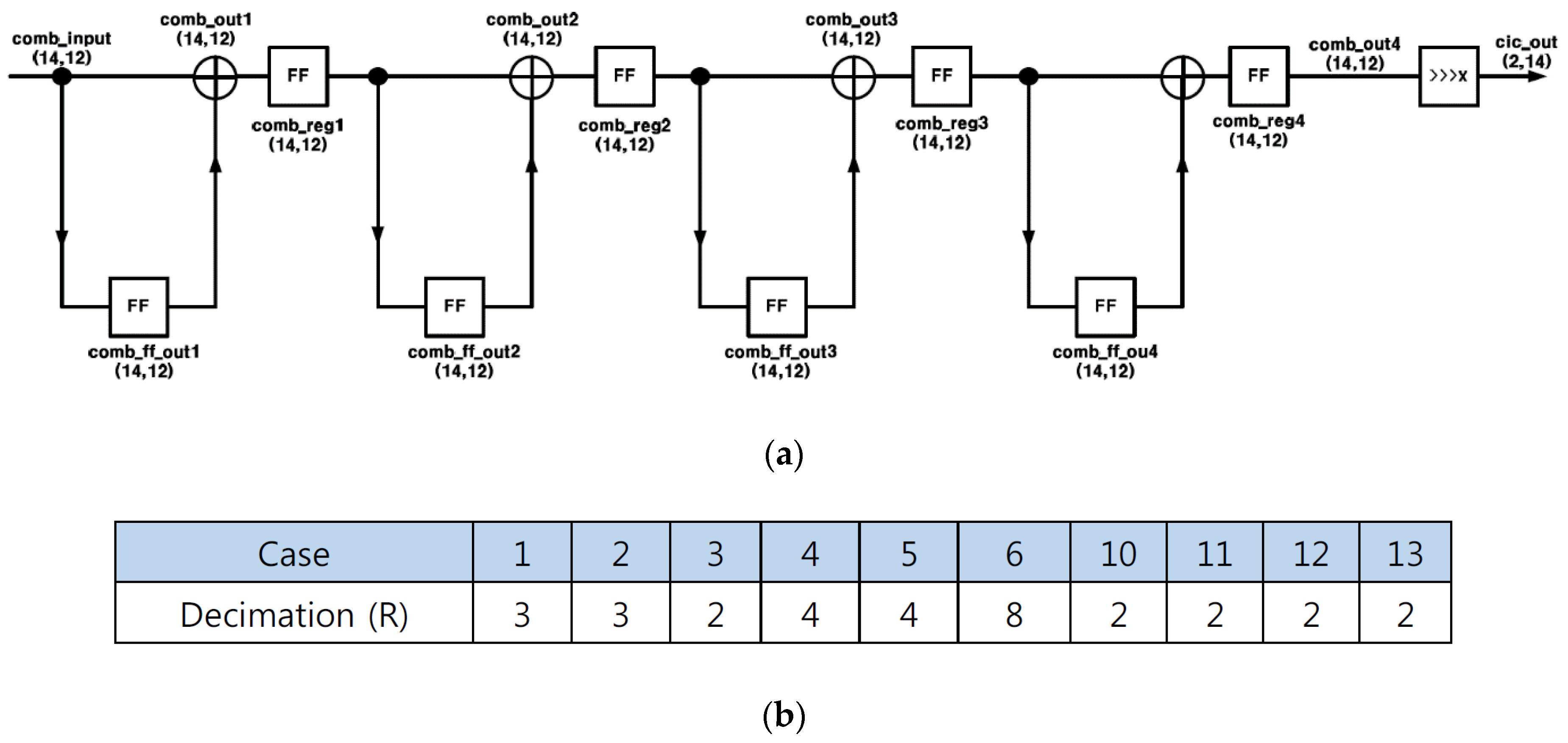
3.1. FIR1 (CIC Filter)

The CIC filter [18] (FIR1) illustrated in Figure 4 dispenses with the multiplier and appears to have a regular structure. It leads to a reduced amount of computation and hence is amenable to high-speed and low-power implementation of decimation and interpolation filters. It is used as the first block of our DFE, namely, immediately after the ADC, which operates at a higher frequency than the latter blocks. As shown in Figure 4, the CIC filter comprises the integrator, the decimator (or downsampler), and the comb filter, where the integrator actually consists of a cascade of N unit integrators.
The transfer function of the integrator and decimator is expressed as Equation (1), where R is the decimation factor and D is the differential delay of the comb filter.
H I n t e g r a t o r ( z ) = ( D R 1 1 z 1 ) N
The transfer function of the comb filter is affected by the downsampler and equated to Equation (2).
H C o m b ( z ) = ( 1 z   D R ) N
The transfer function of the overall CIC filter is expressed as Equation (3).
H C I C ( z ) = H I n t e g r a t o r ( z ) H C o m b ( z ) = ( D R 1 z   D R 1 z 1 ) N
From these equations, the CIC filter is identified to have the structure in Figure 5, where each small square represents the D-type flip-flop (FF). Figure 6 shows the output of the ADC (left) and the output of the FIR1 (CIC filter).
FIR1 (CIC filter) is designed as follows. Ten cases or frequency modes for the LTE DFE have different parameter values for FIR1. The CIC filter order, N, is set to 4 for all the cases while the differential delay of the comb filter, D, can have different values of 3, 2, 4, or 8 for different cases. The downsample rate R is set to be identical to D in each case and hence noble identity [19] implementation is possible, yielding high-speed operation and low-power drain in the comb filter, as shown in Figure 7.

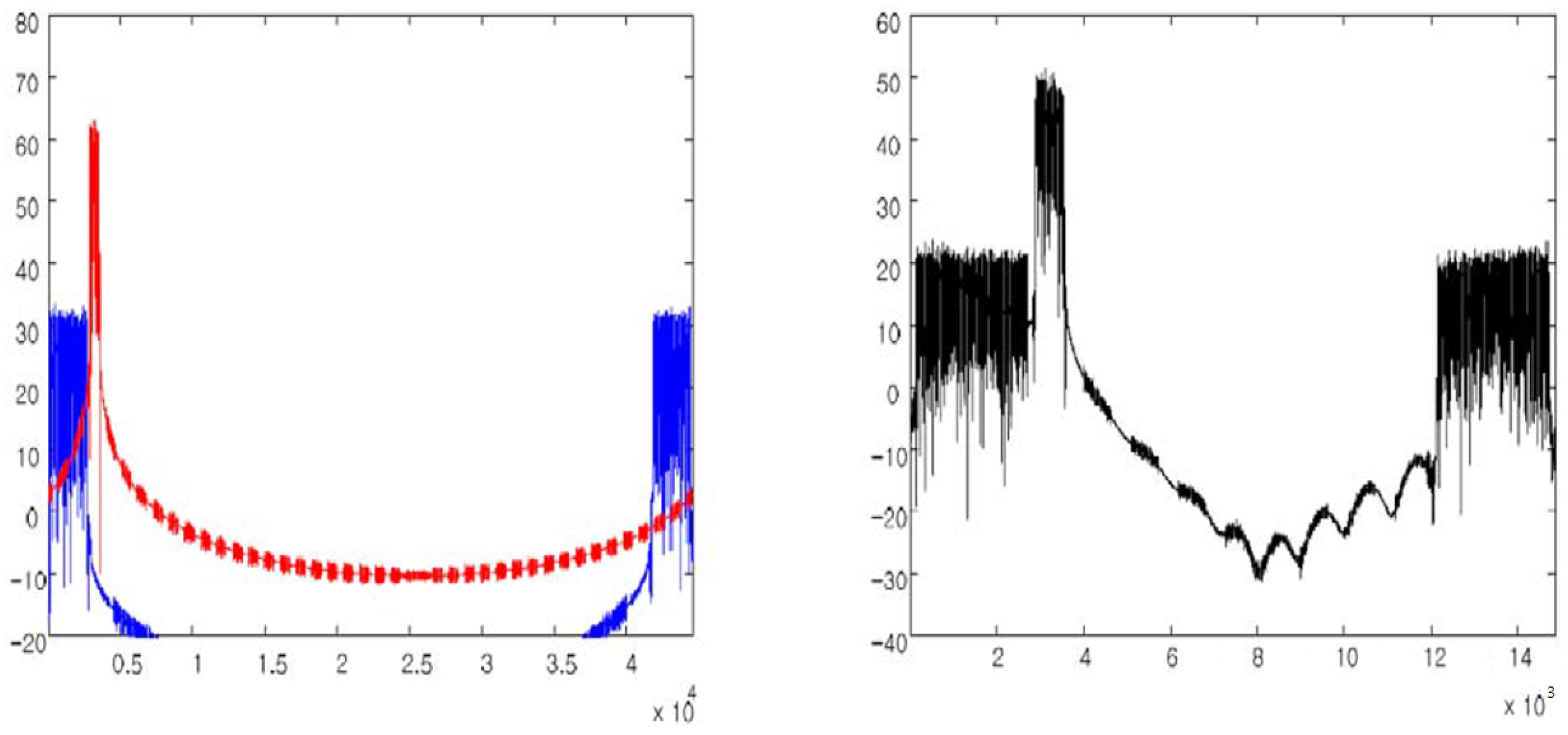
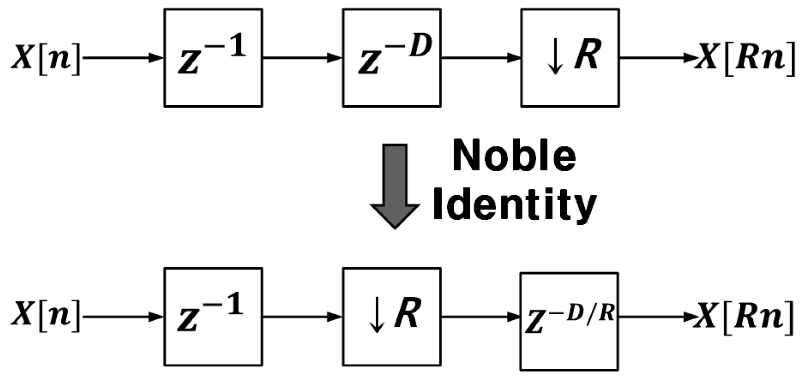
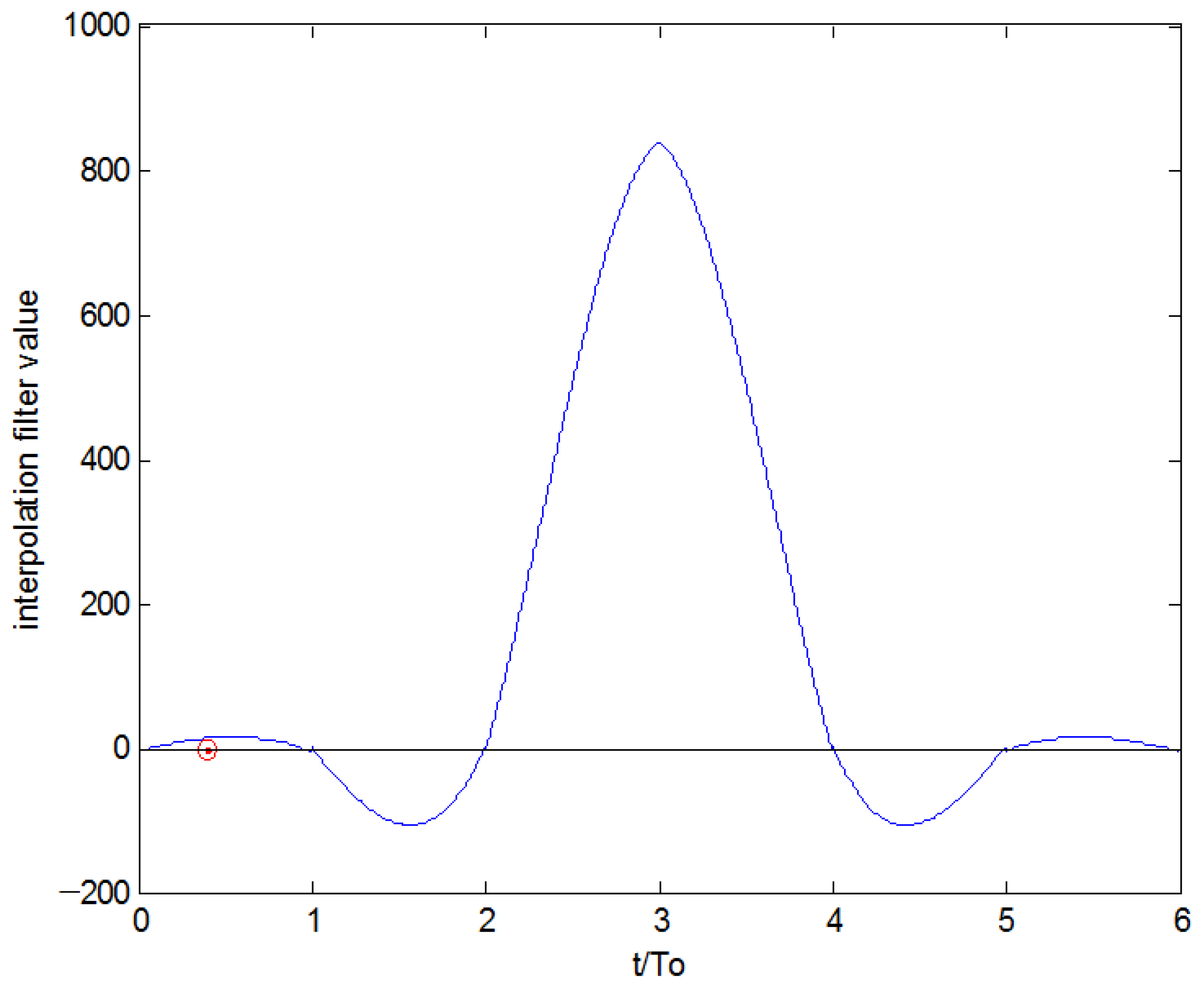
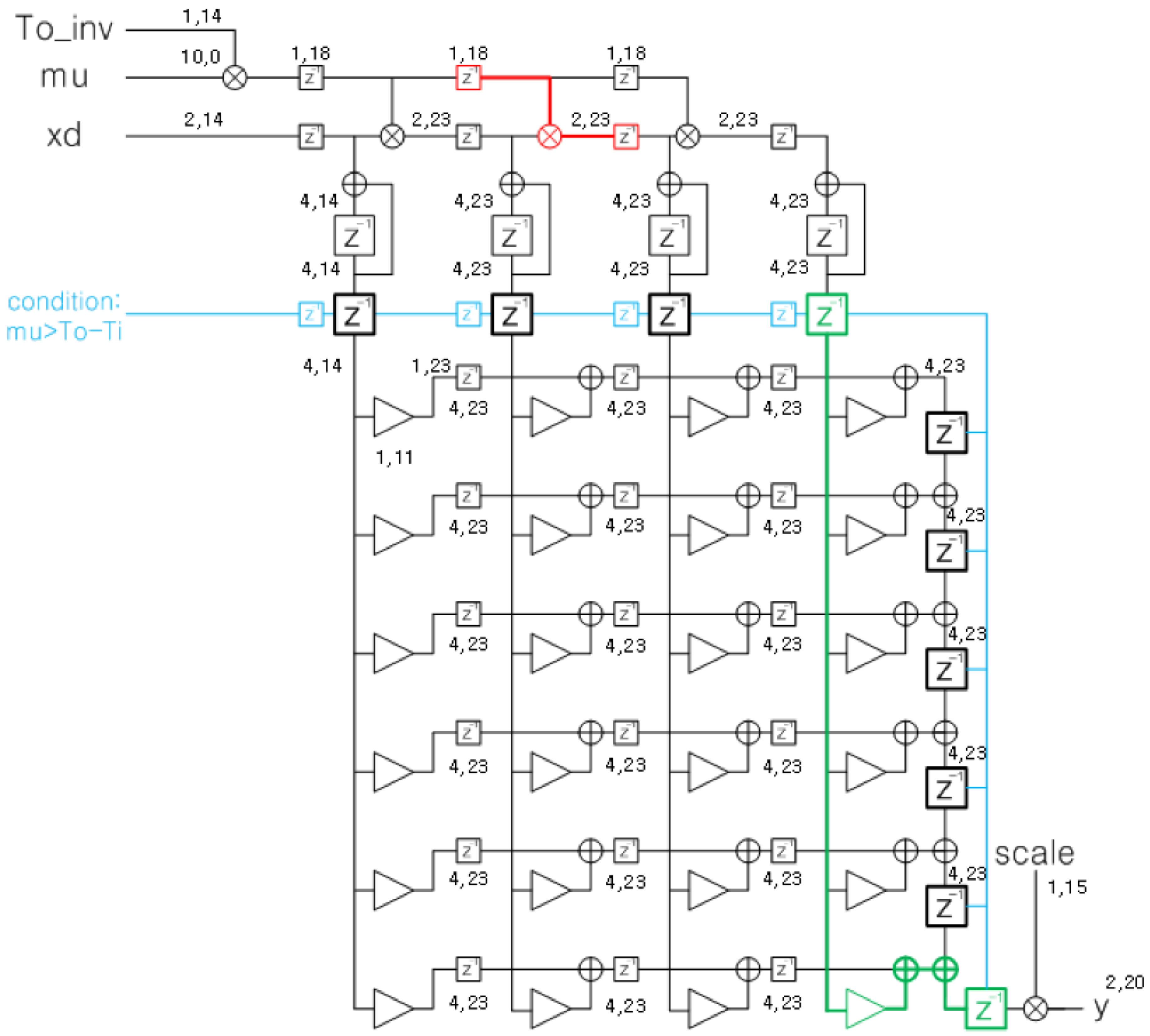
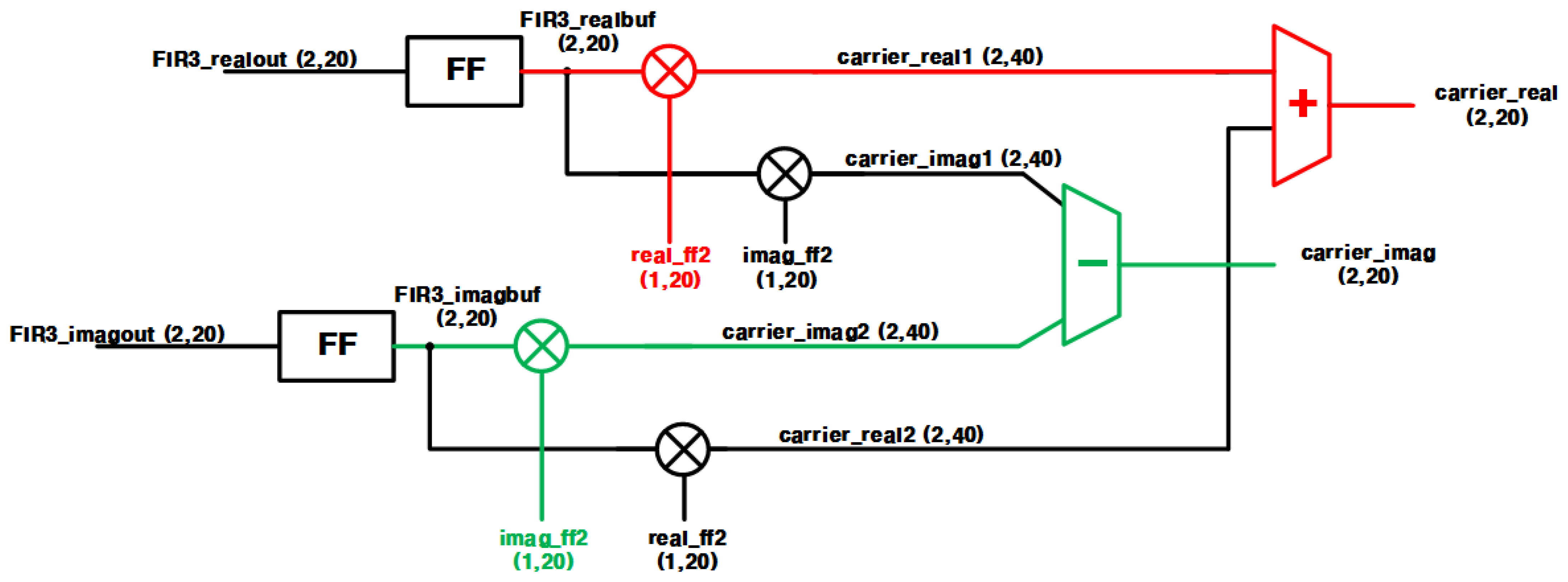
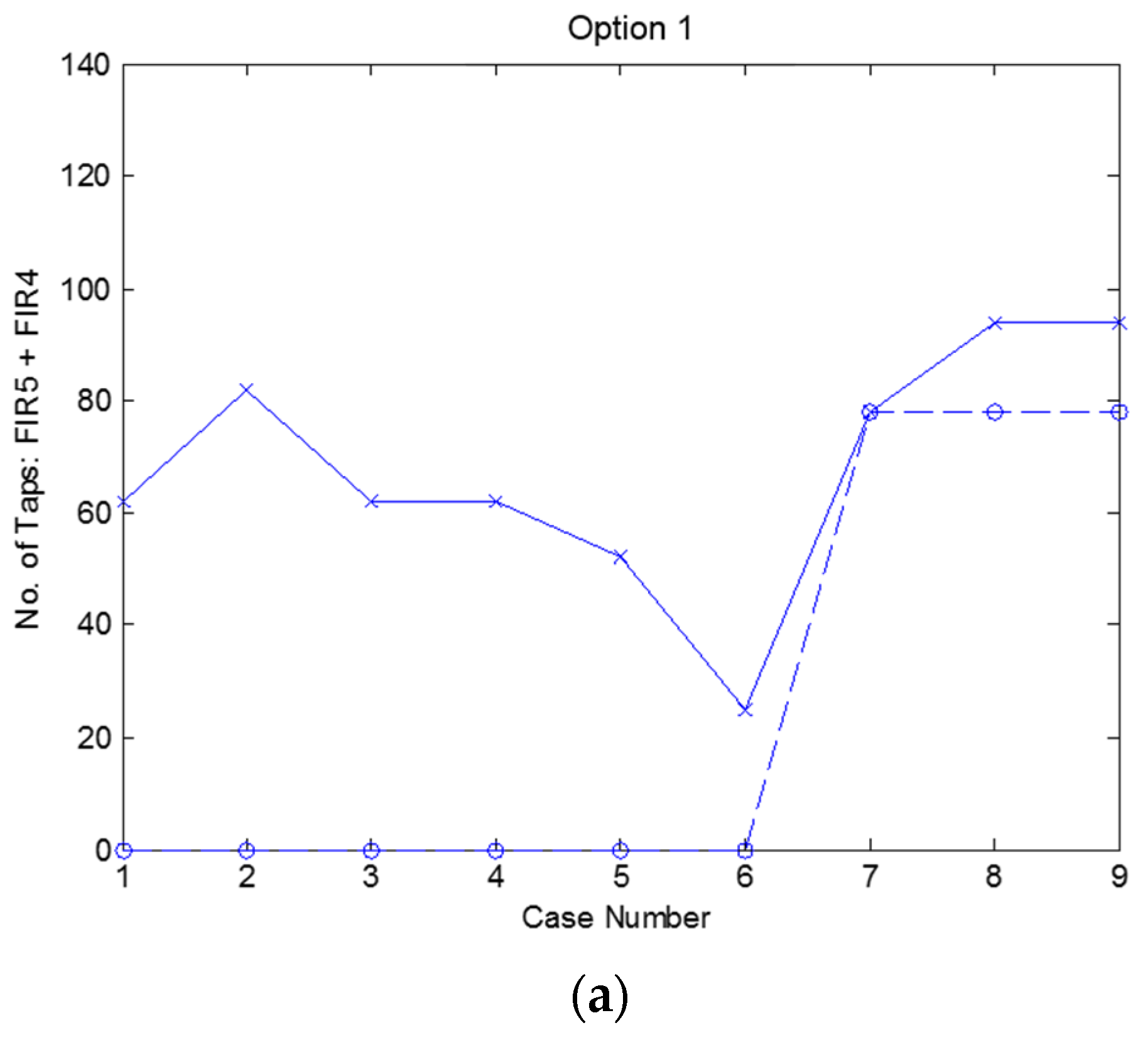
3.2. FIR3 (Farrow Interpolator)

FIR3 (Farrow interpolator) plays the part of converting the sample rate by a fractional or rational number. For LTE DFE, two decimation factors, 128/325 and 192/325, were employed. In Figure 8, the two signals far apart became near to each other after decimation by the Farrow interpolator, during which filtering was also carried out to prevent aliasing. Basically, to convert the sample rate by a rational factor N/M, an upsampling or interpolation by a factor of N was followed by a downsampling by M, leading to a significantly large number of filter coefficients. Farrow interpolator in LTE DFE enables fractional sample-rate conversion with a small number of coefficients by making use of polynomial operation explained in the following.
In the process of sample-rate conversion by a rational number, interpolation [20] is needed in the Farrow interpolator to obtain new values that did not exist in the input, as illustrated in Figure 9 where the light green lines correspond to hI in Equation (4) and red marks represent the interpolated values obtained from the sum over hI values at that x coordinate. Equation (4) represents discrete-time interpolation [21,22], where Ti is the input sample period and To is the output sample period.
y ( k T i ) = m x ( m T i )   h I ( k T i m T o )
Equation (4) is rearranged as Equations (5)–(7), subsequently.
y ( k T i ) = m = m k I 2 m k I 1 x ( m T i )   h I ( k T o m T i )
y ( k T i ) = i = I 1 I 2 x ( ( m k i ) T i )   h I ( k T o ( m k i ) T i )
y ( k T i ) = i = I 1 I 2 x ( ( m k i ) T i )   h I ( ( k T o T i m k + i ) T i )
where i = int[kTo/Ti] − m and mk = int[kTo/Ti], where int[R] is the maximum integer, which is smaller than or equal to the real number R. Further rearranged, Equation (7) is represented as Equation (8).
y ( k T i ) = y [ ( m k + μ k ) T i ] = i = I 1 I 2 x ( ( m k i ) T i )   h I ( ( i μ k ) T i )
where μk = kTo/Timk and 0 ≤ μk < 1. In FIR3 (Farrow interpolator) for LTE DFE, hI ((iμk)Ti) was modeled as a cubic polynomial in μk, which was readily calculated. An interpolation filter corresponding to Farrow interpolator was formulated below in Matlab. The elements in farrow_matrix represent the cubic polynomial coefficients that are identically used for hardware implementation.
  • frac_delay = 1/325:1/325:1;
  • for i = 1:length(frac_delay),
  • farrow_matrix = [−4 96 −128 32;
  • 3 −558 820 −264;
  • 839 −166 −1340 664;
  • −3 854 652 −664;
  • 1 −290 28 264;
  • −4 64 −32 −32];
  • mu=frac_delay(i);
  • interp_coefs(i,:) = flipud(farrow_matrix) * [mu.^(0:3)]’;
  • end;
  • hinterp=reshape(interp_coefs,[],1);
  • plot(0:1/325:6 − 1/325,hinterp);
  • hold on,plot(128/325,hinterp(129),‘or’);
  • xlabel(‘t/To’);
  • ylabel(‘interpolation filter value’).
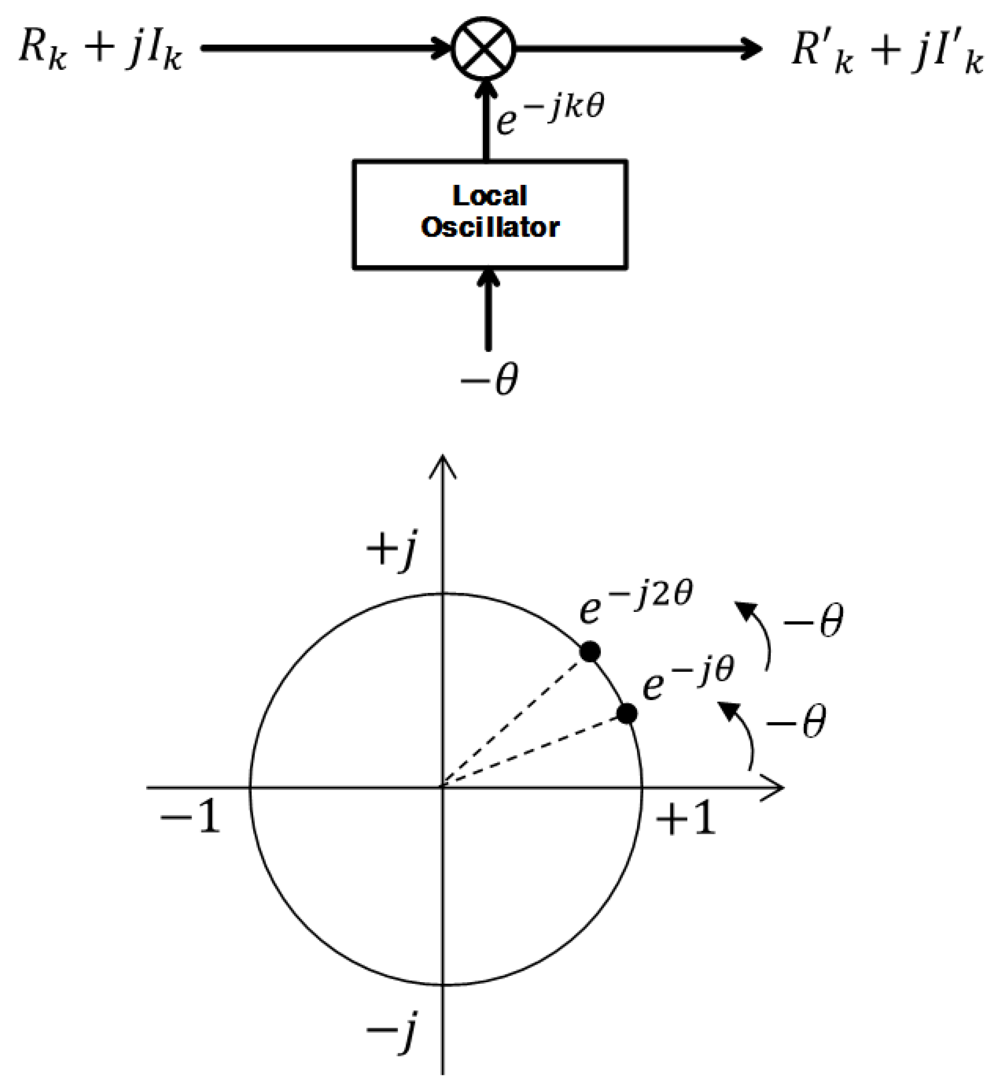
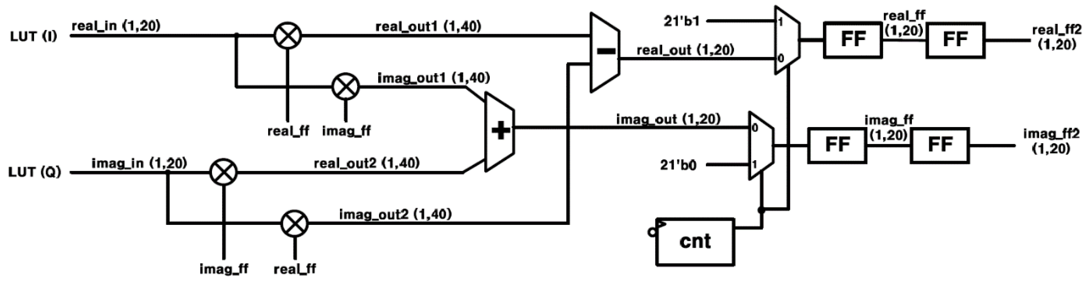
Figure 10 represents the continuous-time impulse response of the Farrow interpolator. Since the x coordinate denotes t/To, the impulse response length is 6To. The y coordinate denotes the value of the interpolation filter before normalization. The small red circle indicates the point where t = Ti and hence the interval between t = 0 and t = Ti corresponds to the Farrow interpolator input period.

3.3. Digital Mixer

The digital mixer removes the IF of each carrier and translates each carrier frequency by using an angle applied externally, as plotted in Figure 11. The local oscillator outputs consecutively accumulated values for a certain angle. The angle information that the local oscillator needs to operate on can be initialized by referencing the look-up table (LUT) in which the I (in-phase) and Q (quadrature) initial values were stored, according to which case of the ten cases was assumed. The exponential value from the local oscillator was obtained by operating on the accumulated angle each clock cycle. This value and the FIR3 (Farrow interpolator) output were the inputs to the complex multiplier from which the final output of the digital mixer was obtained.
Figure 12 illustrates how the digital mixer behaves when it receives the output from FIR3, assuming case 10 (+10 MHz, −10 MHz) is selected for LTE CA. Carrier 1 output is shifted to the minus direction (leftward) relative to the input while carrier 2 output is shifted to the plus direction (rightward) relative to the input. The amounts of frequency translation in the digital mixer are (carrier 1, carrier 2) = (−10 MHz, +10 MHz), (−10 MHz, +7.5 MHz), (−10 MHz, +5 MHz), and (−5 MHz, +5 MHz) for cases 10, 11, 12, and 13, respectively, while bypassed for cases 1–6.

3.4. FIR4 (Carrier Aggregation Filter)

The role of FIR4 (carrier aggregation filter), for the sake of a given carrier, is to remove the other carrier originating from CA in the LTE. The left half of Figure 13 shows, for the LTE 20 MHz + 20 MHz case, carrier 1 and carrier 2 shifted by the mixer to the center frequency (namely, the origin in the x axis) and farther from the center frequency, respectively. This is the input to FIR4. To the right of carrier 1 exists an inband blocker and in about the middle of the graph exists carrier 2. The right half of Figure 13 displays the output of FIR4 that runs decimation by 2 such that the carrier 1 signal around the center frequency takes a broader seat while the carrier 2 signal in the middle is attenuated and the inband blocker power is more or less attenuated as well. To this end, low-pass filtering is needed. In other words, in the FIR4 filter, the signal adjacent to the center frequency is sustained while other signals than the desired carrier are attenuated, followed by downsampling through which the sample rate becomes identical to the output frequency.
The design of the digital FIR lowpass filter is derived from the analog lowpass filter prototype on the basis of impulse invariance. The attenuation at a specified frequency is expressed as a function of the order of the filter and the 3 dB frequency or the corner frequency, f3dB, as expressed in Equation (9). If the attenuation at a frequency of 2 MHz is required to be, for instance, −42 dB, from the standard specification, then a 3rd-order filter with a 3 dB frequency of 400 kHz can meet this requirement.
A t t e n u a t i o n = 10 × log 10 ( 1 + ( f f 3 d B ) 2 × o r d e r )
For all the 10 cases, FIR4 (CA filter) filter coefficients (carrier 1 and carrier 2) were obtained. All the coefficients were symmetric and the total numbers of coefficients were 1, 1, 14, 14, 22, and 18 and 14, 9, 30, and 30 for cases 1–6 and 10–13, respectively, in the case of carrier 1. In the case of carrier 2, the total numbers of coefficients were 14, 9, 30, and 30 for cases 10–13, respectively.

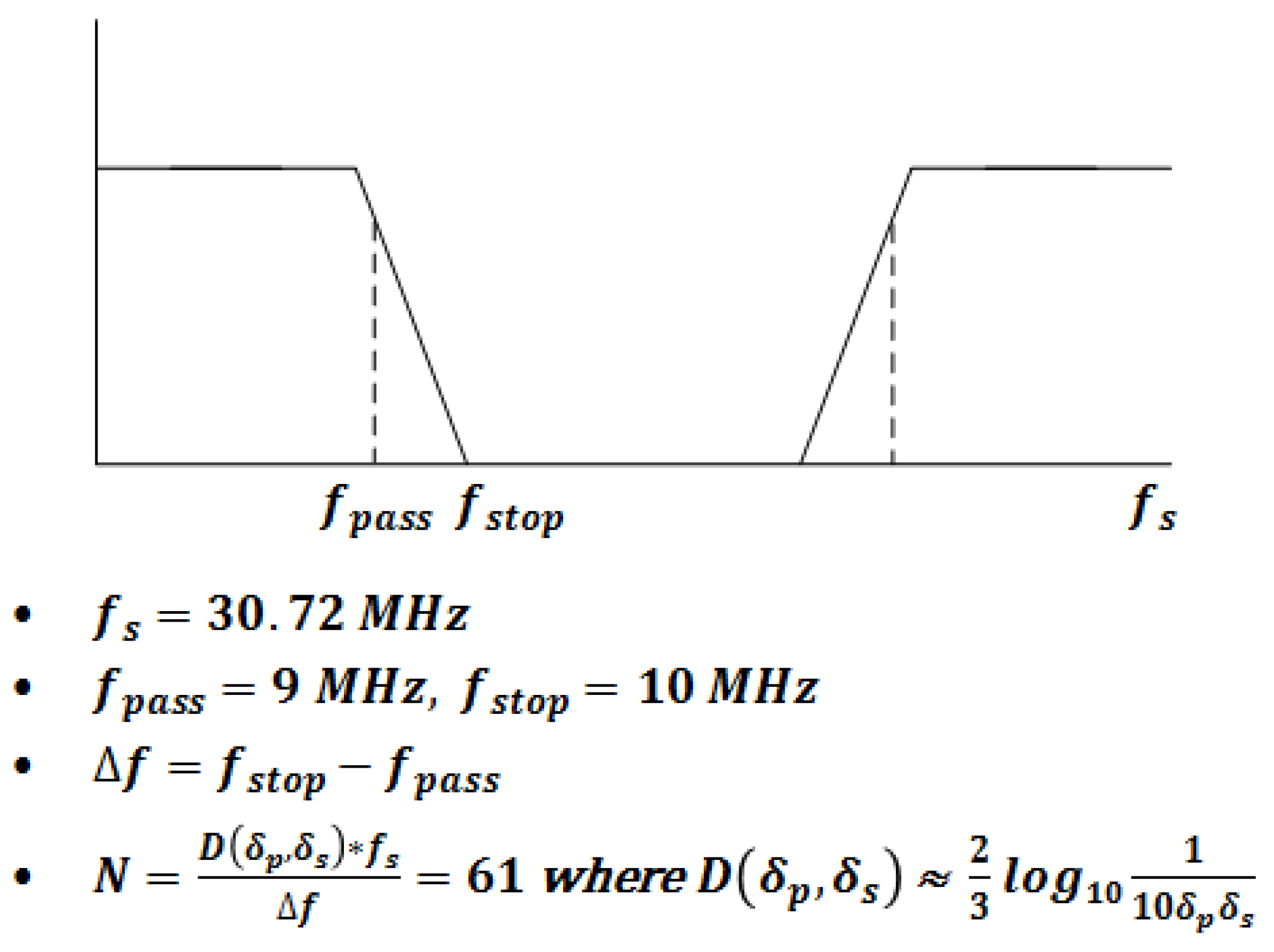
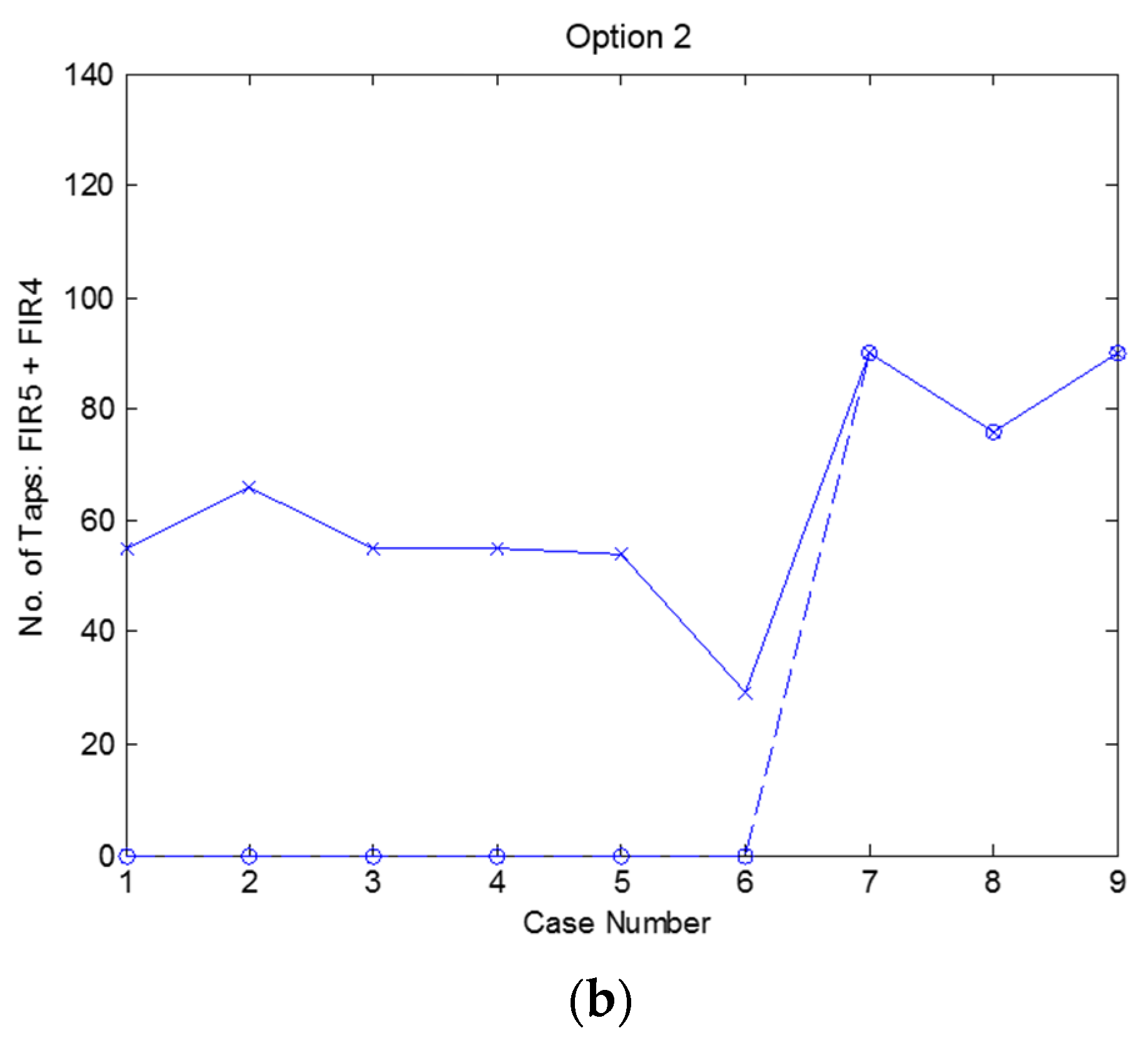
3.5. FIR5 (Channel Selection Filter)

FIR5 (channel selection filter or CSF) at the final stage rejects adjacent channel interference including the inband blocker and the narrowband blocker, which can be much stronger than the desired signal. This imposes the highest performance on FIR5, which does not conduct decimation. The left half of Figure 14 shows the input of FIR5 (CSF) and the right half shows the output of FIR5 in case of LTE (20 MHz + 20 MHz). At the input of FIR5, carrier 1 was located around the origin (center frequency) and carrier 2 was in the middle of the graph together with the inband blocker that was more than 20–30 dB larger, than carrier 1. After passing through FIR5 (a low-pass filter), the inband blocker became similar or smaller than carrier 1 and also carrier 2 became considerably smaller by over 40 dB. The inband blocker lost its adverse influence after it passed through the fast Fourier transform (FFT) processor in the OFDM receiver.
The filter coefficients were obtained over all the 10 cases or frequency modes and for carrier 1 and carrier 2. The coefficients for both carrier 1 and carrier 2 show symmetry and the numbers of coefficients were 31, 30, 31, 32, 27, and 29 and 32, 43, 32, a d32 for cases 1–6 and 10–13, respectively, concerning carrier 1, and the number of coefficients are 32, 32, 32, and 32 for cases 10–13, respectively, as to carrier 2.

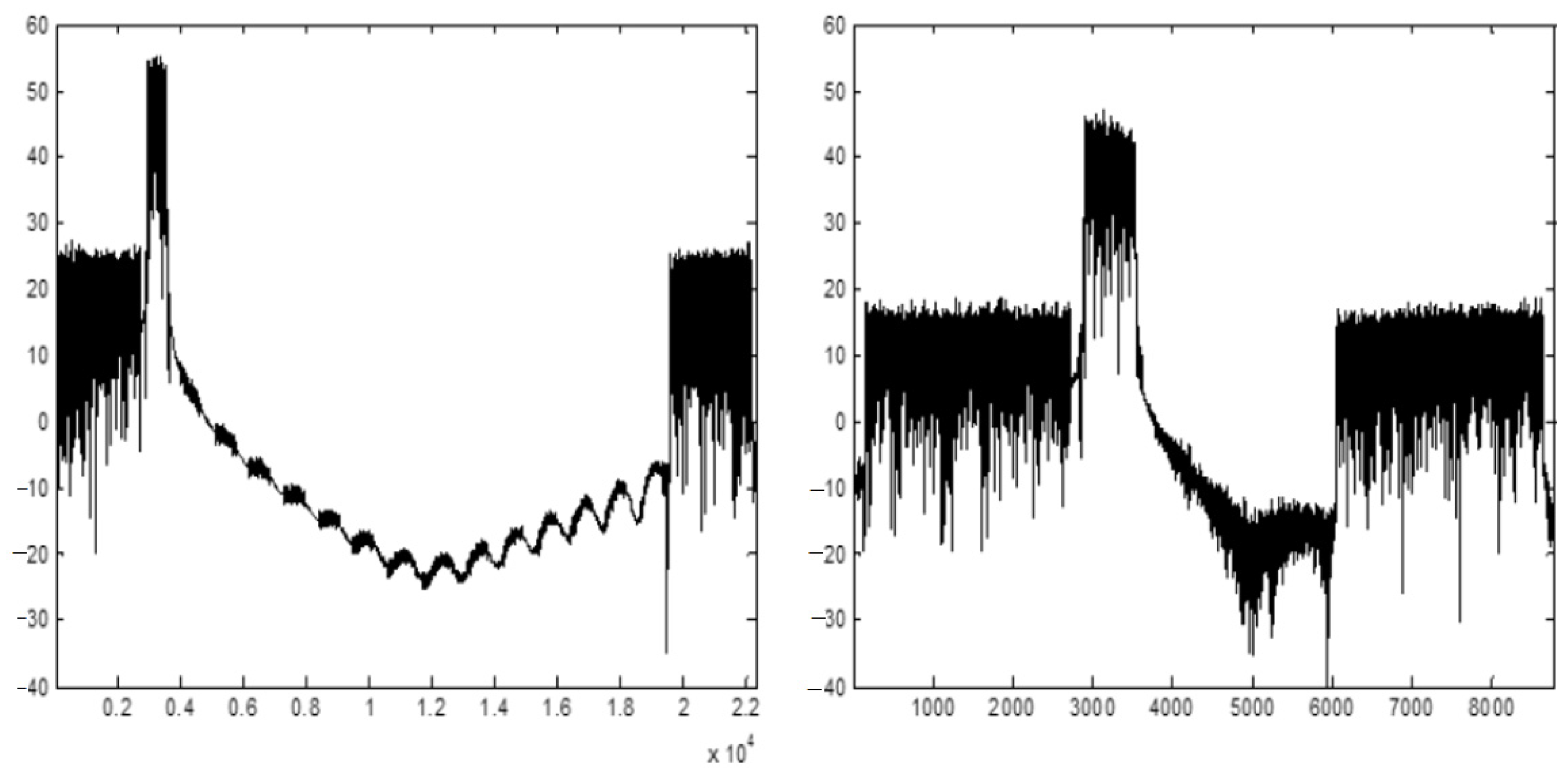
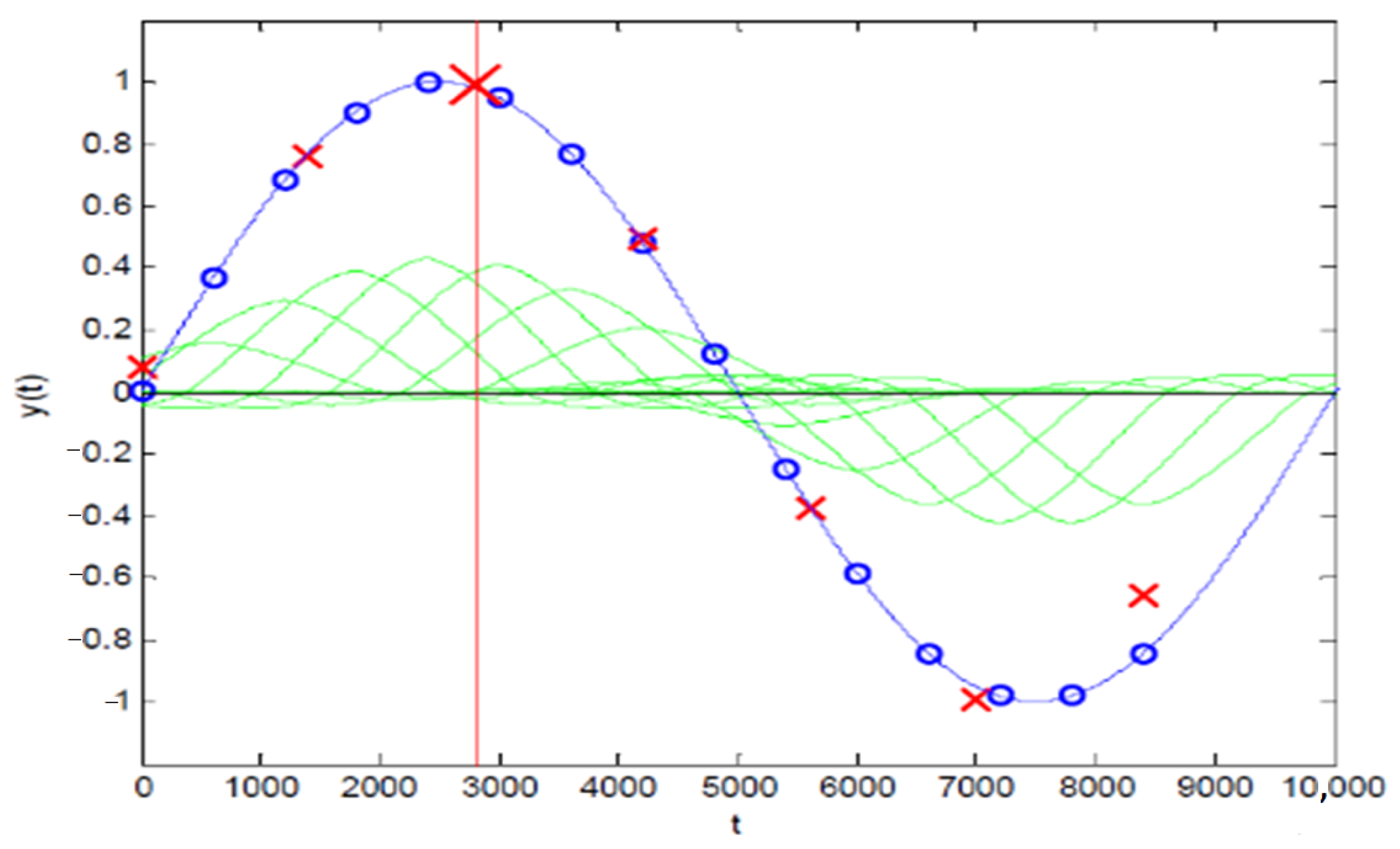
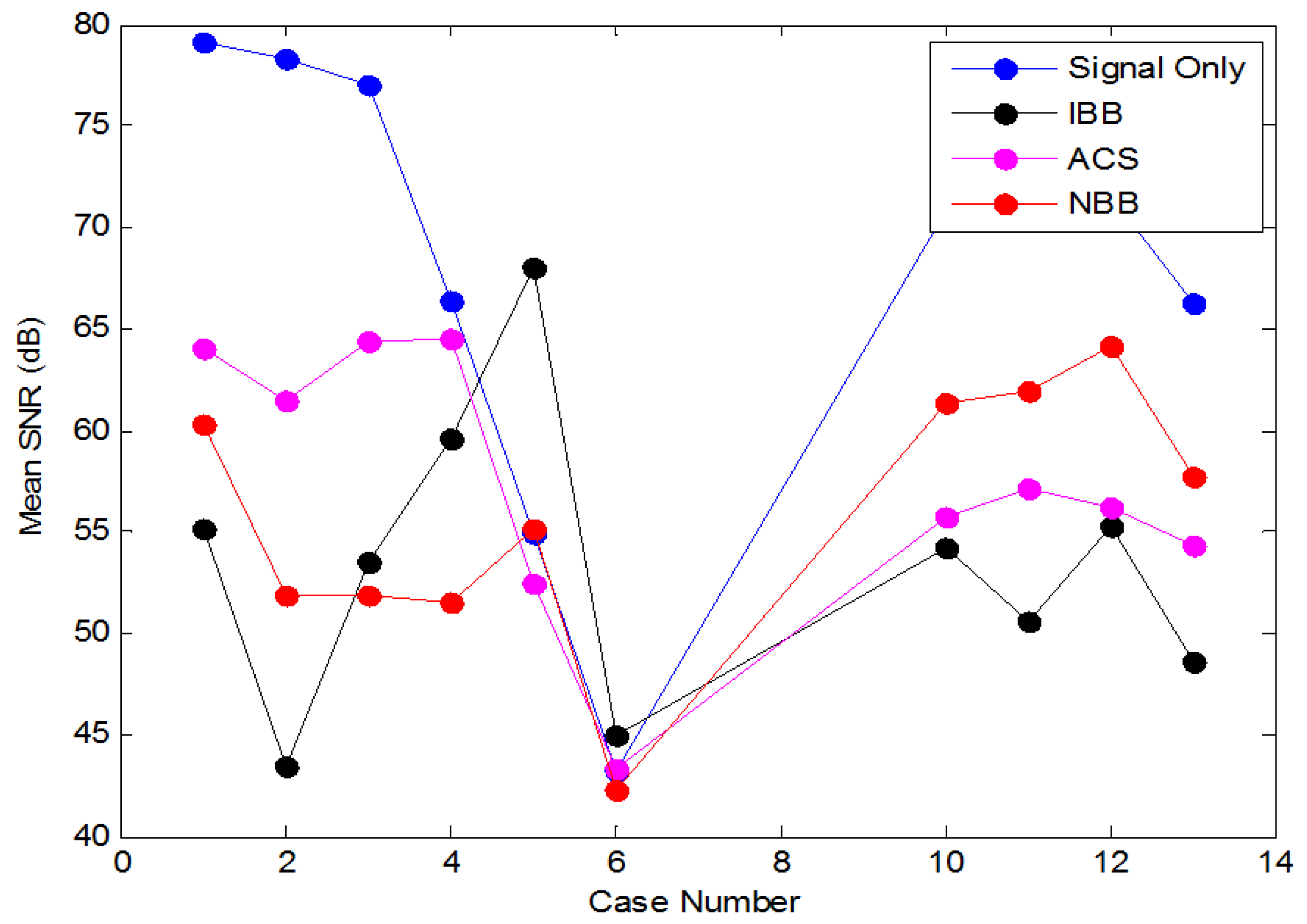
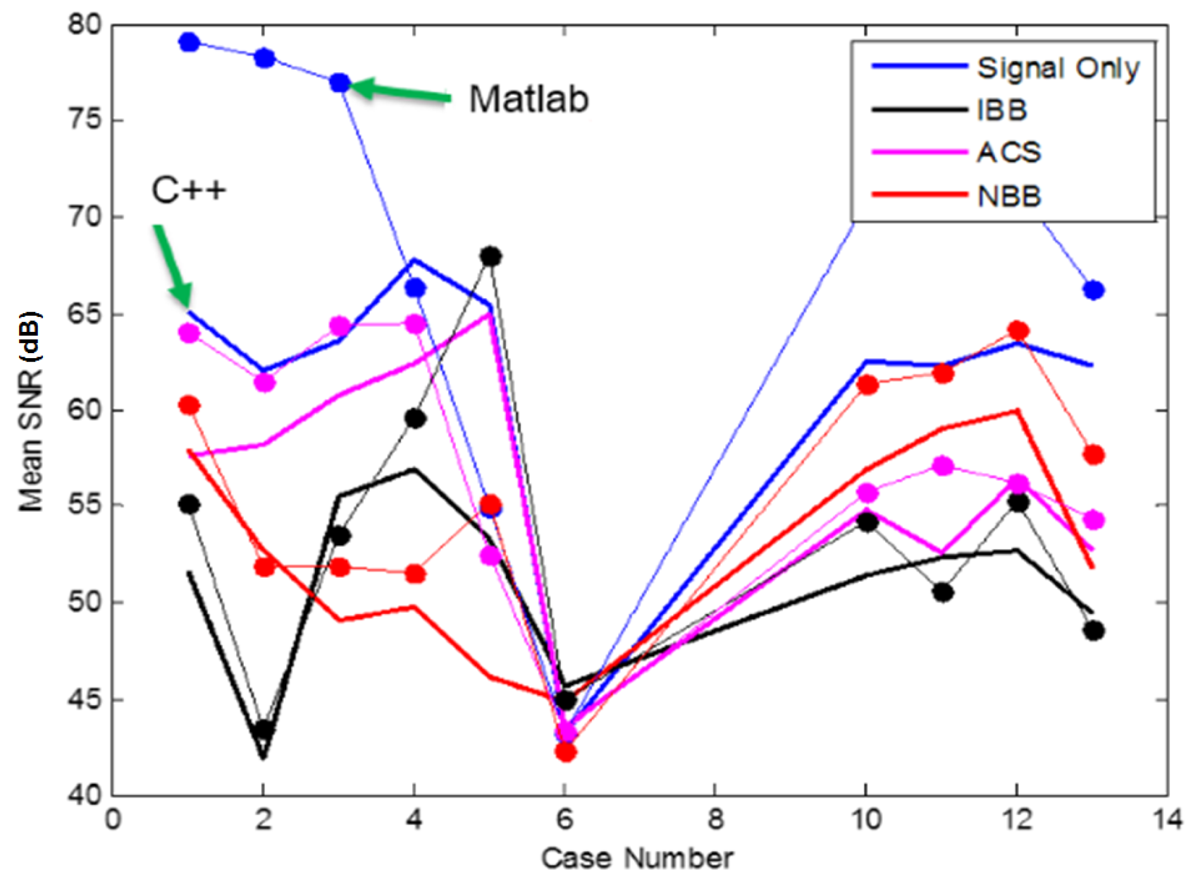
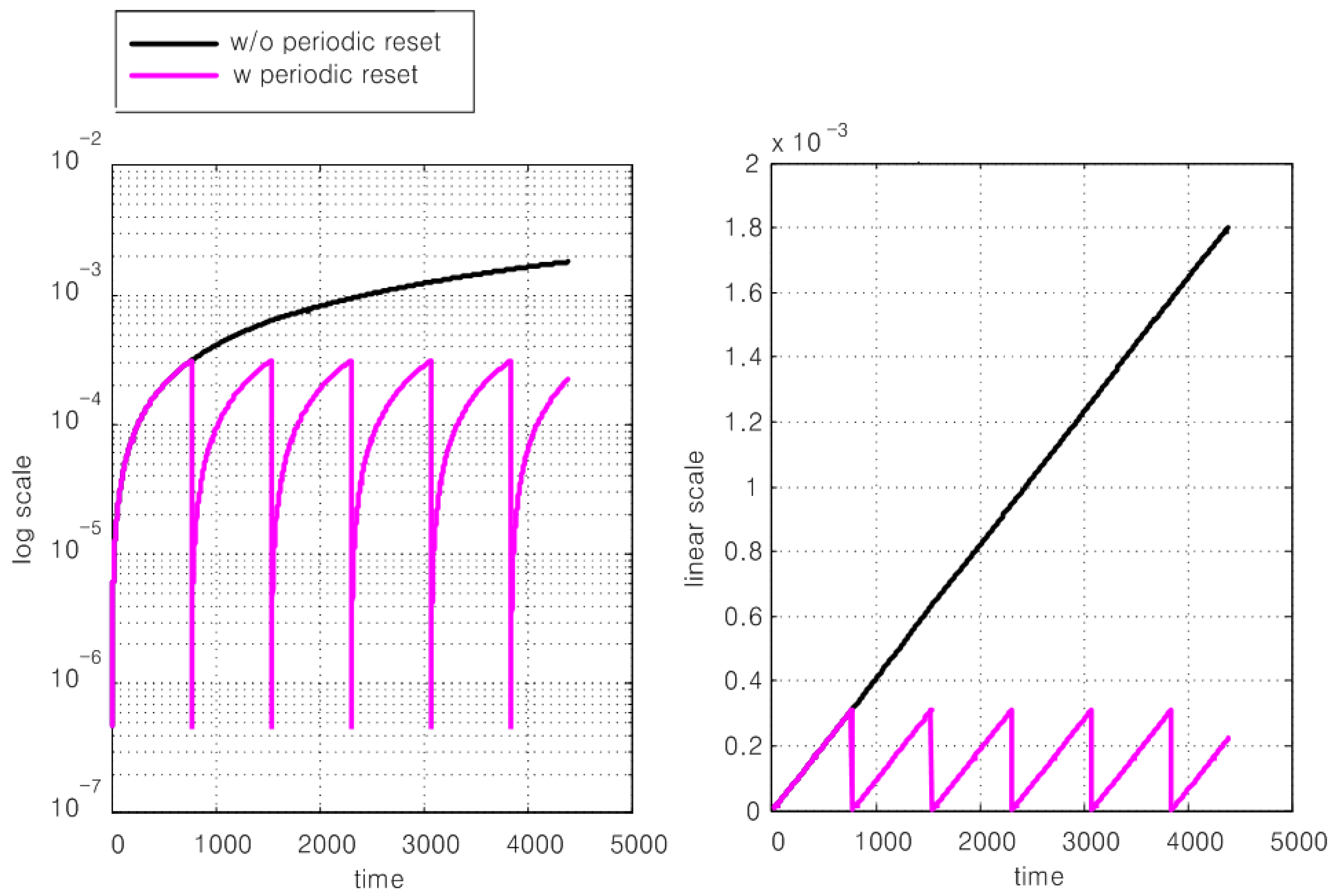
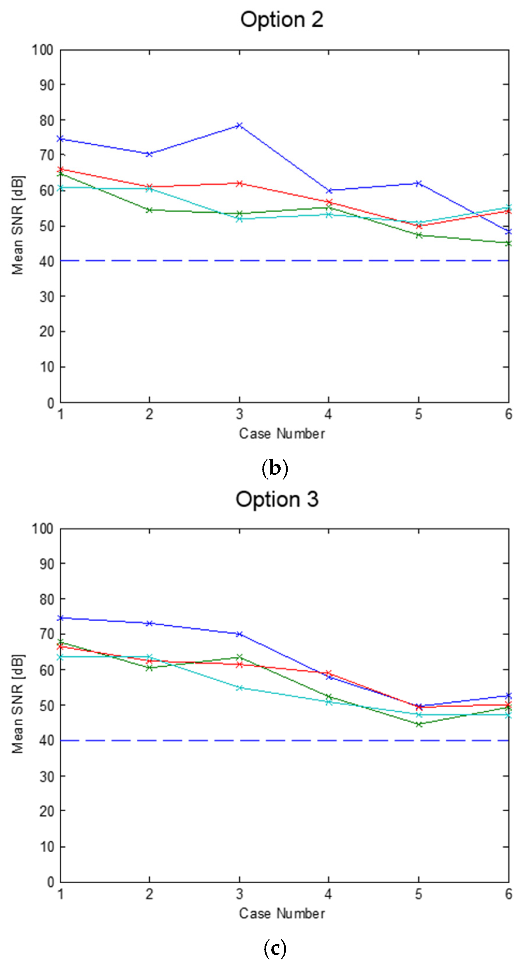
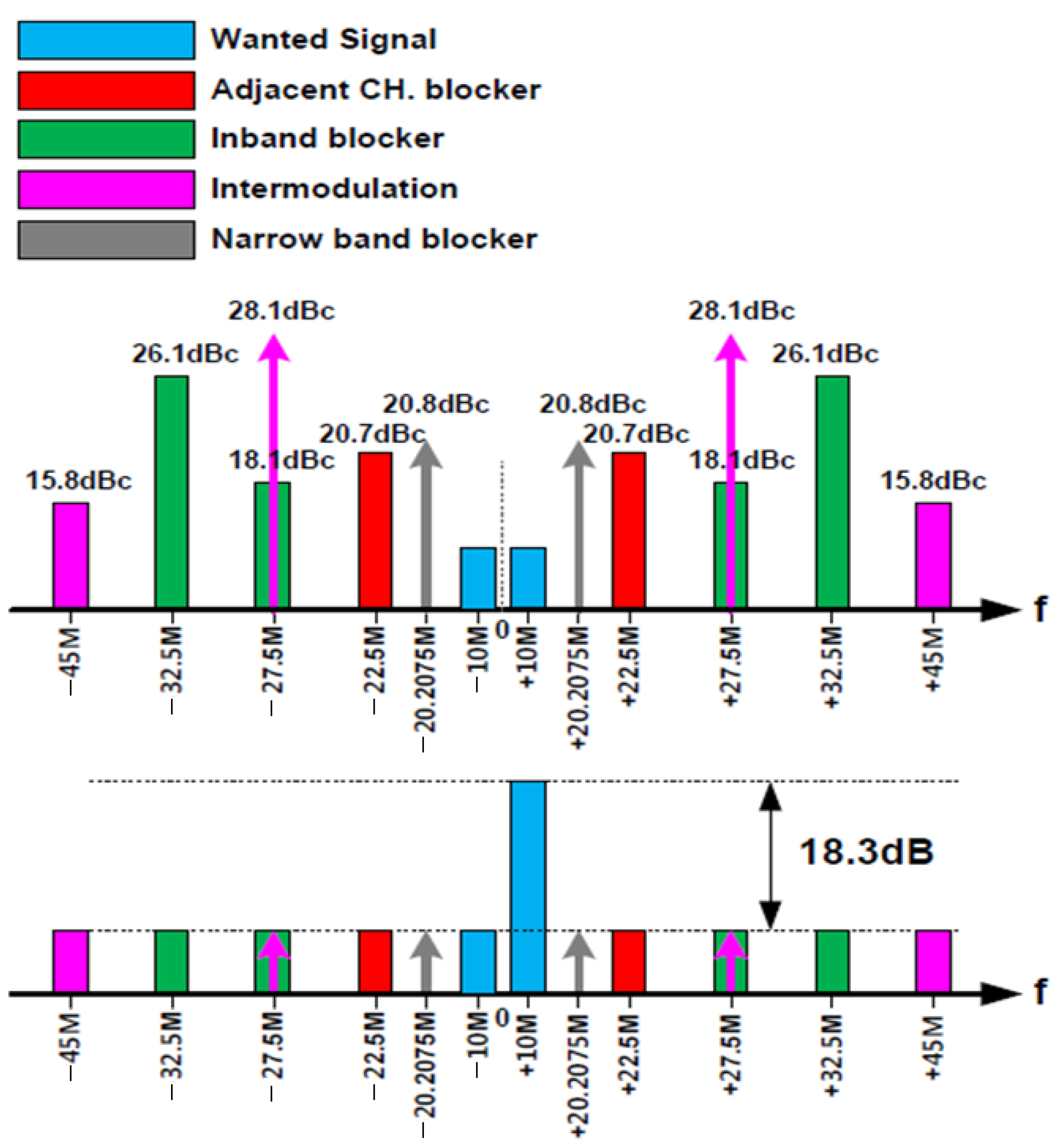
4. Simulated Results of the Overall DFE Architecture

The frequency-domain signals at the outputs of individual building blocks are sketched in Figure 15. Adjacent channel selectivity (ACS) and 20 MHz + 20 MHz LTE CA were assumed. Signal (a) is the output of the ADC, where the blue line is for the signal and the red line is for the interference in ACS. Signal (b) is the output of the CIC filter or FIR1, which operates on the signal (a). Signal (b), which is decimated and filtered, is shown in Figure 15 in the spectral domain as well. Signal (c) is the output of FSRC, which is fed with signal (b). FSRC can filter the desired signal more sharply than the CIC filter or FIR1, which is plotted in Figure 15 [23]. Signal (c) that is the FSRC output is fed to the DM, which translates or relocates the carrier instead of suppressing interference. As is plotted, the carrier frequency of signal (d) is shifted in the minus direction (leftward) relative to that of signal (c). Signal (e) is the output of CAF1 where further suppression occurs with respect to signal (d) and the last-step decimation is conducted. Up to this point, however, the interference amplitude is as yet larger than the desired signal amplitude. The last building block, CSF1, of the receiver DFE attenuates the interference substantially, for signal (f).
The DFE filter requirements are derived from various 4G LTE-A specifications. For instance, in case of LTE contiguous CA with an aggregate bandwidth of 40 MHz and for a 3rd-order Butterworth-type analog lowpass filter with a 3 dB frequency of 20 MHz, prior to the ADC, the specification at the analog filter output is shown in the middle of Figure 16 and the specification at the DFE filter output is shown at the bottom of Figure 16. As shown at the top of Figure 16, wanted signals, adjacent channel blockers, inband blockers, intermodulation components, and narrowband blockers are all taken into account for the proposed DFE that is compliant with LTE-A. From Figure 16, the DFE filter requirements were readily derived. Namely, the DFE filter with a center frequency of 10 MHz and a 3 dB bandwidth of 20 MHz, the attenuations at 20.2075 MHz, 22.5 MHz, 27.5 MHz, 32.5 MHz, and 45 MHz were to be 39.1 dB, 39.0 dB, 46.4 dB, 44.4 dB, and 34.2 dB, respectively.
The mean SNR was used as a performance measure, which was the SNR obtained at the 1-tap equalizer output in the terminal modem receiver. The output of the implemented DFE was fed to the Matlab-modeled OFDM receiver and the error between the receiver output and the original transmitted information was translated into the SNR on average. The performance of the proposed DFE was evaluated at the output of the OFDM receiver, which helped to capture the system impact of each design decision of the DFE. The OFDM receiver mainly consisted of cyclic prefix removal, FFT, and single-tap equalization. The synchronization and the channel estimation were assumed to be ideal. Our simulation results show that the frequency distortion introduced by the DFE (e.g., drooping) can be successfully removed by the standard OFDM receiver.
Figure 17 displays the mean SNR for the desired signal only (blue), the SNR in the case of the inband blocker (IBB) coexists (black), the SNR in the case of the ACS with adjacent channel interference was assumed (pink), and the SNR in the case of the narrowband blocker (NBB) coexists (red). All the mean SNR values were obtained from simulation of the proposed DFE. The case numbers on the x axis, 1, 2, 3, 4, 5, 6, 10, 11, 12, and 13 represent ten frequency modes, 20 MHz, 15 MHz, 10 MHz, 5 MHz, 3 MHz, 1.4 MHz, 20 MHz + 20 MHz (CA), 20 MHz + 15 MHz (CA), 20 MHz + 10 MHz (CA), and 5 MHz + 5 MHz (CA), respectively. Simulated results with IBB, ACS, and NBB were all exhibited to demonstrate that the proposed DFE was 3GPP-compliant. Relative to the signal only scenario, IBB, ACS, and NBB scenarios would lead to 11–36 dB degradation but all the mean SNR values were still above 40 dB. To summarize, the mean SNR values met the 40 dB specification of LTE-A for all the ten cases or frequency modes with our proposed and implemented DFE.
After taking the hardware behavior into account, the C++ cycle-accurate model is developed from the Matlab and C++ functional models. Figure 18 shows how a bit-accurate model was derived from the cycle-accurate model by using a class fixedDT. x(6,2) denotes the number of bits above the decimal point is 6 and the number of bits below the decimal point is 2. In order to evaluate cycle-accurate and bit-accurate performances, each hardware block was modeled both cycle accurately and bit accurately. The cycle-accurate model updates all the registers every cycle so that the content of each register varied in a cycle-accurate manner, as exemplified in the left part of Figure 18. Moreover, in order to facilitate the bitwidth optimization, a new C++ class called fixedDT was introduced. Once a fixedDT class was instantiated with the number of integer bits and the number of fractional bits, it took into account all the fixed-point effects such as quantization and overflow, by making use of the C++ operator overloading. This helped to make the relevant bitwidth optimization more efficient.
Figure 19 shows the mean SNR values for the Matlab model (small circles connected by solid lines) and the C++ bit-accurate model (solid lines). Blue, black, pink, and red represent signal only, IBB, ACS, and NBB coexisting, respectively. The bit-accurate model attained a slightly less mean SNR than the Matlab model but still met the 40 dB required specification of the LTE-A standard. The ten cases in the x axis corresponded to the ten frequency modes. The discrepancy between the C++ model and the Matlab model lay in the range of 0.5–15 dB and was the largest in the signal only scenario but all the scenarios (signal only, IBB, ACS, and NBB) met the 40 dB mean SNR requirement (which corresponded to an error vector magnitude or EVM value well below 1%, assuming 64 QAM or quadrature amplitude modulation).

5. Hardware Implementation and Experimental Results

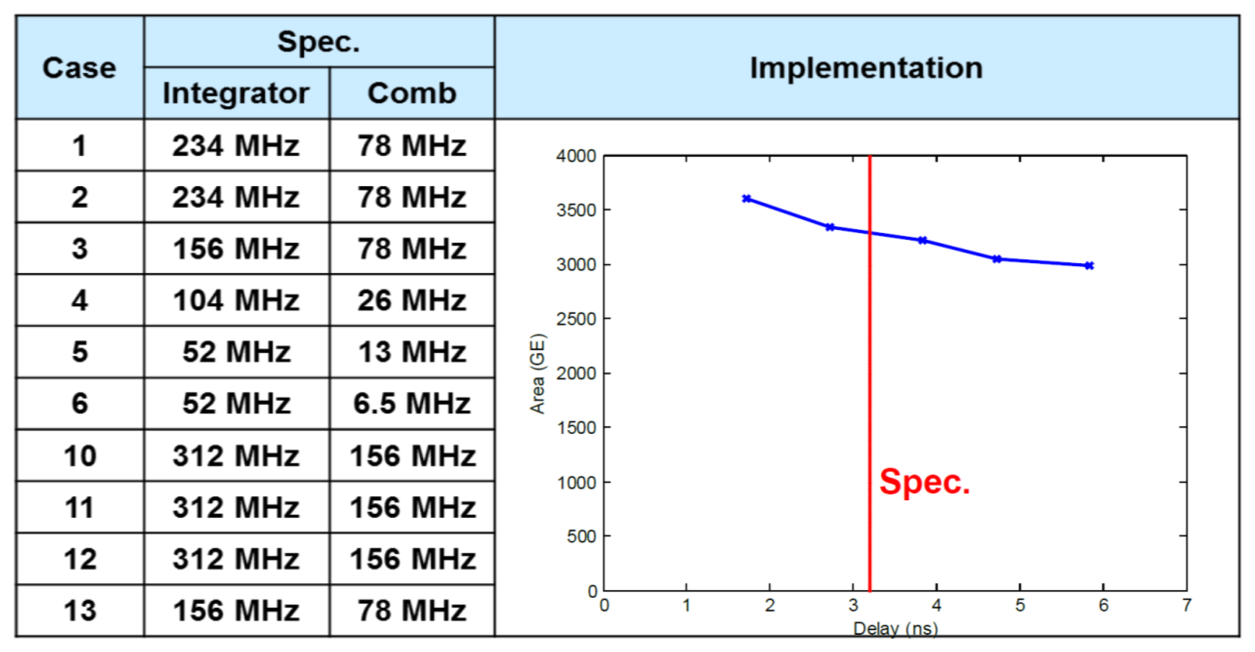
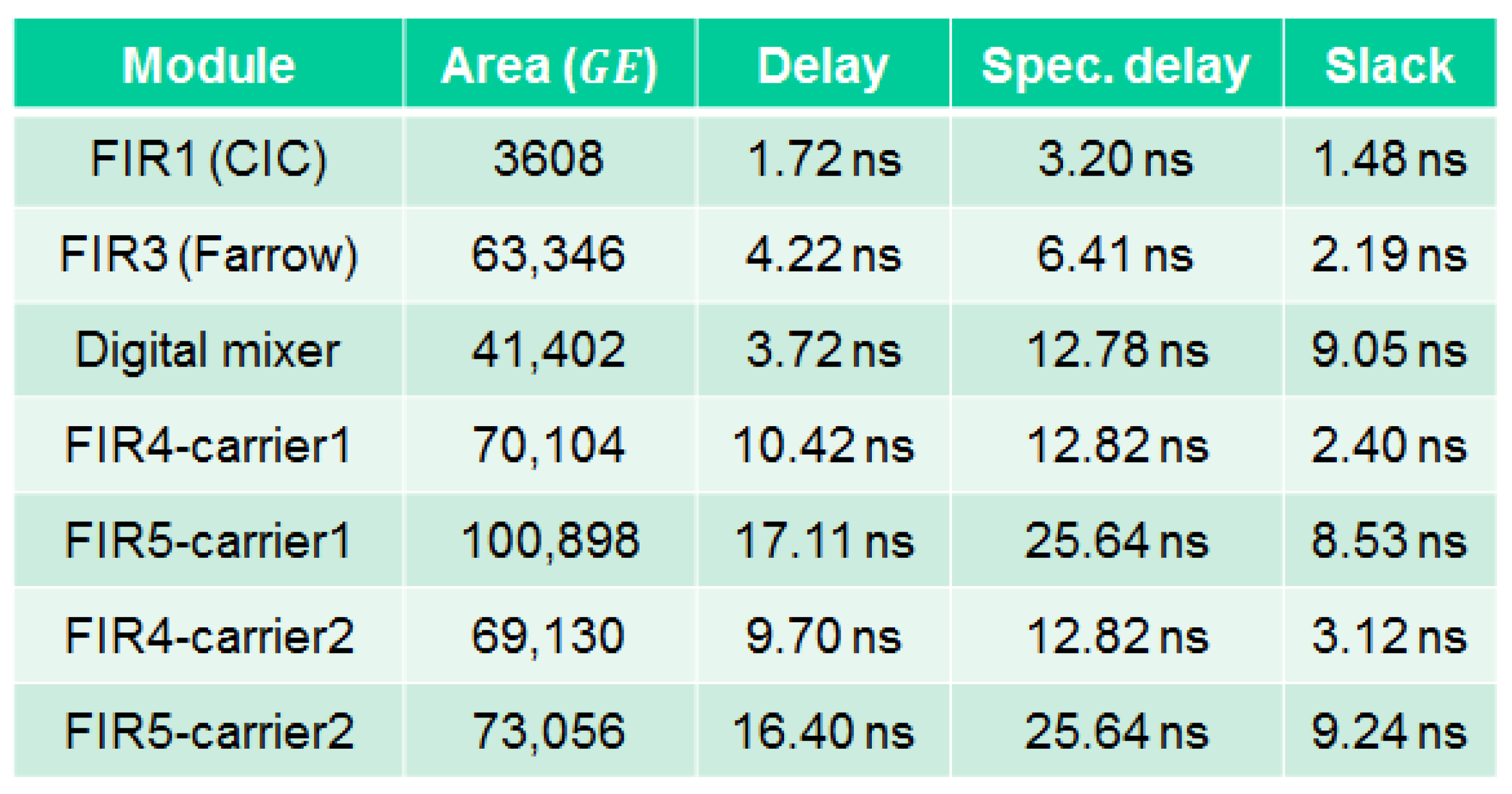
5.1. FIR1 (CIC Filter)

Word lengths of the integrator in the CIC filter were implemented as in Figure 20a, which shows the structure of the integrator. The output of the ADC, out_ADC, was set to vary such that −2 ≤ out_ADC < +2 since the output may not be expressed with only one integer bit for some interference scenarios. After the signal from the ADC passed through the flip-flop (FF), the signal was sign-extended to 14 bits in the integer part (instead of the original 2 bits at out_ADC), since the maximum value of the sum of the impulse responses over all the cases was turned out to be 4096 or 212, as shown in Figure 20b. By means of this internal 12-bit word length increment (rather than using a scaling factor by 1/4096 prior to FIR1), overflow was obviated.
The comb filter was designed and implemented, whose structure and word lengths are displayed in Figure 21a. As with the integrator, it only consists of the addition operations. At the last stage of it, a right-shift-by-x operation was used to return the bitwidth above the decimal point back to 2 as in the input of the CIC filter. The right-shift values x were 7, 7, 4, 8, 8, 12, 4, 4, 4, and 4 for cases 1, 2, 3, 4, 5, 6, 10, 11, 12, and 13, respectively, according to the sum of the impulse responses. The decimator can be simply implemented by using a counter. The decimation factor of each case is listed in Figure 21b.
The output of FIR1 was set to quantize 16 bits in total, instead of 26 bits, in consideration of the speed of FIR3 (Farrow interpolator). In summary, the CIC filter including scaling dispenses with any internal multiplication operation and the quantization error is output only once at the end. Critical path delays are different for different implementation methods, namely, the ASIC synthesis and the FPGA placement and routing (P&R). The critical path delay for the ASIC synthesis in a 180 nm CMOS technology was 1.72 ns that consisted of the 0.66 ns delay from the (26-bit + 26-bit) adder and the remaining path delay, highlighted in red in Figure 20a, whereas the critical path delay for the FPGA P&R was 2.42 ns that consisted of the 1.674 ns adder delay and the remaining path delay, highlighted in green in Figure 20a. The critical paths seem different with ASIC and FPGA but as the procedure is the same in each stage, they may be regarded as being identical. The reason that the ASIC is faster than the FPGA is attributed to the ASIC synthesis targeting speed at the cost of area while the FPGA P&R could not attain the same goal. The ASIC synthesis results are summarized in Figure 22, where the required delay of 3.205 ns or 1/312 MHz is denoted in red. Area was expressed in 2-input NAND gate equivalent (GE) gate count. The actual delay was placed to the left of the red line and hence the CIC filter operated in compliance with the specification.

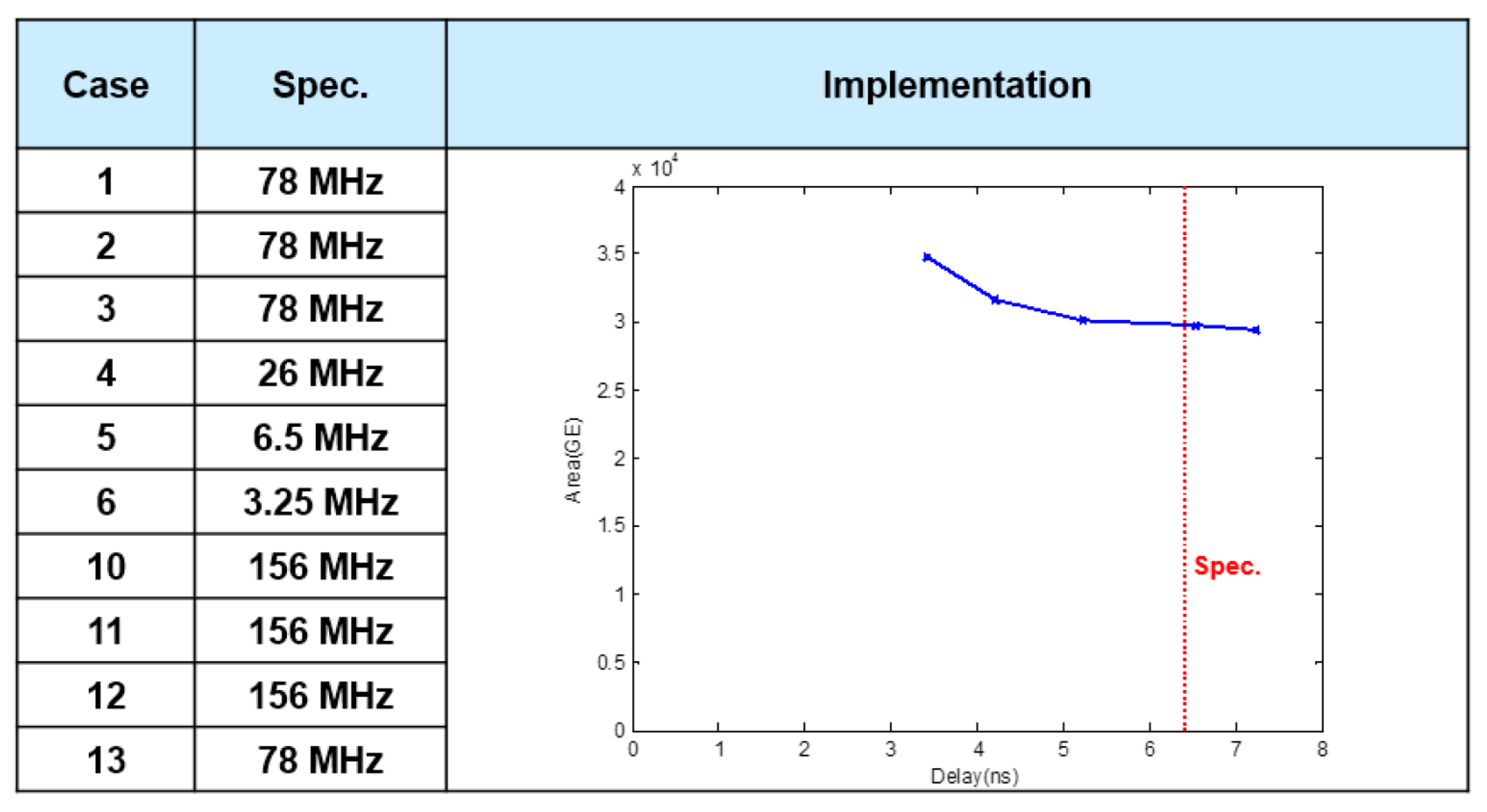
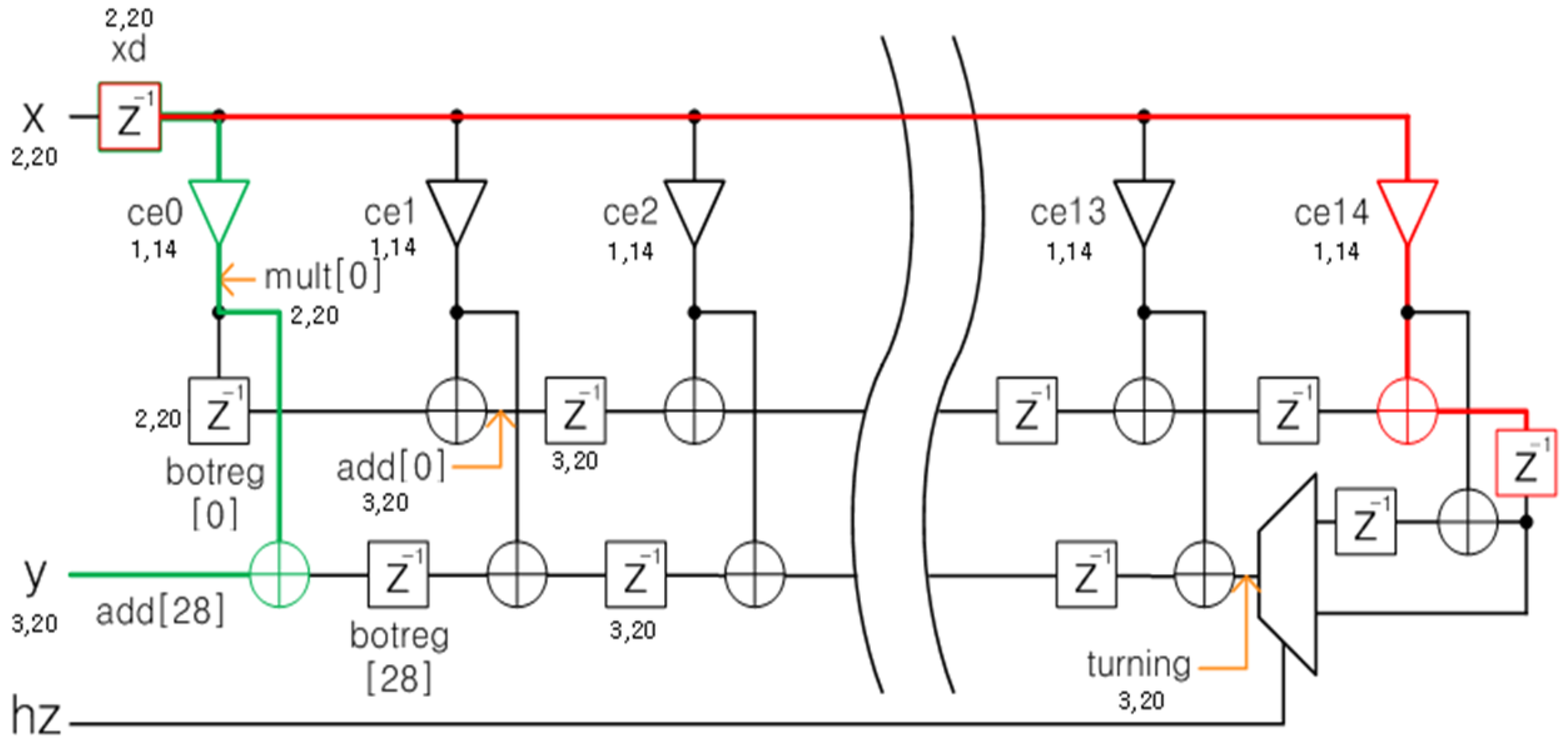
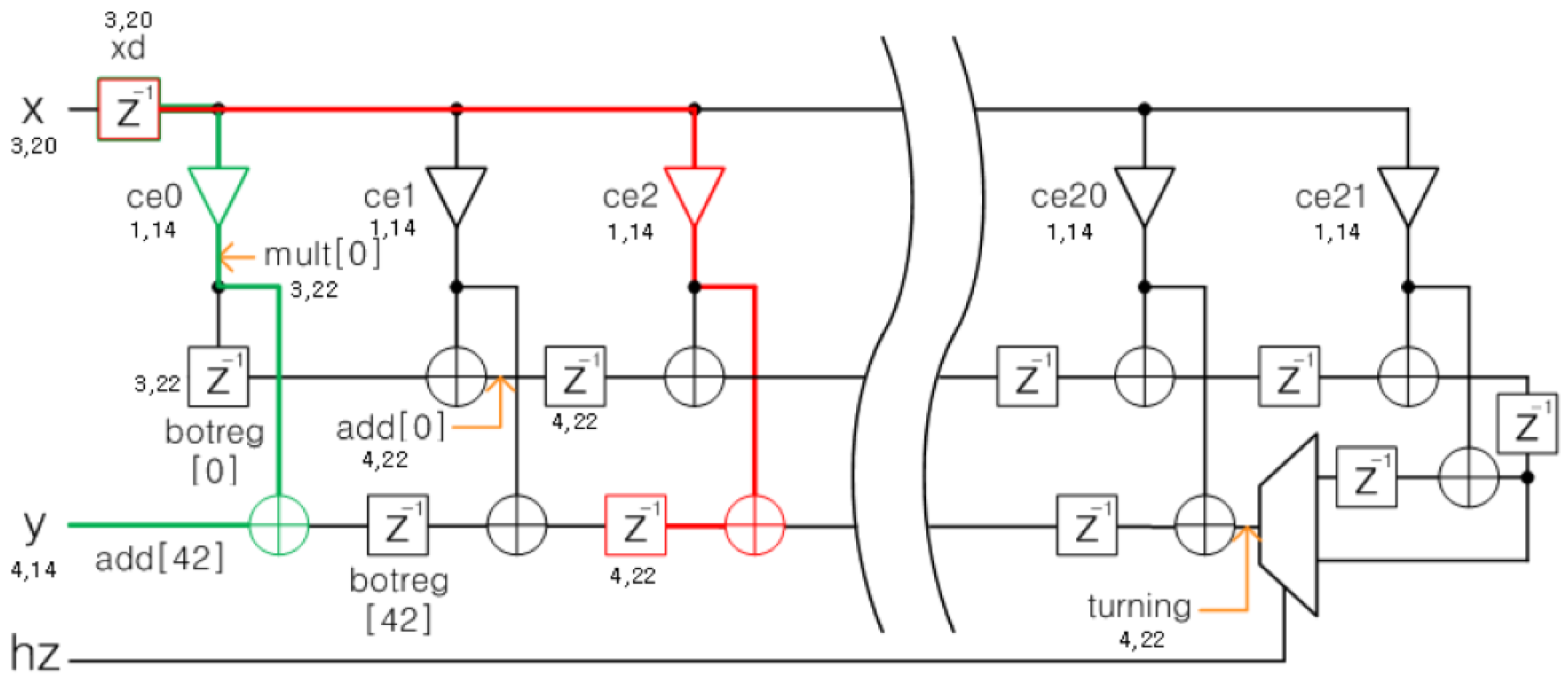
5.2. FIR3 (Farrow Interpolator)
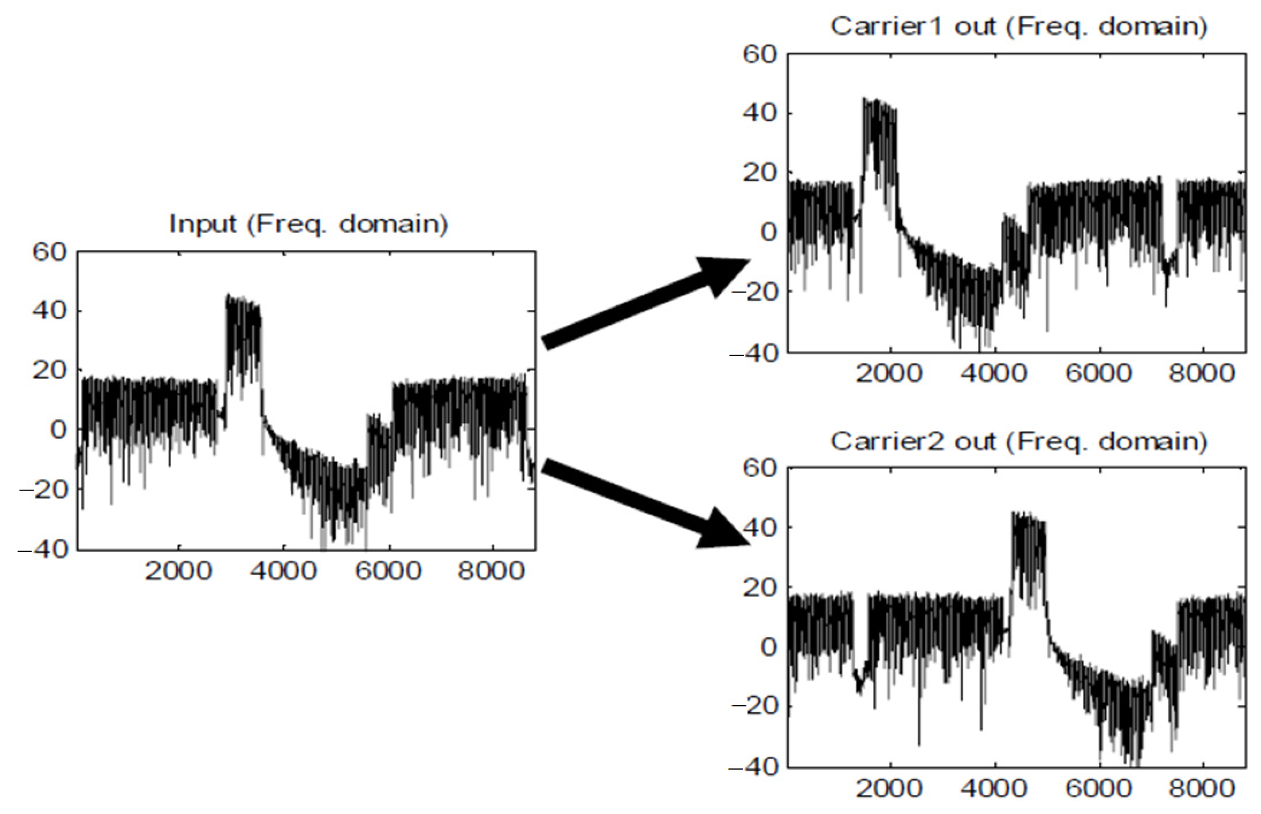
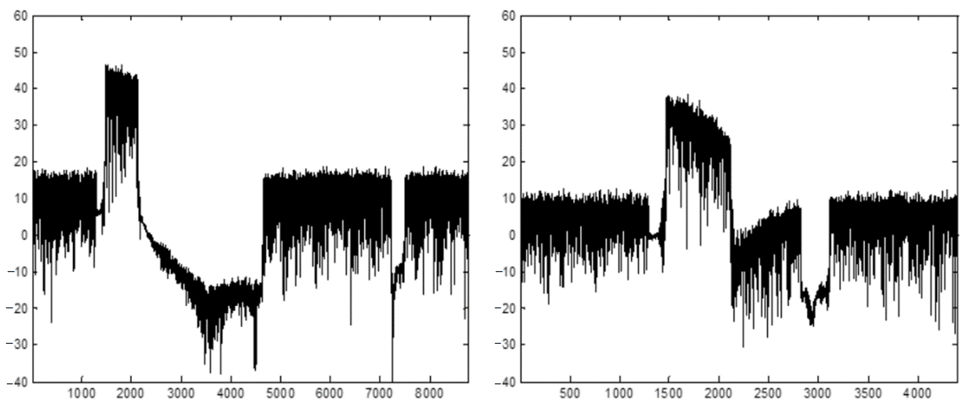
Figure 23 exhibits the block diagram of cubic-Lagrange-polynomial-based FIR3 (Farrow interpolator) in the LTE DFE, where mu signifies μkTo, To_inv means 1/To, and xd indicates the input signal. The 1-bit signal, condition, became 1 when mu exceeded ToTi and became 0 otherwise.
The upper part of FIR3 consists of the subpart for obtaining μk by means of multiplying μkTo by 1/To and the subpart for obtaining μk, μk2, and μk3 in sequence by repeatedly multiplying μk. Thus, the upper circuitry represents the 0-th-, first-, second-, and third-order terms from left to right. Below the part exists the integrate-and-dump circuitry, which serves the purpose that the input signal was accumulated to obtain the output signal and subsequently the accumulated signal was delivered to the lower part of FIR3, according to the condition signal. The lower part of FIR3 was made up of polynomial coefficients with respect to μk. The length of the interpolation filter was 6To, which means the polynomial operations were run over 6 intervals, and hence a total of 6 cubic polynomials of μk existed, leading to a total coefficient count of 24. This was also identified in the farrow_matrix inside the Matlab script inset. At the very end of the circuitry existed a multiplier, which multiplied the signal by a scale value for coefficient normalization. The scale value for the polynomial coefficients was supplied externally since it varied according to To and Ti. In the case of the functional model, this value was 0.969467455621302 for Ti/To = 128/325 and 1.454201183431953 for Ti/To = 192/325. In the case of the bit-accurate and the RTL models, it was 0.969451904296875 for Ti/To = 128/325 and 1.454193115234375 for Ti/To = 192/325. It was calculated from Ti/To/832 where 832 was the total sum of the internal polynomial coefficients. By multiplying the normalization value at the end separately (instead of normalizing the internal coefficients), the internal coefficients could be constantly used regardless of the Ti/To value.
The proposed integrate-and-dump circuitry was governed by the 1-bit signal, condition, as highlighted in cyan in Figure 23. By means of the operation of the integrate-and-dump circuitry, the period of the output of FIR3 was an integer multiple of the clock period, although the output of FIR3 held a non-integer value resulting from a rational-number interpolation. For instance, in the case of a fractional interpolation by 128/325, the period of the FIR3 output was twice or three times the input period and in the case of a fractional interpolation by 192/325, the period of the FIR3 output was equal to or twice the input period.
The critical path of FIR3 in the ASIC is highlighted in red in Figure 23, in which case the critical path had a 19-bit-by-25-bit multiplier between two flip-flops since this was the widest multiplier in the circuitry. The former flip-flop had a delay of 0.52 ns and the multiplier had a delay of 3.72 ns, a total of 4.22 ns critical path delay. The critical path of FIR3 in the FPGA (Xilinx XC6VLX550T) is highlighted in green in Figure 23. Whereas polynomial coefficient multiplication was carried out with high-speed constant multipliers in the case of the ASIC synthesis, digital signal processor (DSP) slices with general multipliers were utilized even for constant multiplication in the case of the FPGA P&R. The critical path for the FPGA was composed of a 16-bit constant × 27-bit signal multiplier and also two 27-bit adders in series between two flip-flops, where the first flip-flop incurred a 0.283 ns delay, the multiplier gave rise to a 3.236 ns delay, and the adders reflected a delay of 1.245 ns + 0.996 ns, along with a delay of 2.298 ns from the remaining path, totaling a 8.06 ns critical path delay.
Figure 24 shows synthesis results and required operating frequencies of FIR3. Each required operating frequency was determined by the input frequency of each case and the decimation factor of FIR1 (CIC filter) that is the prior stage. For instance, the input frequency of case 10 (20 MHz + 20 MHz LTE CA) was 312 MHz and FIR1 conducted decimation by 2, and hence FIR3 for case 10 should run at 156 MHz to say the least, which is the most stringent requirement. The graph in Figure 24 exhibits the 6.41 ns or 1/156 MHz clock period in the red line. It is shown that as the required speed increased, a small amount of area (GE) increased. The ASIC synthesis in 180 nm CMOS technology was carried out so as to obtain a critical path delay less than 6.41 ns. In view of the P&R routing delay of the ASIC, a delay margin of 2 ns was secured and a 4.22 ns-delay Farrow interpolator was designed and synthesized, corresponding to 236.97 MHz in frequency.

5.3. Digital Mixer

A digital mixer was proposed based on an LUT and periodic reset. It consists of the local oscillator [24] and the complex multiplier. The local oscillator had a structure shown in Figure 25. The real_in and imag_in signals were received from the LUT since different angles should be supported for different cases. For cases 10, 11, 12, and 13, the angles were (mixer 1, mixer 2) = (58.5938, 58.5938), (43.9453, 58.5938), (29.2969, 58.5938), and (29.2969, 29.2969), respectively, in units of (degrees, degrees).
The proposed digital mixer can get rid of the phase error accumulation by adopting a counter, cnt, and multiplexers, as shown in Figure 25. More specifically, the local oscillator has a feedback structure to produce cumulated I and Q signals for a given angle each clock cycle. Owing to this, the oscillator was susceptible to phase error accumulation from quantization. In this design, the angle that the oscillator supports was found and the digital mixer was periodically reset by a counter (cnt in Figure 25) in order to prevent phase error accumulation. Figure 26 exhibited the phase errors without a counter (black) and with a counter for periodic reset (pink), from which it is shown that the proposed digital mixer could effectively prevent phase error accumulation.
Next, the complex multiplier for the digital mixer was designed and implemented such that the output from FIR3 (Farrow interpolator) was multiplied by the local oscillator output. Its structure is displayed in Figure 27. The complex multiplier received FIR3_realout and FIR3_imagout from FIR3 and also received real_ff2 and imag_ff2 from the local oscillator to execute the operation.
After the ASIC synthesis, the digital mixer composed of the local oscillator and the complex multiplier had a critical path delay of 3.72 ns consisting of a 1.1 ns delay of the (22-bit × 21-bit) multiplier plus a 1 ns delay of the 42-bit adder plus a remaining path delay. After the FPGA P&R, the critical path delay, consisting of a 3.519 ns delay of the (22-bit × 21-bit) multiplier plus a 0.619 ns delay of the 42-bit subtractor plus a remaining path delay, was 5.602 ns in total. The critical paths for ASIC and FPGA are highlighted in red and green, respectively, in Figure 27. As is evident, it is confirmed that the critical paths for ASIC and FPGA indicate the same path in effect since both paths had the same-sized multiplier and adder/subtractor.
The ASIC synthesis results of the digital mixer in a 180 nm CMOS technology were summed up in Figure 28, where the required delay of 12.82 ns or 1/78 MHz was denoted as a red line. The digital mixer was synthesized to reveal a delay value that lies to the left of the red line at the expense of a small area overhead.

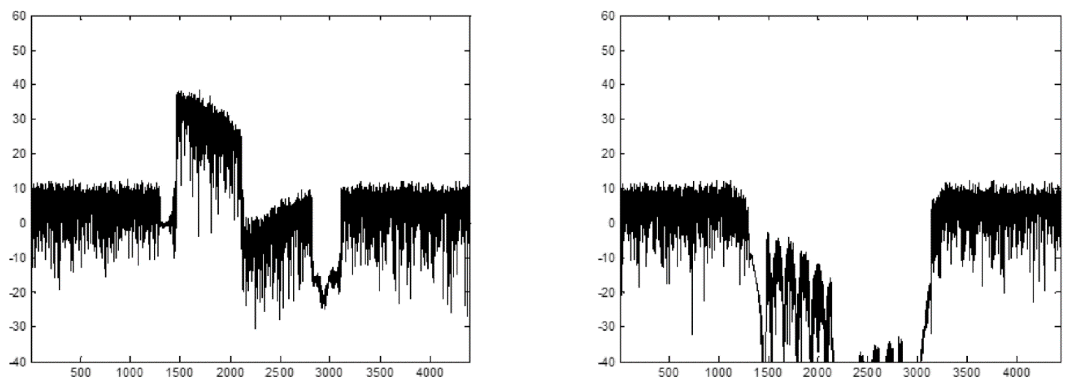
5.4. FIR4 (Carrier Aggregation Filter)

The block diagram of FIR4 (CA filter) in LTE DFE is sketched in Figure 29. The FIR4 low-pass filter was in the transposed form of the FIR filter and designed in view of coefficient symmetry. Among the coefficient sets with respect to the LTE DFE operating modes, the set with the largest number of coefficients was of size 30 and hence the number of distinct coefficients in the FIR filter hardware was 15. The upper part of Figure 29 multiplies the input signal by the coefficients, yielding x⋅ce0, x⋅ce1, x⋅ce2,…, x⋅ce14, 15 signals in total, which were connected to two paths in the opposite order, taking symmetry into account. The lower part of Figure 29 took on the ordinary transposed FIR filter form. What differs from the typical structure is the multiplexer (MUX) on the right part, which determines whether the center coefficient value is applied once or twice to the input signal, depending on the select signal of the MUX. If the select signal is 0, the center coefficient is subject to symmetry as are other coefficients. If the select signal is 1, the center coefficient is only applied once. The output period of FIR4 is the input period of FIR4 multiplied by the decimation factor.
The critical path with the ASIC in a 180 nm CMOS technology is highlighted in red in Figure 29. There were a 15-bit × 22-bit signed multiplier and a 23-bit adder between two flip-flops and this kind of form was identical to all the 15 coefficients, and hence the path with the largest delay reflecting the physical wire delay as well will be the path for coefficient 14 (ce14). In the case of the FIR4-carrier 1, the flip-flop + multiplier + adder overall delay was 0.29 ns + 5.36 ns + 4.77 ns = 10.42 ns and similarly in the case of the FIR4-carrier 2, the overall delay was 0.32 ns + 4.99 ns + 4.39 ns = 9.70 ns. The critical path with the XC6VLX550T FPGA is highlighted in green in Figure 29. It also consists of a multiplier and an adder. In the case of the FIR4-carrier 1, the critical path delay was the multiplier + adder + route delay, equaling 3.441 ns + 0.890 ns + 1.375 ns = 5.706 ns while in the case of the FIR4-carrier 2, the delay was 3.441 ns + 0.712 ns + 1.699 ns = 5.852 ns.
FIR4 has a module for carrier 1 and another module for carrier 2 in order to support LTE CA. Similarly to the ASIC synthesis of FIR1, FIR3, and the digital mixer, FIR4 is also successfully synthesized to meet the LTE requirements. The required operating frequency is the same as the FIR3 (Farrow interpolator) output sampling frequency. In the case of the 128/325 interpolation, the FIR3 output period was twice or three times its input period and in the case of the 192/325 interpolation, the FIR3 output period was identical to or twice its input period. Therefore, the harder to meet for the FIR3 output was twice its input period in the case of 128/325 whereas the harder to meet in the case of 192/325 was x1 its input period. For instance, in case 10 (LTE CA 20 MHz + 20 MHz), FIR3 had an input period of 1/156 MHz and ran the 128/325 interpolation, and hence FIR4 should operate with a frequency of at least 78 MHz. This is because FIR4 should operate with twice the FIR3 input period, which equaled 2/156 MHz or 1/78 MHz. FIR4-carrier 1 should meet the required critical path delay of 1/78 MHz = 12.82 ns. Giving a 2 ns or so delay margin, the synthesis results exhibited a critical path delay of 10.42 ns, meeting the requirement at the cost of a small amount of area increase. Similarly for FIR4-carrier 2, the required critical path delay was 12.82 ns, and giving a 2 ns margin, the ASIC synthesis resulted in a 9.70 ns critical path delay, also satisfying the requirement.

5.5. FIR5 (Channel Selection Filter)

FIR5 (CSF) has the same structure and operating principle as FIR4 in the preceding subsection and the only differences were that FIR5 had more filter coefficients and did not handle decimation. The largest number of coefficients was 43 (for case 11) among the ten LTE DFE frequency modes and if implemented in hardware, 22 in view of symmetry.
The critical path in the ASIC (180 nm CMOS) is highlighted in red in Figure 30, which includes a (15-bit × 23-bit) signed multiplier and a 26-bit adder. In the case of FIR5-carrier 1, the critical path delay was the delay of (the first flip-flop + multiplier + adder) delay, which amounted to 17.11 ns while in case of FIR5-carrier 2, the critical path delay was 16.40 ns. The critical path in the XC6VLX550T FPGA after the P&R is highlighted in green in Figure 30. Identical with FIR4, FIR5 in the FPGA also had a multiplier and an adder in the critical path, as with FIR5 in the ASIC. With FIR5-carrier 1, the overall critical path delay was the (multiplier + adder + route) delay, which equaled 3.441 ns + 0.961 ns + 1.792 ns = 6.194 ns while with FIR5-carrier 2, the overall critical path delay equaled 3.441 ns + 0.796 ns + 1.464 ns = 5.701 ns.
As with the preceding building blocks, FIR5 was synthesized in a 180 nm CMOS ASIC and its required operating frequencies, which are the inverse of the FIR4 output period, were readily obtained as 39 MHz, 39 MHz, 19.5 MHz, 13 MHz, 3.25 MHz, and 3.25 MHz and 39 MHz, 39 MHz, 39 MHz, and 19.5 MHz with respect to cases 1–6 and 10–13, respectively. The FIR4 output period equaled its input period multiplied by its decimation factor and hence the required frequency of FIR5 was equal to the required frequency of FIR4 divided by the decimation factor of FIR4. As with FIR4, FIR5 in LTE DFE also had individual modules for carrier 1 and carrier 2 to support CA. The demanded critical path delay of FIR5 (CSF) with carrier 1 was 1/39 MHz or 25.64 ns, which was much looser than the critical path delay obtained in practice with a margin of 2 ns, which was 17.11 ns, and thus no speed constraint was necessary during the synthesis. The demanded critical path delay of FIR5 with carrier 2 was also 25.64 ns and without any speed optimization the FIR5 filter was synthesized with the critical path delay of 16.40 ns that was much shorter than the demanded one.
The CSF lay at the back of the decimation chain and hence the speed requirement was relaxed while the hardware complexity was high. By contrast, the CIC filter lay at the head of the chain and hence the speed requirement was most stringent while the hardware complexity was low (since the CIC filter dispensed with any multiplier).

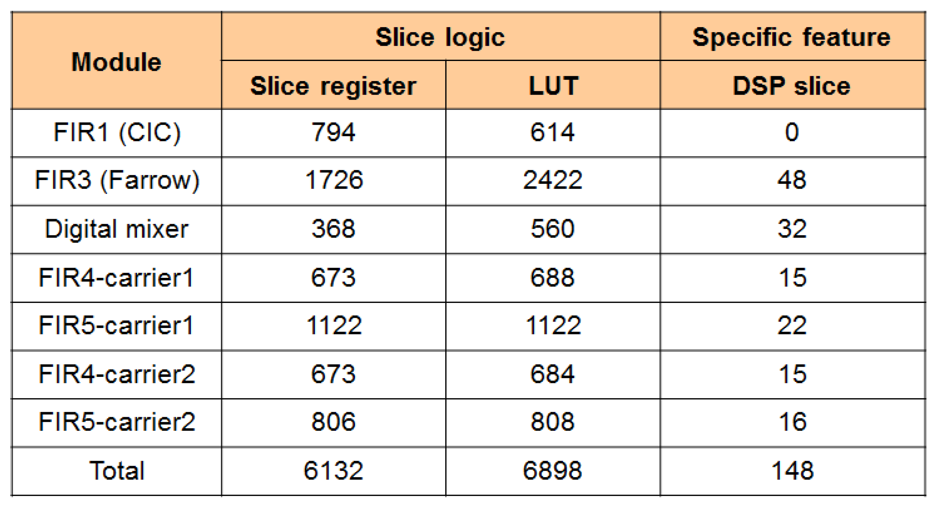
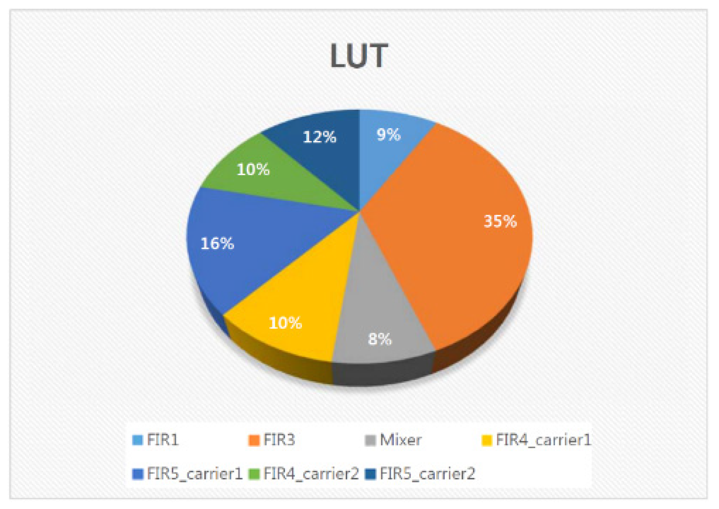
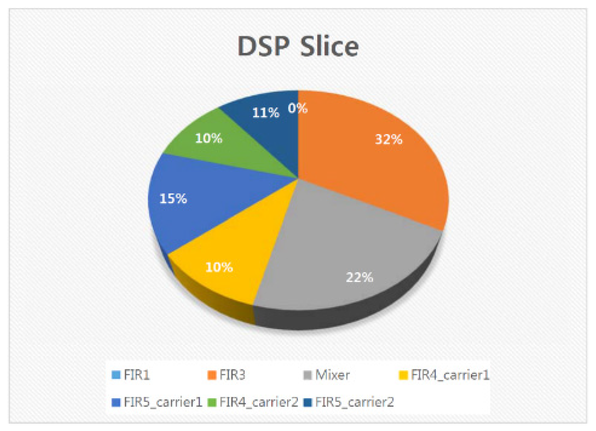
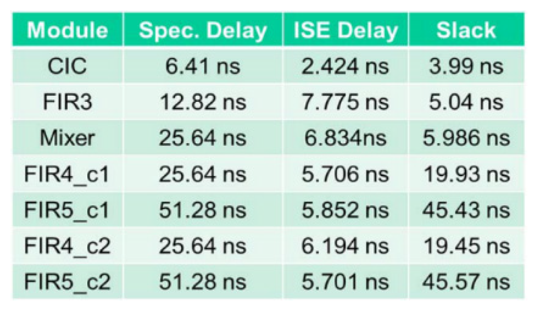
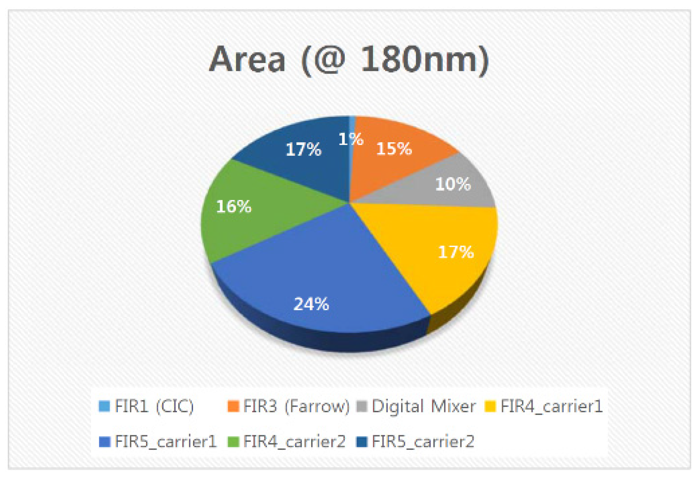
5.6. ASIC Synthesis of the Overall DFE Architecture

Since the building blocks of the proposed DFE operate at different rates, the blocks were synthesized individually in a 180 nm digital CMOS technology. Areas (2-input NAND GE), delays, and slacks (= specification delay − delay) of the DFE building blocks are summarized in Figure 31. The most stringent delay was taken as the specification delay. FIR5_carrier1 had the largest size with the slowest speed, owing to many coefficients and accordingly many multipliers that were programmable multipliers to support a multitude of cases, which also degraded speed relative to constant multipliers. A slack of >2 ns was considered during design but FIR1 had a slack of 1.48 ns. This block ran fastest of all at front of the decimation chain and hence a large margin was not easy to attain for it. FIR1 (CIC) had the smallest slack or timing margin while FIR5 had the largest slack secured. The pie graph for the areas of the building blocks is shown in Figure 32. FIR1 (CIC filter) occupied 1% of the entire area, FIR3 (Farrow interpolator) occupied the entire area by 15%, the digital mixer by 10%, FIR4_carrier1 by 17%, FIR4_carrier2 by 16%, FIR5_carrier1 by 24%, and FIR5_carrier2 by 17%.

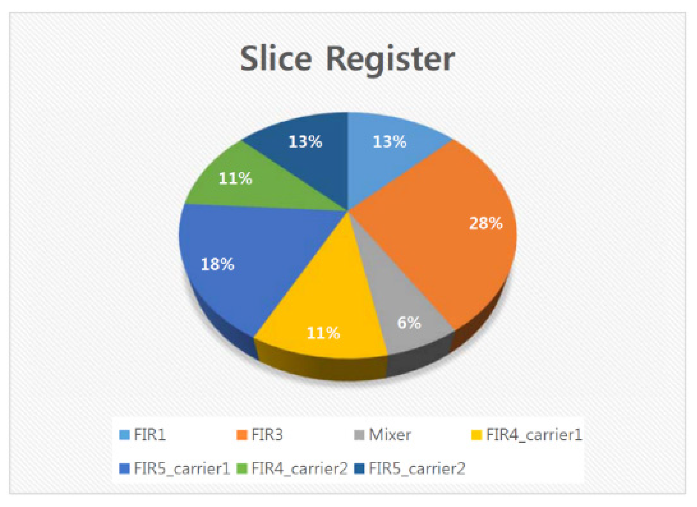
5.7. FPGA Placement and Routing Results of the Overall DFE Architecture
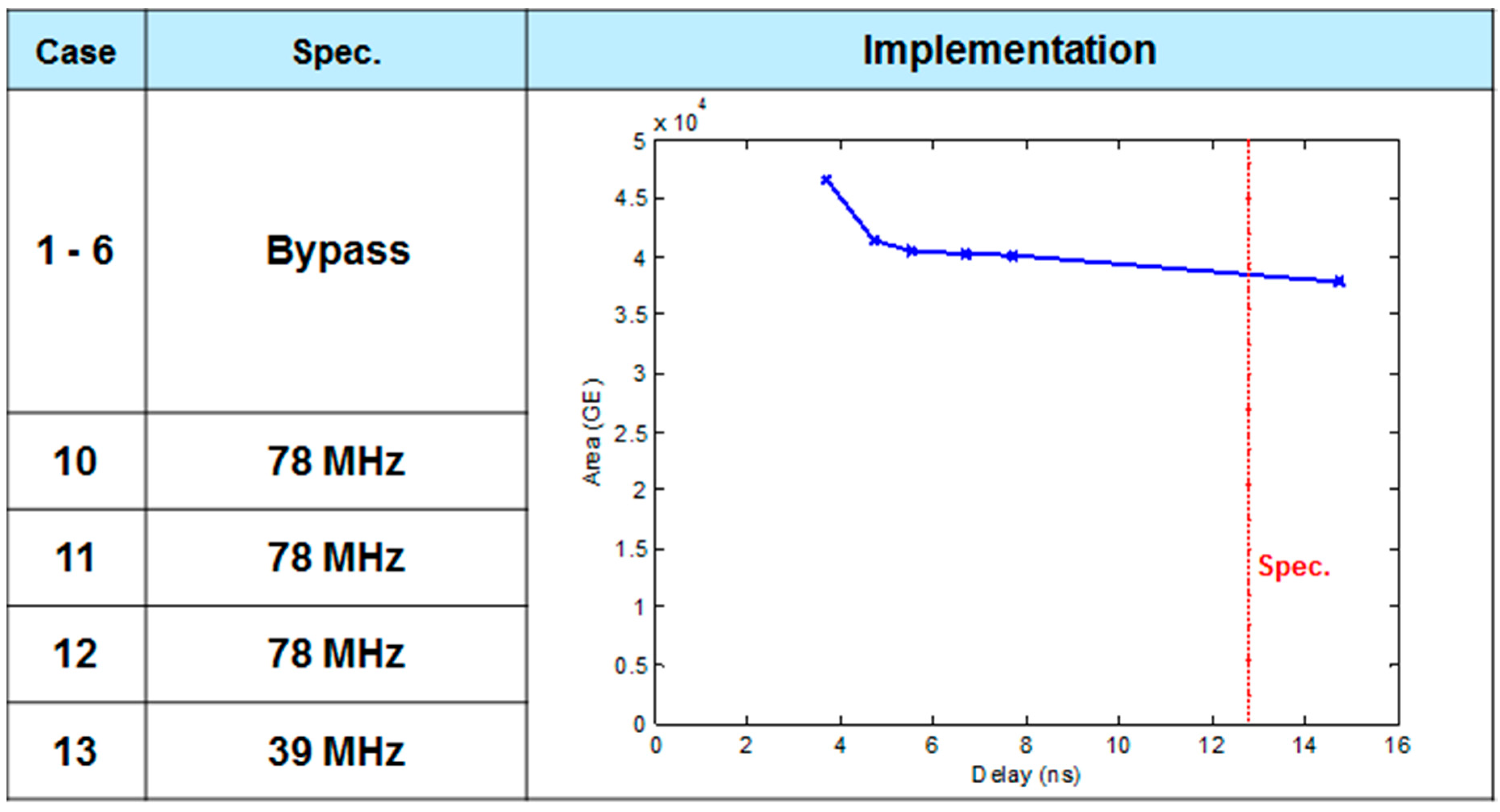
Different than the ASIC synthesis results, the FPGA (XC6VLX550T) P&R results show that FIR3 (Farrow interpolator), involving many multipliers, consumed resources most, which used the largest number of DSP slices. The resources used by the DFE building blocks are summarized in Figure 33. Since FIR1 (CIC filter) did not use any multiplier, it did not use any DSP slice. FIR3 (Farrow interpolator) used 24 coefficients for each of I and Q and hence 48 DSP slices were used. It also needs some conditions for carrying on operations, which increased complexity and also the count of LUTs and slice registers. The digital mixer also used many DSP slices. In the case of XC6VLX550T, each DSP slice could support a 25-bit × 18-bit multiplication. The digital mixer exceeded this bit range and needed an extra multiplier. Therefore, (1 + 1) × 8 = 16 DSP slices were needed and since there are two carriers, carrier 1 and carrier 2, 32 DSP slices were used in total. FIR4 and FIR5 use 14–22 DSP slices but since they need I and Q, 28–44 slices were used. Only 1% of the FPGA slice registers were used for all the building blocks in the DFE and only 2% of the LUTs were used while 24% of the DSP slices were used. Pie graphs for the use of slice registers, LUTs, and DSP slices are shown in Figure 34, Figure 35 and Figure 36, respectively.
After the FPGA implementation, speed performance was obtained, which reflects the routing effect as well. The P&R is carried out individually for each building block. An example (5 MHz + 5 MHz) CA case was tested and the P&R timing report is shown in Figure 37. ISE (integrated synthesis environment) delay is the delay obtained after the FPGA P&R. Sufficient timing margins or slacks are secured for the building blocks in the proposed LTE CA DFE.

5.8. Discussion

The overall design process of the proposed DFE is shown in Figure 38, composed of three stages, namely, calculation of the filter specification, calculation of the filter coefficients, and simulation of the DFE together with the OFDM receiver model. From the chosen decimation ratio of each filter, the filter specification was calculated, followed by the calculation of the FIR filter coefficients. Subsequently, with the calculated filter coefficients and the data bitwidths (set by the fixedDT class), the DFE together with the OFDM receiver model was simulated to draw the mean SNR performance (and the area, which is typically proportional to the no. of filter coefficients). If the SNR is not met or if more than enough margin is left for the filter specification, this process is repeated to explore the design space and to optimize the overall system through manual tweaking of the decimation ratio, the filter specification, and the bitwidths, in this order.
This design process was more specified with a simple example for each stage of the design process in Figure 38. The first stage of the design process in Figure 38 was the calculation of the filter specification. To explain the first stage, three design options are illustrated in Figure 39, differing in the respective decimation ratios across the CIC filter, the FSRC filter, and the FIR4 filter. The decimation ratio of each filter determines the sampling rate or frequency fs of the filter. On the other hand, various blocker and adjacent channel selectivity requirements (coming from the standard spec itself) determines fpass, fstop, Δf = fstopfpass, δs, and δp, where fpass is the passband frequency, fstop is the stopband frequency, Δf is the transition width, δs is the stopband attenuation or suppression, and δp is the passband ripple, respectively. Next, from the computed filter specification, the no. of filter coefficients was calculated in the way illustrated in Figure 40 [25]. If, for instance, fs equals 30.72 MHz, fpass equals 9 MHz, and fstop equals 10 MHz, then the no. of filter coefficients, N, is readily calculated from Figure 40. The filter coefficients themselves were obtained on the basis of Parks-McClellan optimal FIR filter algorithm [26]. Finally, corresponding to the third stage of the design process in Figure 38, the overall DFE with the OFDM receiver model was simulated after the filter coefficients of all the filters are obtained.
Figure 41 illustrates the mean SNR values of options 1, 2, and 3 in (a), (b), and (c), respectively. The design space of the overall DFE system was explored for, for example, the three design options or candidates. From the worst case standpoint, the mean SNR values of option 1, across the six cases or frequency modes, leave higher margins above the required SNR of 40 dB, when compared with those of options 2 and 3, and hence option 1 will be chosen in this case. Figure 42 illustrates the sum of the no. of filter taps of the FIR4 and FIR5 filters. Up to case number 6 (i.e., without CA), option 1 served better in terms of the area. If all the cases are considered (including cases 7, 8, and 9 with CA), option 2 is in practice tantamount to option 1. Similar to the aforementioned example design options 1, 2, and 3, various candidates in the architecture design space were evaluated before the final DFE architecture was proposed.
A multitude of literatures deal with the DFE, including [2,3,4,5,6,7,8,9,11,12,13,17,27,28,29,30], and many of them are based on the CIC filter, Farrow interpolator, and the FIR filter. However, most of them address only the simulated results and few of them explain the ASIC or FPGA implementation in detail. The proposed DFE architecture in this paper was implemented in FPGA and ASIC in a rigorous manner such that the critical path delays were analyzed and the requirements of ten frequency modes (or cases) for LTE-A CA were all met. The parameters of all the building blocks in the proposed DFE were chosen after an extensive 3GPP specification study. The spectral-domain view is also shown for each building block of the DFE. The FPGA implementation results and the ASIC synthesis results of the proposed DFE were also analyzed in terms of timing margin, speed, area, and resource usage. The proposed DFE was constructed from a systematic design methodology based on abstraction levels from Matlab and C++ functional models through C++ cycle-accurate and bit-accurate models to RTL models, while the ADC model and the OFDM receiver model were also taken into account to give an overall receiver performance in terms of the mean SNR. A special class (fixedDT) was developed to methodically convert the cycle-accurate model to the bit-accurate model, so that the RTL model performance was guaranteed to be in line with the functional model, providing a more robust design implementation. Not only the overall DFE architecture was proposed to be compliant with the LTE-A CA, but also its building blocks, especially Farrow interpolator and the digital mixer, were refined and proposed to serve their purposes relevantly. Namely, the integrate-and-dump circuitry of Farrow interpolator was refined via a condition signal to provide appropriate timing for the output. Moreover, a digital mixer with an LUT, aided by the periodic reset functionality, was proposed to overcome the problem of phase error accumulation, which was demonstrated experimentally.
Another point that distinguishes our approach from others was that the OFDM receiver output was taken as the reference output, not the ADC input or output, in order to optimize the overall receiver system. The distortion that appears at the ADC input or output might be cancelled while it passes through the OFDM 1-tap equalizer.
Prospective research of the proposed DFE will be directed toward incorporating more functions into the DFE architecture, such as DC offset cancellation, I/Q estimation and compensation, and antidrooping filtering, as a means to digitally correct radio frequency impairments. Additionally the DFE chain for the radio transmitter, consisting of an antidrooping filter, root raised cosine filter, and interpolation chain, will be included in the future research as an extension to the proposed DFE for the radio receiver.

6. Conclusions

In this paper, a digital front-end hardware architecture for radio receivers compliant with carrier aggregation in the LTE and LTE-A was proposed, which was made up of a CIC filter, Farrow interpolator, a digital mixer, two per-carrier CA filters, and two channel selection filters, in this order. A systematic and complete solution, starting from Matlab and C++ functional models through C++ cycle-accurate and bit-accurate models down to a Verilog RTL model, was provided. The proposed DFE circuitry was both synthesized in ASIC and implemented in FPGA with thorough critical path analysis and spectral-domain observation of each building block of the overall DFE. For bitwidth minimization and more robust design, a C++ class was introduced to convert a cycle-accurate model into a bit-accurate model. Additionally, the OFDM receiver system was functionally modeled to both reflect the DFE impact on the system and obtained the SNR at the system output. At the building block level of the proposed DFE, both a refined integrate-and-dump circuitry based on a condition signal for Farrow interpolator and a digital mixer with periodic reset functionality to eliminate phase error accumulation were proposed.

Author Contributions

Conceptualization, C.S.P.; methodology, S.P.; software, S.K.; validation, J.W.; formal analysis, S.P.; investigation, S.P.; resources, S.P.; data curation, S.P.; writing—original draft preparation, C.S.P.; writing—review and editing, S.P.; visualization, S.K. and J.W.; supervision, S.P.; project administration, C.S.P.; funding acquisition, C.S.P. All authors have read and agreed to the published version of the manuscript.

Funding

This research was supported by Basic Science Research Program through the National Research Foundation of Korea (NRF) funded by the Ministry of Education (NRF-2017R1D1A1B03034579). This research was supported by Basic Science Research Program through the National Research Foundation of Korea (NRF) funded by the Ministry of Education (NRF-2018R1D1A1B07045829). This research was supported by National R&D Program through the National Research Foundation of Korea (NRF) funded by Ministry of Science and ICT (2020M3H2A1078045).

Data Availability Statement

No new data were created or analyzed in this study. Data sharing is not applicable to this article.

Conflicts of Interest

The authors declare no conflict of interest.

References

  1. White, B.; Elmasry, M. Low-power design of decimation filters for a digital IF receiver. IEEE Trans. Very Large Scale Integr. (VLSI) Syst. 2000, 8, 339–345. [Google Scholar] [CrossRef]
  2. Yuce, M.; Liu, W. Design and implementation of a multirate sub-sampling front-end in software radio systems. In Proceedings of the 2004 IEEE Radio and Wireless Conference (IEEE Cat. No.04TH8746), Atlanta, GA, USA, 22 September 2004; pp. 529–532. [Google Scholar]
  3. Wang, T.; Li, C. Sample Rate Conversion Technology in Software Defined Radio. In Proceedings of the 2006 Canadian Conference on Electrical and Computer Engineering, Ottawa, ON, Canada, 7–10 May 2006; pp. 1355–1358. [Google Scholar] [CrossRef]
  4. Fettweis, G.P.; Hentschel, T. The Digital Front End: Bridge between RF and Baseband Processing. In Software Defined Radio: Enabling Technologies; John Wiley & Sons, Ltd.: Hoboken, NJ, USA, 2003; Chapter 6; pp. 151–198. [Google Scholar]
  5. Yeary, M.; Zhang, W.; Trelewicz, J.; Zhai, Y.; McGuire, B. Theory and Implementation of a Computationally Efficient Decimation Filter for Power-Aware Embedded Systems. IEEE Trans. Instrum. Meas. 2006, 55, 1839–1849. [Google Scholar] [CrossRef]
  6. Abidi, A.A. The Path to the Software-Defined Radio Receiver. IEEE J. Solid-State Circuits 2007, 42, 954–966. [Google Scholar] [CrossRef]
  7. Lin, F.-Y.; Qiao, W.-M.; Zhang, J.-C.; Nan, G.-Y.; Li, W.-B.; Mao, W.-Y. Programmable Digital Front-End Design for Software Defined Radio. In Proceedings of the 2010 Second International Conference on Networks Security, Wireless Communications and Trusted Computing, Wuhan, China, 24–25 April 2010; Volume 1, pp. 321–324. [Google Scholar]
  8. Agarwal, A.; Boppana, L.; Kodali, R.K.; Agarwal, A. A fractional sample rate conversion filter for a software radio receiver on FPGA. In Proceedings of the TENCON 2014—2014 IEEE Region 10 Conference, Bangkok, Thailand, 22–25 October 2014; pp. 1–6. [Google Scholar]
  9. Mocanu, V.; Anghel, C.; Enescu, A. FPGA implementation of a Digital Front End block for a Multi-Carrier Multi-Antenna system. In Proceedings of the 2009 International Semiconductor Conference, Sinaia, Romania, 12–14 October 2009; pp. 431–434. [Google Scholar] [CrossRef]
  10. Darak, S.J.; Vinod, A.P.; Mahesh, R.; Lai, E.M.-K. A reconfigurable filter bank for uniform and non-uniform channelization in multi-standard wireless communication receivers. In Proceedings of the 2010 17th International Conference on Telecommunications, Doha, Qatar, 4–7 April 2010; pp. 951–956. [Google Scholar]
  11. Shahein, A.; Afifi, M.; Becker, M.; Lotze, N.; Manoli, Y. A Power-Efficient Tunable Narrow-Band Digital Front End for Bandpass Sigma–Delta ADCs in Digital FM Receivers. IEEE Trans. Circuits Syst. II Express Briefs 2010, 57, 883–887. [Google Scholar] [CrossRef]
  12. Nanda, R.; Chen, H.; Markovic, D. A low-power digital front-end direct-sampling receiver for flexible radios. In Proceedings of the IEEE Asian Solid-State Circuits Conference, Jeju, Korea, 14–16 November 2011; pp. 377–380. [Google Scholar]
  13. Kim, G.; Capoccia, R.; Leblebici, Y. Design optimization of polyphase digital down converters for extremely high frequency wireless communications. In Proceedings of the 2015 IFIP/IEEE International Conference on Very Large Scale Integration (VLSI-SoC), Daejeon, Korea, 5–7 October 2015; pp. 207–212. [Google Scholar] [CrossRef]
  14. Tafreshi, M.A.; Yli-Kaakinen, J.; Levanen, T.; Korhonen, V.; Jaaskelainen, P.; Renfors, M.; Valkama, M.; Takala, J. Parallel pro-cessing intensive digital front-end for IEEE 802.11ac receiver. In Proceedings of the IEEE 49th Asilomar Conference Signals, Systems and Computers, Pacific Grove, CA, USA, 8–11 November 2015; pp. 1619–1626. [Google Scholar]
  15. Li, H.; Torfs, G.; Kazaz, T.; Bauwelinck, J.; Demeester, P. Farrow structured variable fractional delay Lagrange filters with im-proved midpoint response. In Proceedings of the IEEE 40th International Conference on Telecommunications and Signal Processing, Barcelona, Spain, 5–7 July 2017; pp. 506–509. [Google Scholar]
  16. Meyr, H.; Moeneclaey, M.; Fechtel, S.A. Digital Communication Receivers; John Wiley & Sons, Inc.: Hoboken, NJ, USA, 1998; Chapter 9; pp. 505–532. [Google Scholar]
  17. Sheikh, F.; Masud, S. Sample rate conversion filter design for multi-standard software radios. Digit. Signal Process. 2010, 20, 3–12. [Google Scholar] [CrossRef]
  18. Xilinx. Cascaded Integrator-Comb (CIC) Filter V3.0, Product Specification; Xilinx: San Jose, CA, USA, 2002. [Google Scholar]
  19. Hogenauer, E. An economical class of digital filters for decimation and interpolation. IEEE Trans. Acoust. Speech Signal Process. 1981, 29, 155–162. [Google Scholar] [CrossRef]
  20. Vesma, J.; Renfors, M.K.; Rinne, J. Comparison of efficient interpolation techniques for symbol timing recovery. In Proceedings of the IEEE Global Telecommunications Conference, London, UK, 18–22 November 1996; pp. 953–957. [Google Scholar]
  21. Gardner, F.M. Interpolation in digital modems-Part I: Fundamentals. IEEE Trans. Commun. 1993, 41, 501–507. [Google Scholar] [CrossRef]
  22. Erup, L.; Gardner, F.M.; Harris, R.A. Interpolation in digital modems-Part II: Implementation and Performance. IEEE Trans. Commun. 1993, 41, 998–1008. [Google Scholar] [CrossRef]
  23. Bi, G.; Mitra, S.K. Sampling Rate Conversion in the Frequency Domain. IEEE Signal Process. Mag. 2011, 28, 140–144. [Google Scholar] [CrossRef]
  24. Menon, S.; Cho, G.; Soderstrand, M. An improved numerically controlled digital oscillator. In Proceedings of the 2003 IEEE Pacific Rim Conference on Communications Computers and Signal Processing, Victoria, BC, Canada, 28–30 August 2003; pp. 1040–1044. [Google Scholar]
  25. Bellanger, M. Digital Processing of Signals: Theory and Practice, 3rd ed.; John Wiley and Sons: Hoboken, NJ, USA, 2000; Chapter 5. [Google Scholar]
  26. Rabiner, L.; Herrmann, O. The predictability of certain optimum finite-impulse-response digital filters. IEEE Trans. Circuit Theory 1973, 20, 401–408. [Google Scholar] [CrossRef]
  27. Hueber, G.; Maurer, L.; Strasser, G.; Stuhlberger, R.; Chabrak, K.; Hagelauer, R. On the design of a multi-mode receive digi-tal-front-end for cellular terminal RFICs. In Proceedings of the IEEE European Microwave Conference, Paris, France, 4–6 October 2005. [Google Scholar]
  28. Hueber, G.; Maurer, L.; Strasser, G.; Stuhlberger, R.; Hagelauer, R. On the concept of a multi-mode agile receive digi-tal-front-end for cellular terminals. In Proceedings of the IEEE International Symposium on Personal, Indoor and Mobile Radio Communications, Berlin, Germany, 11–14 September 2005; pp. 690–694. [Google Scholar]
  29. Hueber, G.; Maurer, L.; Strasser, G.; Stuhlberger, R.; Chabrak, K.; Hagelauer, R. The design of a multi-mode/multi-system ca-pable software radio receiver. In Proceedings of the IEEE International Symposium on Circuits and Systems, Island of Kos, Greece, 21–24 May 2006; pp. 3958–3961. [Google Scholar]
  30. Hueber, G.; Stuhlberger, R.; Springer, A. An adaptive digital front-end for multimode wireless receivers. IEEE Trans. Circuits Syst. Part II Express Briefs 2008, 55, 349–353. [Google Scholar] [CrossRef]
Figure 1. Proposed receiver digital front-end (DFE) architecture.
Electronics 10 00231 g001
Figure 2. DFE design flow.
Electronics 10 00231 g002
Figure 3. Block diagram of the DFE top module.
Electronics 10 00231 g003
Figure 4. Cascaded integrator comb (CIC) filter.
Electronics 10 00231 g004
Figure 5. CIC filter structure.
Electronics 10 00231 g005
Figure 6. Input and output of FIR1 (CIC filter) in the frequency domain.
Electronics 10 00231 g006
Figure 7. Noble identity.
Electronics 10 00231 g007
Figure 8. Input (left) and output (right) of FIR3 (Farrow interpolator) in the frequency domain.
Electronics 10 00231 g008
Figure 9. Illustration of interpolation for fractional sample-rate conversion.
Electronics 10 00231 g009
Figure 10. Continuous-time impulse response of FIR3 (Farrow interpolator).
Electronics 10 00231 g010
Figure 11. Digital mixer structure and operating principle.
Electronics 10 00231 g011
Figure 12. Digital mixer input and two outputs for case 10.
Electronics 10 00231 g012
Figure 13. FIR4 input (left) and output (right) signals in the frequency domain.
Electronics 10 00231 g013
Figure 14. Input and output of FIR5 (CSF) in the frequency domain in case of (20 MHz + 20 MHz) carrier aggregation (CA).
Electronics 10 00231 g014
Figure 15. Signals down the DFE chain and the corresponding spectral-domain views. Signal (a) is the CIC filter input, signal (b) is the CIC filter output, signal (c) is the fractional sample rate converter (FSRC) output, signal (d) is the digital mixer (DM) output, signal (e) is the carrier aggregation filter (CAF) output, and signal (f) is the channel selection filter (CSF) output. Signal (blue) and interference (red) in the frequency domain at each building block output in the DFE is also shown, assuming LTE 20 MHz + 20 MHz and adjacent channel selectivity (ACS).
Electronics 10 00231 g015
Figure 16. Specifications at the analog filter output (middle) and at the DFE filter output (bottom) in the case of 4G contiguous CA (bandwidth = 40 MHz).
Electronics 10 00231 g016
Figure 17. Mean signal-to-noise ratio (SNR) values obtained from the receiver model that includes our proposed and implemented DFE.
Electronics 10 00231 g017
Figure 18. Conversion from cycle-accurate model to bit-accurate model.
Electronics 10 00231 g018
Figure 19. Mean SNR of the DFE Matlab model and the C++ model for ten frequency modes or cases.
Electronics 10 00231 g019
Figure 20. (a) Integrator structure and word lengths and (b) scale factors of the integrator.
Electronics 10 00231 g020
Figure 21. (a) Comb filter structure and word lengths and (b) decimation factors for 10 cases.
Electronics 10 00231 g021
Figure 22. FIR1 (CIC filter) application-specific integrated circuit (ASIC) synthesis results.
Electronics 10 00231 g022
Figure 23. Block diagram of FIR3 (Farrow interpolator).
Electronics 10 00231 g023
Figure 24. FIR3 (Farrow interpolator) synthesis results.
Electronics 10 00231 g024
Figure 25. Local oscillator structure.
Electronics 10 00231 g025
Figure 26. Phase error in log scale (left) and linear scale (right) at the output of the proposed digital mixer.
Electronics 10 00231 g026
Figure 27. Complex multiplier.
Electronics 10 00231 g027
Figure 28. Digital mixer synthesis results.
Electronics 10 00231 g028
Figure 29. FIR4 (carrier aggregation filter) block diagram.
Electronics 10 00231 g029
Figure 30. FIR5 channel selection filter (CSF) block diagram.
Electronics 10 00231 g030
Figure 31. Synthesis results of the building blocks in the proposed DFE.
Electronics 10 00231 g031
Figure 32. Area breakdown.
Electronics 10 00231 g032
Figure 33. Resource use after the P&R of the proposed DFE.
Electronics 10 00231 g033
Figure 34. Breakdown for slice register use.
Electronics 10 00231 g034
Figure 35. Breakdown for look-up table (LUT) use.
Electronics 10 00231 g035
Figure 36. Breakdown for digital signal processor (DSP) slice use.
Electronics 10 00231 g036
Figure 37. P&R timing report of the proposed DFE.
Electronics 10 00231 g037
Figure 38. Overall design process of the DFE.
Electronics 10 00231 g038
Figure 39. Example design options 1, 2, and 3 in (ac), respectively, in terms of the partitioning of the overall decimation ratio 8.
Electronics 10 00231 g039
Figure 40. Parameters of the filter specification and the number of filter coefficients, assuming frequency mode 1 and 20 MHz bandwidth (BW).
Electronics 10 00231 g040
Figure 41. Mean SNR values of options 1, 2, and 3 in (ac), respectively, after the simulation of the DFE with the orthogonal frequency division multiplexing (OFDM) receiver model.
Electronics 10 00231 g041aElectronics 10 00231 g041b
Figure 42. No. of (FIR5 + FIR4) filter taps for options 1 and 2 in (a,b), respectively.
Electronics 10 00231 g042aElectronics 10 00231 g042b
Publisher’s Note: MDPI stays neutral with regard to jurisdictional claims in published maps and institutional affiliations.

