Article

A TaOx-Based RRAM with Improved Uniformity and Excellent Analog Characteristics by Local Dopant Engineering

1
Institute of Microelectronics, Peking University, Beijing 100871, China
2
School of Integrated Circuits, Peking University, Beijing 100871, China
*
Authors to whom correspondence should be addressed.
Electronics 2021, 10(20), 2451; https://doi.org/10.3390/electronics10202451
Submission received: 10 September 2021 / Revised: 23 September 2021 / Accepted: 27 September 2021 / Published: 9 October 2021
(This article belongs to the Special Issue RRAM Devices: Materials, Designs, and Properties)

Abstract

:
Resistive random-access memory (RRAM) with the ability to store and process information has been considered to be one of the most promising emerging devices to emulate synaptic behavior and accelerate the computation of intelligent algorithms. However, variation and limited resistance levels impede RRAM as a synapse for weight storage in neural network mapping. In this work, we investigate a TaOx-based RRAM with Al ion local doping. Compared with a device without doping, the device with locally doped Al ion exhibits excellent uniformity and analog characteristics. The operating voltage and resistance states show tighter distributions. Over 150 adjustable resistance states can be achieved through tuning compliance current (CC) and reset stop voltage. Moreover, incremental resistance switching is available under optimized identical pulses. The improved uniformity and analog characteristics can be attributed to the collective effects of reduced oxygen vacancy (Vo) formation energy and weak conductive filaments induced by the local Al ion dopants.

1. Introduction

With the development of artificial intelligence (AI) technology, various powerful neural network algorithms have achieved great success in applications such as autonomous driving, big data analysis, image recognition, natural language processing, etc. [1]. To enhance their accuracy, learning algorithms are usually computation- and data-intensive. A large amount of data shuttle between the processing and storage unit is required, causing increased latency and power consumption [2,3]. The brain’s highly parallel information processing capability relies on huge neural networks, where countless synapses play important roles in memorizing and processing information [4,5]. Neuromorphic computing is inspired by the brain’s architecture for information processing.
Synaptic devices are the representative functional elements in neuromorphic computing [6]. Among various emerging devices with synaptic characteristics [7,8,9], RRAM can integrate computing and storage in a 2D and 3D crossbar array, and thus is promising in overcoming the “memory wall” [10,11,12]. The synaptic plasticity of RRAM has been extensively investigated [13]. However, due to the inherent stochastic resistance switching mechanism, i.e., the random migration of ions, the electrical characteristics of the device have large fluctuations [14,15,16]. The reliability of RRAM limits the performance of large-scale arrays and the accuracy of networks, which is a critical challenge for network implementation and practical applications [17,18]. The key to inhibit the fluctuation is to confine and modulate the path where the growth and fracture of the conductive filament takes place. Therefore, researchers have proposed several optimization methods to improve device uniformity from the perspective of process and device structure [19,20,21,22,23]. The filament formation pathway can be controlled by ion dopants (such as Gd, Ti, N, Cu, etc.) through process optimization to reduce the oxygen vacancy (Vo) formation energy [24,25,26,27,28]. The interlayer structure can be designed to control filament growth and fracture by using the intrinsic material property of oxygen storage, or by Vo migration among different materials [29,30,31,32,33]. It has been reported that the restriction of the doping area can reduce the randomness of uniform doping and confine the filament to further improve uniformity [34]. In addition, the analog properties of RRAM play a key role in network mapping and neuromorphic computation [35]. This study, based on Monte Carlo simulation, suggests high thermal conductivity contributes to the random distribution of Vos and the subsequent formation of weak filaments [36], leading to an improvement in the analog properties of RRAM. We have demonstrated that the enhanced linear analog switching behavior can be engineered by stacking resistive materials with different diffusion coefficients and energy barriers, which can regulate the migration and reaction of the ion/vacancy [37].
In this paper, we have fabricated a Pt/TaOx:Al/TiN RRAM in which the switching layer is locally doped with Al ion. Local doping of Al ions reduces the formation energy of Vo, as well as the randomness of uniform doping in the switching layer, thus reducing the randomness of filament growth and fracture. Compared with the undoped device, the device with locally doped Al ion shows good uniformity. The operating voltage and high/low resistance distribution are significantly improved. Furthermore, local doping facilitates the formation of several weak conductive filaments. By changing the compliance current (CC) and reset stop voltage, the device presents excellent analog switching characteristics (>150 levels).

2. Materials and Methods

In order to verify the effect of Al ion local doping on the uniformity and analog properties of RRAM, we prepared a control group of devices: an Al ion locally doped device and an undoped device. Pt and TiN were deposited as the bottom electrode and the top electrode of the device, respectively [38,39,40,41]. TaOx was used as the switching layer. First, the bottom electrode Pt and adhesive layer Ti were deposited on a Si/SiO2 substrate by physical vapor deposition (PVD) and patterned using the lift-off process. The TaOx switching layer was prepared by reactive magnetron sputtering. Then, the ion implantation window was formed at the cross point of the top electrode and the bottom electrode. After Al ion implantation, and via etching, the TiN top electrode was deposited by sputtering at room temperature. Figure 1 shows the device structure and scanning electron microscope (SEM) of the device with local Al ion doping.
The electrical characteristics were measured by an Agilent B1500 Semiconductor Parameter Analyzer and a probe station. In the test process, the bottom electrode was grounded and the bias was applied to the top electrode.

3. Results

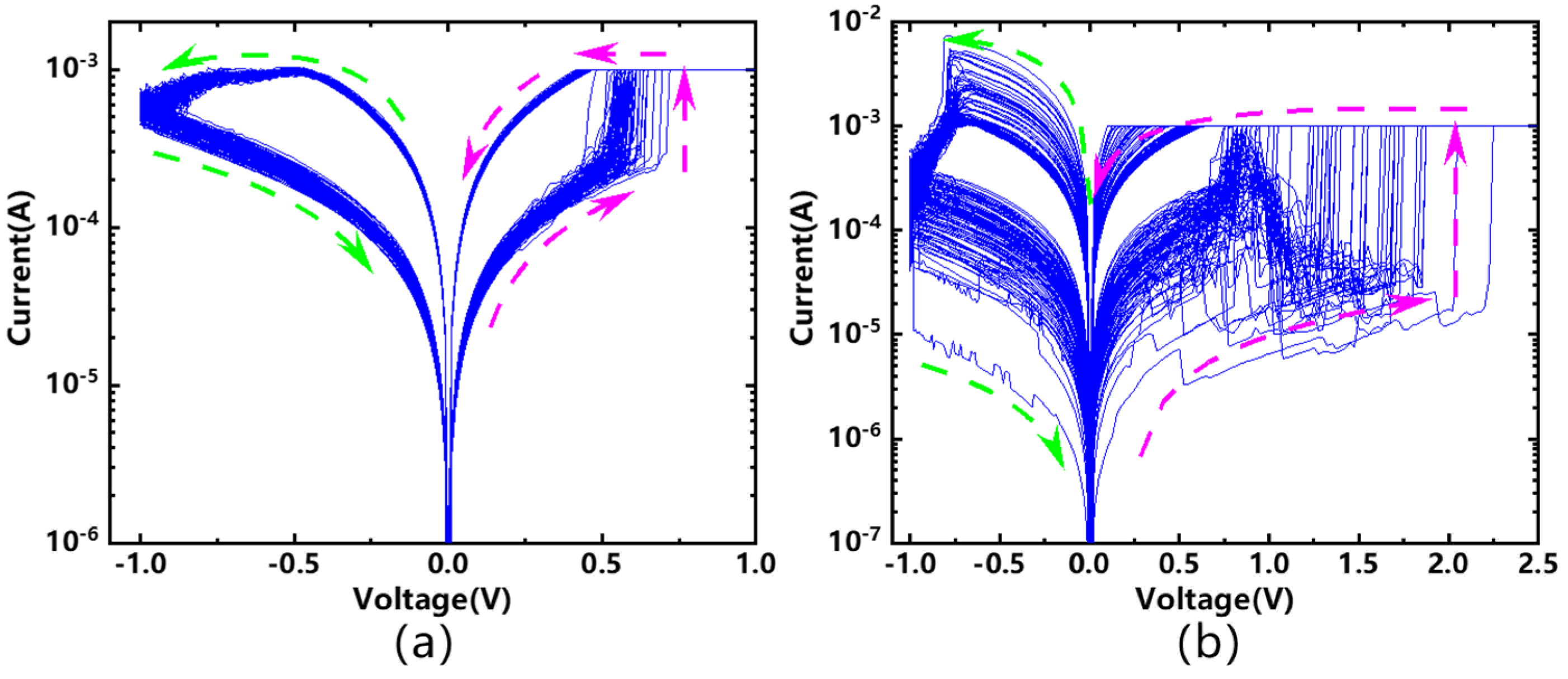
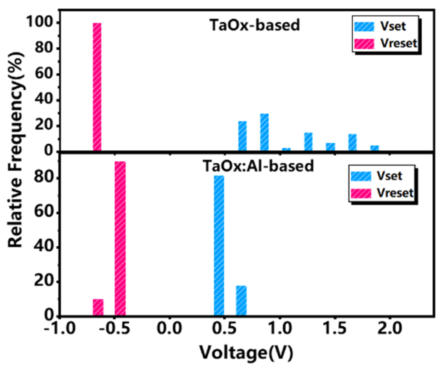
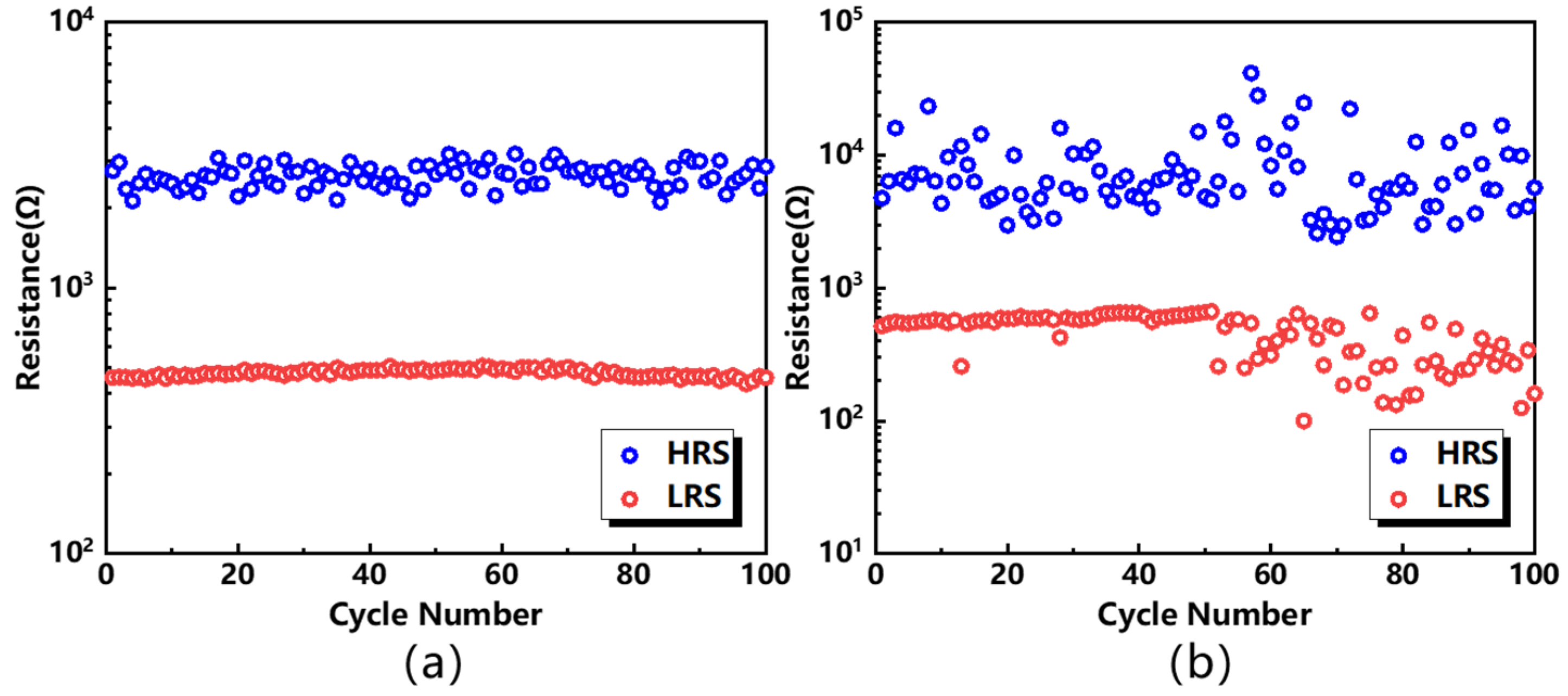
3.1. DC I-V Characteristics

The initial state of the device is a high resistance state (HRS). After forming, the device can be set to a low resistance state (LRS). Figure 2 shows the current-voltage (I-V) curves with 1 mA CC and −1 V reset stop voltage of the doped and undoped devices under 100 consecutive cycles. The set and reset process are marked by the magenta arrow and green arrow, respectively. Compared with the undoped device, the I-V curves of the Al ion locally doped device show excellent uniformity.
Figure 3 shows the set/reset voltage distribution of the undoped and locally doped devices with 100 cycles, respectively. The set voltage of the undoped device fluctuates significantly between 0.7 V and 1.9 V. In contrast, it can be found that the operating voltage distribution of the locally doped device is significantly tighter than that of the undoped device. Also, the set voltage (about 0.5~0.7 V) of the locally doped device is reduced compared to that of the undoped device, thus reducing the energy consumption of switching.
Figure 4 shows the distribution of HRS and LRS of the two devices after 100 cycles. The blue box and circle represent the resistance distribution of the undoped device. The red box and circle represent the resistance distribution of Al ion locally doped device. The distribution of HRS/LRS in the undoped device shows great fluctuation. The HRS range extends over an order of magnitude. The distribution of HRS and LRS in the locally doped device is quite uniform (the LRS is roughly 500 ohm, and the HRS is roughly 3000 ohm). Figure 5 shows the endurance of the Al ion locally doped device and the undoped device. The switching ratio of the devices is between 5 and 6. Local doping can not only reduce the cycle to cycle (C2C) variation of operating voltage and resistance states, but can also reduce the programming voltage. This is attributed to the decreased Vo formation energy after Al ion doping [34], which will be explained in detail later.

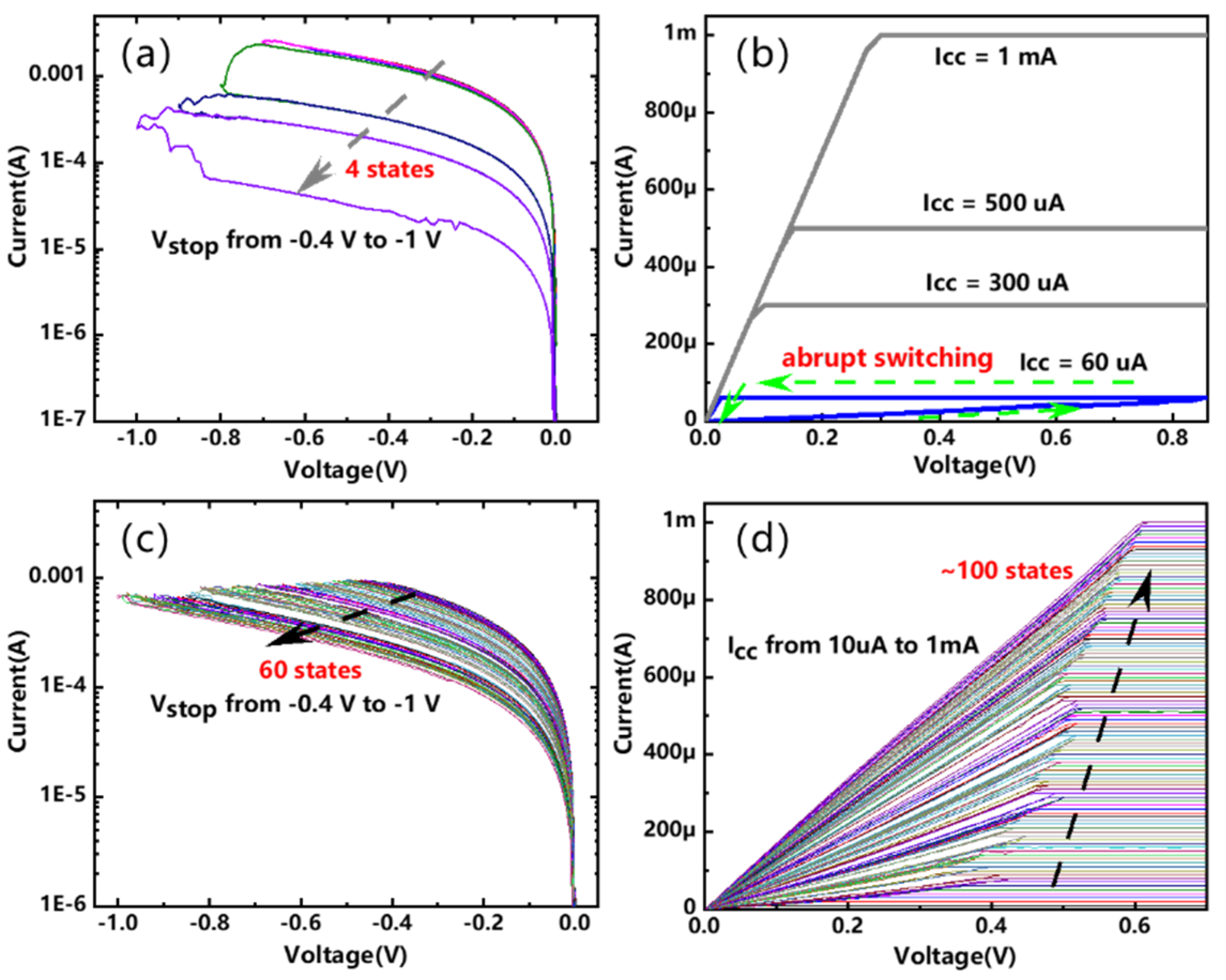
3.2. Analog Characteristics

We investigated the effect of Al ion doping on the analog characteristics of the device. Multi-level resistance states can be barely achieved either by gradually increasing the CC or adjusting the CC in the undoped device as shown in Figure 6a,b. It can be seen from Figure 6a that only 4 states can be obtained when the reset stop voltage increases from −0.4 V to −1 V with a step of −0.1 V. In other words, the undoped device has poor analog characteristics and cannot obtain multiple adjustable resistance states by increasing the CC. Figure 6c,d show the analog characteristics of the locally doped device. Excellent multi-level resistance states can be obtained by controlling the CC in the set process or the reset stop voltage in the reset process. Almost 100 resistance states can be obtained by increasing the CC with a 10 uA step. As shown in Figure 6c, 60 resistance states can be obtained by gradually increasing the reset stop voltage from −0.4 V to −1 V with a step of −0.01 V. A total of over 150 resistance states can be obtained in the Al ion locally doped device. It should be noted that more adjustable resistance states can be obtained by further refined voltage or CC parameters.
The Al ion locally doped device can be operated by identical pulses. As shown in Figure 7, the device exhibits long-term plasticity under consecutive 100 identical pulses with a read voltage of 0.1 V. The conductance can be gradually increased by 100 positive pulses (0.8 V, 20 ns) in the potentiation and decreased by 100 negative pulses (−1.1 V, 50 ns) in the depression. Large Gmax/Gmin (Gmax and Gmin are the maximum and minimum conductance during the potentiation and depression) and good linearity can be obtained in the TaOx-based RRAM with local doping.

3.3. Mechanism Explanation

The above test results show that the local doping of Al ions can not only reduce variation, but also improve analog properties. The generally accepted resistive switching mechanism of the TaOx-based RRAM is based on the generation and recombination of Vos, namely the filament model [42,43,44,45,46]. The migration of oxygen ions under the electric field in TaOx leads to a valence change between the TaO2 conducting phase and the Ta2O5 insulating phase [47,48]. The stochastic formation and the rupture of the Vo filament cause a large variation in the device’s characteristics. Doping Al ion can introduce more defects and decrease the formation energy of Vo, based on first-principles simulations [49]. Consequently, it is easier to form conductive filaments in the region with a high ion doping concentration, which helps to improve the uniformity of operating voltage distribution and resistance distribution. In the reset process, oxygen ions are driven by the electric field to return to the conductive filament and recombine with Vos to break the conductive filament. Therefore, the uniformity of reset voltage and HRS distribution are improved after Al ion doping. Because of the random ion implantation, the doping formed in the switching layer is not uniform. Reducing the area of the ion implantation region helps to increase the local ion doping concentration, so that Vos form at certain sites near Al dopants, and the formation and fracture of conductive filaments are limited to the ion implantation area. This contributes to reducing the variation of the size and location of conductive filaments. Therefore, local doping of Al ions can be adopted to improve the uniformity of the device.
The analog properties of the devices are also related to the migration of Vos. The accumulation of Vos leads to the evolution of a conductive filament in the undoped device during the set process, eventually resulting in a single strong conductive filament being formed in the switching layer. Therefore, the device without doping exhibits poor analog characteristics. However, local Al ion doping facilitates the formation and movement of Vos, thus contributing to the formation of multiple weak conductive filaments within the doping area. The analog switching behavior can be adjusted by increasing the CC and reset stop voltage. During the LTP/LTD process, the conductive filaments tend to gradually evolve to form or resolve the multiple conductive paths. Therefore, multi-level adjustable resistance states can be obtained in the locally doped device. As such, improved analog characteristics can be attributed to multiple weak conductive filaments in the local high Al ion doping region. The schematics of the switching mechanism on the Al ion locally doped device are demonstrated in Figure 8, where purple shaded area refers to the local Al ion doping area.

4. Conclusions

In this paper, we investigated the effect of the local doping of Al ions on a TaOx-based RRAM. The experimental results show that the device with local Al ion doping achieves excellent uniformity with tighter distribution of the operating voltage and resistance states. Moreover, the analog characteristics of the device are significantly improved through Al ion local doping. Multiple adjustable resistance states were obtained by controlling the set CC and reset stop voltage. In addition, the mechanism was analyzed to demonstrate the improved uniformity and analog properties of the device can be attributed to the formation of several weak conductive filaments in the local doping region. The improved uniformity and analog behavior of the device has great advantages in neuromorphic computing applications.

Author Contributions

Conceptualization, Y.Q. and Z.W.; validation, Y.Q. and Y.L.; investigation, Y.Q.; resources, Z.W., Y.C. and R.H.; data curation, Y.Q.; writing—original draft preparation, Y.Q.; writing—review and editing, Z.W. and Y.C.; supervision, Z.W. and Y.C.; project administration, Z.W. and Y.C.; funding acquisition, Z.W., Y.C. and R.H. All authors have read and agreed to the published version of the manuscript.

Funding

This work was supported by the National Key Research and Development Project of China under Grant 2018YFB1107701 and 2018YFE0203801 and the National Natural Science Foundation of China under Grant 61834001, Grant 62025401, Grant 61904003 and Grant 61421005, in part by the 111-project under Grant B18001, and in part by the Beijing Academy of Artificial Intelligence (BAAI).

Conflicts of Interest

The authors declare no conflict of interest.

References

  1. Yann, L.; Yoshua, B.; Geoffrey, H. Deep learning. Nature 2015, 521, 436–444. [Google Scholar]
  2. Zheng, Q.; Wang, Z.; Feng, Z.; Yan, B.; Cai, Y.; Huang, R.; Chen, Y.; Yang, C.L.; Li, H.H. Lattice: An ADC/DAC-less Re-RAM-based Processing-In-Memory Architecture for Accelerating Deep Convolution Neural Networks. In Proceedings of the 57th ACM/IEEE Design Automation Conference, San Francisco, CA, USA, 20–24 July 2020; pp. 1–6. [Google Scholar]
  3. Zhang, W.; Gao, B.; Tang, J.; Yao, P.; Yu, S.; Chang, M.F.; Yoo, H.J.; Qian, H.; Wu, H. Neuro-inspired computing chips. Nat. Electron. 2020, 3, 371–382. [Google Scholar] [CrossRef]
  4. Zhang, Z.; Wang, Z.; Shi, T.; Bi, C.; Rao, F.; Cai, Y.; Liu, Q.; Wu, H.; Zhou, P. Memory materials and devices: From concept to application. InfoMat 2020, 2, 261–290. [Google Scholar] [CrossRef] [Green Version]
  5. Bi, G.; Poo, M. Synaptic modifications in cultured hippocampal neurons: Dependence on spike timing, synaptic strength, and postsynaptic cell type. J. Neurosci. 1998, 18, 10464–10472. [Google Scholar] [CrossRef]
  6. Roy, K.; Jaiswal, A.; Panda, P. Towards spike-based machine intelligence with neuromorphic computing. Nature 2019, 575, 607–617. [Google Scholar] [CrossRef]
  7. Zheng, Q.; Wang, Z.; Gong, N.; Yu, Z.; Chen, C.; Cai, Y.; Huang, Q.; Jiang, H.; Xia, Q.; Huang, R. Artificial Neural Network Based on Doped HfO2 Ferroelectric Capacitors with Multilevel Characteristics. IEEE Electron Device Lett. 2019, 40, 1309–1312. [Google Scholar] [CrossRef]
  8. Wang, Z.; Zheng, Q.; Kang, J.; Yu, Z.; Zhong, G.; Ling, Y.; Bao, L.; Bao, S.; Bai, G.; Zheng, S.; et al. Self-Activation Neural Network based on Self-selective Memory Device with Rectified Multilevel States. IEEE Trans. Electron Devices 2020, 67, 4166–4171. [Google Scholar] [CrossRef]
  9. Upadhyay, N.K.; Jiang, H.; Wang, Z.; Asapu, S.; Xia, Q.; Yang, J.J. Emerging memory devices for neuromorphic computing. Adv. Mater. Technol. 2019, 4, 1800589. [Google Scholar] [CrossRef] [Green Version]
  10. Yang, J.J.; Strukov, D.B.; Stewart, D.R. Memristive devices for computing. Nat. Nanotechnol. 2013, 8, 13–24. [Google Scholar] [CrossRef]
  11. Jo, S.H.; Chang, T.; Ebong, I.; Bhadviya, B.B.; Mazumder, P.; Lu, W. Nanoscale memristor device as synapse in neuromorphic systems. Nano Lett. 2010, 10, 1297–1301. [Google Scholar] [CrossRef]
  12. Yu, M.; Fang, Y.; Wang, Z.; Chen, G.; Pan, Y.; Yang, X.; Yin, M.; Yang, Y.; Li, M.; Cai, Y.; et al. Encapsulation layer design and scalability in encapsulated vertical 3D RRAM. Nanotechnology 2016, 27, 205202. [Google Scholar] [CrossRef]
  13. Yao, P.; Wu, H.; Gao, B.; Tang, J.; Zhang, Q.; Zhang, W.; Yang, J.J.; Qian, H. Fully hardware-implemented memristor convolutional neural network. Nature 2020, 577, 641–646. [Google Scholar] [CrossRef]
  14. Yu, Z.; Wang, Z.; Kang, J.; Fang, Y.; Chen, Y.; Cai, Y.; Huang, R. Early-Stage Fluctuation in Low-Power Analog Resistive Memory: Impacts on Neural Network and Mitigation Approach. IEEE Electron Device Lett. 2020, 41, 940–943. [Google Scholar] [CrossRef]
  15. Ling, Y.; Wang, Z.; Fang, Y.; Kang, J.; Wu, L.; Yang, Y.; Cai, Y.; Huang, R. RTN impacts on RRAM-based Nonvolatile logic circuit. In Proceedings of the IEEE International Conference on Solid-State and Integrated Circuit Technology, Qingdao, China, 31 October–3 November 2018; pp. 1–3. [Google Scholar]
  16. Kang, J.; Yu, Z.; Wu, L.; Fang, Y.; Wang, Z.; Cai, Y.; Ji, Z.; Zhang, J.; Wang, R.; Yang, Y.; et al. Time-Dependent Variability in RRAM-based Analog Neuromorphic System for Pattern Recognition. In Proceedings of the IEEE International Electron Devices Meeting, San Francisco, CA, USA, 2–6 December 2017; pp. 6.4.1–6.4.4. [Google Scholar]
  17. Zhao, M.; Gao, B.; Tang, J.; Qian, H.; Wu, H. Reliability of analog resistive switching memory for neuromorphic computing. Appl. Phys. Rev. 2020, 7, 011301. [Google Scholar] [CrossRef]
  18. Cai, Y.; Wang, Z.; Yu, Z.; Ling, Y.; Chen, Q.; Yang, Y.; Bao, S.; Wu, L.; Bao, L.; Wang, R.; et al. Technology-Array-Algorithm Co-Optimization of RRAM for Storage and Neuromorphic Computing: Device Non-idealities and Thermal Cross-talk. In Proceedings of the IEEE International Electron Devices Meeting, San Francisco, CA, USA, 12–18 December 2020; pp. 13.4.1–13.4.4. [Google Scholar]
  19. Gao, B.; Zhang, H.W.; Yu, S.; Sun, B.; Liu, L.; Wang, Y.; Han, R.Q.; Kang, J.F.; Yu, B.; Wang, Y.Y. Oxide-based RRAM: Uniformity improvement using a new material-oriented methodology. In Proceedings of the 2009 Symposium on VLSI Technology, Kyoto, Japan, 15–17 June 2009; pp. 30–31. [Google Scholar]
  20. Liu, Y.; Cai, Y.; Li, Q.; Pan, Y.; Wang, Z.; Huang, R. Inorganic-organic hybrid resistive switching memory with high uniformity and multilevel operation. In Proceedings of the International Symposium on VLSI Technology, Systems and Application, Hsinchu, Taiwan, 28–30 April 2014; pp. 1–2. [Google Scholar]
  21. Wong, H.S.P.; Lee, H.Y.; Yu, S.; Chen, Y.S.; Wu, Y.; Chen, P.S.; Lee, B.; Chen, F.T.; Tsai, M.J. Metal–oxide RRAM. Proc. IEEE 2012, 100, 1951–1970. [Google Scholar] [CrossRef]
  22. Li, X.; Zhang, B.; Wang, B.; Xu, X.; Yang, Y.; Sun, S.; Cai, Q.; Hu, S.; An, X.; Li, M.; et al. Low power and high uniformity of HfOx-based RRAM via tip-enhanced electric fields. Sci. China-Inf. Sci. 2019, 10, 1–7. [Google Scholar] [CrossRef] [Green Version]
  23. Choi, S.; Tan, S.H.; Li, Z.; Kim, Y.; Choi, C.; Chen, P.Y.; Yeon, H.; Yu, S.; Kim, J. SiGe epitaxial memory for neuromorphic computing with reproducible high performance based on engineered dislocations. Nat. Mater. 2018, 17, 335–340. [Google Scholar] [CrossRef]
  24. Zhang, H.; Liu, L.; Gao, B.; Qiu, Y.; Liu, X.; Lu, J.; Han, R.; Kang, J.; Yu, B. Gd-doping effect on performance of HfO2 based resistive switching memory devices using implantation approach. Appl. Phys. Lett. 2011, 98, 042105. [Google Scholar] [CrossRef]
  25. Liu, Q.; Long, S.; Wang, W.; Zuo, Q.; Zhang, S.; Chen, J.; Liu, M. Improvement of Resistive Switching Properties in ZrO2-Based ReRAM With Implanted Ti Ions. IEEE Electron Device Lett. 2009, 30, 1335–1337. [Google Scholar] [CrossRef]
  26. Xie, H.; Liu, Q.; Li, Y.; Lv, H.; Wang, M.; Liu, X.; Sun, H.; Yang, X.; Long, S.; Liu, S.; et al. Nitrogen-induced improvement of resistive switching uniformity in a HfO2-based RRAM device. Semicond. Sci. Technol. 2012, 27, 125008. [Google Scholar] [CrossRef]
  27. Guan, W.; Long, S.; Liu, Q.; Liu, M.; Wang, W. Nonpolar Nonvolatile Resistive Switching in Cu Doped ZrO2. IEEE Electron Device Lett. 2008, 29, 434–437. [Google Scholar] [CrossRef]
  28. Duncan, D.; Magyari-Köpe, B.; Nishi, Y. Properties of Dopants in HfOx for Improving the Performance of Nonvolatile Memory. Phys. Rev. Appl. 2017, 7, 034020. [Google Scholar] [CrossRef]
  29. Fang, Y.; Yu, Z.; Wang, Z.; Zhang, T.; Yang, Y.; Cai, Y.; Huang, R. Improvement of HfOx-Based RRAM Device Variation by Inserting ALD TiN Buffer Layer. IEEE Electron Device Lett. 2018, 39, 819–822. [Google Scholar] [CrossRef]
  30. Fang, Z.; Yu, H.Y.; Li, X.; Singh, N.; Lo, G.Q.; Kwong, D.L. HfOx/TiOx/HfOx/TiOx Multilayer-Based Forming-Free RRAM Devices with Excellent Uniformity. IEEE Electron Device Lett. 2011, 32, 566–568. [Google Scholar] [CrossRef]
  31. Sun, Y.; Xu, H.; Wang, C.; Song, B.; Liu, H.; Liu, Q.; Liu, S.; Li, Q. A Ti/AlOx/TaOx/Pt analog synapse for memristive neural network. IEEE Electron Device Lett. 2018, 39, 1298–1301. [Google Scholar] [CrossRef]
  32. Wang, Z.; Kang, J.; Yu, Z.; Fang, Y.; Ling, Y.; Cai, Y.; Huang, R.; Wang, Y. Modulation of non-linear resistive switching behavior of TaOx-based resistive device through interface engineering. Nanotechnology 2017, 28, 055204. [Google Scholar] [CrossRef]
  33. Chuang, K.C.; Chu, C.Y.; Zhang, H.X.; Luo, J.D.; Li, W.S.; Li, Y.S.; Cheng, H.C. Impact of the stacking order of HfOx and AlOx dielectric films on RRAM switching mechanisms to behave digital resistive switching and synaptic characteristics. IEEE J. Electron Devices Soc. 2019, 7, 589–595. [Google Scholar] [CrossRef]
  34. Wang, Z.; Kang, J.; Fang, Y.; Yu, Z.; Yang, X.; Cai, Y.; Wang, Y.; Huang, R. Localized metal doping effect on switching behaviors of TaOx-based RRAM device. In Proceedings of the 16th Non-Volatile Memory Technology Symposium, Pittsburgh, PA, USA, 17–19 October 2016; pp. 1–3. [Google Scholar]
  35. Xi, Y.; Gao, B.; Tang, J.; Chen, A.; Chang, M.F.; Hu, X.S.; Van Der Spiegel, J.; Qian, H.; Wu, H. In-memory learning with analog resistive switching memory: A review and perspective. Proc. IEEE 2020, 109, 14–42. [Google Scholar] [CrossRef]
  36. Gao, B.; Wu, H.; Wu, W.; Wang, X.; Yao, P.; Xi, Y.; Zhang, W.; Deng, N.; Huang, P.; Liu, X.; et al. Modeling disorder effect of the oxygen vacancy distribution in filamentary analog RRAM for neuromorphic computing. In Proceedings of the IEEE International Electron Devices Meeting, San Francisco, CA, USA, 2–6 December 2017; pp. 4.4.1–4.4.4. [Google Scholar]
  37. Wang, Z.; Yin, M.; Zhang, T.; Cai, Y.; Wang, Y.; Yang, Y.; Huang, R. Engineering incremental resistive switching in TaOx based memristors for brain-inspired computing. Nanoscale 2016, 8, 14015–14022. [Google Scholar] [CrossRef]
  38. Sun, B.; Liu, Y.X.; Liu, L.F.; Xu, N.; Wang, Y.; Liu, X.Y.; Han, R.Q.; Kang, J.F. Highly uniform resistive switching characteristics of TiN/ZrO2/Pt memory devices. J. Appl. Phys. 2009, 105, 061630. [Google Scholar] [CrossRef]
  39. Fujimoto, M.; Koyama, H.; Konagai, M.; Hosoi, Y.; Ishihara, K.; Ohnishi, S.; Awaya, N. TiO2 anatase nanolayer on TiN thin film exhibiting high-speed bipolar resistive switching. Appl. Phys. Lett. 2006, 89, 223509. [Google Scholar] [CrossRef]
  40. Yoshida, C.; Tsunoda, K.; Noshiro, H.; Sugiyama, Y. High speed resistive switching in Pt/TiO2/TiN film for nonvolatile memory application. Appl. Phys. Lett. 2007, 91, 223510. [Google Scholar] [CrossRef]
  41. Sun, C.; Lu, S.M.; Jin, F.; Mo, W.Q.; Song, J.L.; Dong, K.F. Control the switching mode of Pt/HfO2/TiN RRAM devices by tuning the crystalline state of TiN electrode. J. Alloy. Compd. 2018, 749, 481–486. [Google Scholar] [CrossRef]
  42. Prakash, A.; Deleruyelle, D.; Song, J.; Bocquet, M.; Hwang, H. Resistance controllability and variability improvement in a TaOx-based resistive memory for multilevel storage application. Appl. Phys. Lett. 2015, 106, 233104. [Google Scholar] [CrossRef] [Green Version]
  43. Kim, K.M.; Lee, S.R.; Kim, S.; Chang, M.; Hwang, C.S. Self-limited switching in Ta2O5/TaOx memristors exhibiting uniform multilevel changes in resistance. Adv. Funct. Mater. 2015, 25, 1527–1534. [Google Scholar] [CrossRef]
  44. Chen, J.Y.; Huang, C.W.; Chiu, C.H.; Huang, Y.T.; Wu, W.W. Switching kinetic of VCM-based memristor: Evolution and positioning of nanofilament. Adv. Mater. 2015, 27, 5028–5033. [Google Scholar] [CrossRef]
  45. Lee, M.J.; Lee, C.B.; Lee, D.; Lee, S.R.; Chang, M.; Hur, J.H.; Kim, Y.B.; Kim, C.J.; Seo, D.H.; Seo, S.; et al. A fast, high-endurance and scalable non-volatile memory device made from asymmetric Ta2O5−x/TaO2−x bilayer structures. Nat. Mater. 2011, 10, 625–630. [Google Scholar] [CrossRef]
  46. Ninomiya, T.; Muraoka, S.; Wei, Z.; Yasuhara, R.; Katayama, K.; Takagi, T. Improvement of Data Retention During Long-Term Use by Suppressing Conductive Filament Expansion in TaOx Bipolar-ReRAM. IEEE Electron Device Lett. 2013, 34, 762–764. [Google Scholar] [CrossRef]
  47. Wei, Z.; Kanzawa, Y.; Arita, K.; Katoh, Y.; Kawai, K.; Muraoka, S.; Mitani, S.; Fujii, S.; Katayama, K.; Iijima, M.; et al. Highly reliable TaOx ReRAM and direct evidence of redox reaction mechanism. In Proceedings of the IEEE International Electron Devices Meeting, San Francisco, CA, USA, 15–17 December 2008; pp. 1–4. [Google Scholar]
  48. Wei, Z.; Takagi, T.; Kanzawa, Y.; Katoh, Y.; Ninomiya, T.; Kawai, K.; Muraoka, S.; Mitani, S.; Katayama, K.; Fujii, S.; et al. Demonstration of high-density ReRAM ensuring 10-year retention at 85 C based on a newly developed reliability model. In Proceedings of the IEEE International Electron Devices Meeting, San Francisco, CA, USA, 5–7 December 2011; pp. 31.4.1–31.4.4. [Google Scholar]
  49. Deng, H.; Cai, Y.; Yu, M.; Huang, R. Formation Energy Study of Oxygen Vacancies in Undoped, Aluminum-Doped and Nitrogen-Doped TaOx-Based RRAM by First Principle Simulation. ECS Trans. 2014, 60, 15. [Google Scholar] [CrossRef]
Figure 1. (a) The structure diagram of Pt/TaOx:Al/TiN RRAM; (b) SEM image of TaOx-based RRAM with Al ion local doping.
Electronics 10 02451 g001
Figure 2. 100 consecutive I-V curves with 1 mA CC and −1 V reset stop voltage of (a) Pt/TaOx:Al/TiN RRAM and (b) Pt/TaOx/TiN RRAM.
Electronics 10 02451 g002
Figure 3. Cycle to cycle distributions of set/reset voltage of the undoped (top) and locally doped devices (bottom).
Electronics 10 02451 g003
Figure 4. Distribution of HRS and LRS for the undoped (blue) and locally-doped Al ion devices (red) after 100 cycles of scanning.
Electronics 10 02451 g004
Figure 5. Endurance of HRS and LRS over 100 cycles for (a) Pt/TaOx:Al/TiN RRAM and (b) Pt/TaOx/TiN RRAM.
Electronics 10 02451 g005
Figure 6. Comparison of DC analog characteristics for Pt/TaOx/TiN RRAM and Pt/TaOx:Al/TiN RRAM. (a) Gradual reset process of Pt/TaOx/TiN RRAM. Four states can be obtained with reset stop voltage increasing from −0.4 V to −1 V with a step of −0.1 V. (b) Abrupt set process of Pt/TaOx/TiN RRAM. The undoped device has been tuned by increasing set CC repeatedly, and representative I-V curves with set CC (60 uA, 300 uA, 500 uA and 1 mA) are shown here for the sake of illustration. An obvious switching window appears at 60 uA CC, and the device cannot be tuned gradually to LRS, with CC increasing to 1 mA. Over 150 resistance states can be achieved in Pt/TaOx:Al/TiN RRAM through (c) increasing reset stop voltage from −0.4 V to −1 V with a step of −0.01 V and (d) increasing CC gradually from 10 uA to 1 mA with a step of 10 uA.
Electronics 10 02451 g006
Figure 7. Long-term potentiation (LTP) and depression (LTD) of Pt/TaOx:Al/TiN RRAM with 100 optimized identical (a) positive pulses (0.8 V, 20 ns) and (b) negative pulses (−1.1 V, 50 ns).
Electronics 10 02451 g007
Figure 8. The schematics of the complete switching mechanism of Pt/TaOx:Al/TiN RRAM.
Electronics 10 02451 g008
Publisher’s Note: MDPI stays neutral with regard to jurisdictional claims in published maps and institutional affiliations.

