1. Introduction
The exponential rise in the demand for a high data rate in cellular and WLAN communications requires the current systems to demonstrate their capability to handle the upcoming throughput requirements. In order to deal with this challenge, shifting the systems to higher frequency bands in the spectrum is the only viable solution. A significant module in wireless systems is the power amplifier (PA). Integrated power amplifiers operable at microwave/millimeter-wave frequencies focusing 5G-communications are expected to demonstrate high efficiency and wideband operation within a small form factor. In a transceiver system, the power amplifier is the most dissipative module, which consumes power from the system’s battery. Hence, in order to extend the battery life in portable devices, it is imperative to design a power amplifier that demonstrates a high power efficiency [
1,
2,
3,
4,
5]. Moreover, recently, the Federal Communications Commission (FCC) has also emphasized maximizing the battery life of the client device operating at the new unlicensed 6 GHz band (5.925 GHz to 7.125 GHz) [
5]. Therefore, there is a crucial need for a 6 GHz power amplifier that exhibits high efficiency and thereby improves the battery life of the client device.
“Single-Transistor” PAs are desirable for 5G-mobile communications as they offer low-voltage operation, a small form factor, and a high power-added efficiency (PAE) if the PA is harmonically tuned. Moreover, the “single-transistor” approach incurs lower power consumption and, hence, naturally exhibits superior power efficiency over the multi-transistor approach (e.g., cascode or stacked, etc.). The term “single-transistor” means transistors are merged (shunted) in a parallel combination but are represented as one device in the circuit. “Single-transistor” integrated Class-F/F
−1 power amplifiers operable at “5G-millimeter-wave frequencies” have been investigated in recent years. However, an integrated “single-transistor” Class-F/F
−1 power amplifier operable at a “5G-microwave frequency” of 6 GHz has not been reported so far in the literature. A single-transistor millimeter-wave Class-F/F
−1 power amplifier in SiGe-BiCMOS was reported in [
6]. This power amplifier employed a wave-shaping network connected at the collector node of the active device, which allows it to transform from Class-F
−1 to Class-F when the frequency shifts from 24 GHz to 31 GHz. The amplifier was operating at 2.2 V and delivered 40.7% PAE along with a gain of 10.3 dB and an output power of 17.1 dBm. Very recently, a 65 nm CMOS single-transistor Class-F power amplifier operable at 5G-millimeter-wave frequencies was reported in [
7]. The 1.1 V driven power amplifier rendered 46.4% peak PAE, a power gain of 10 dB along with an output power of around 14.75 dBm. To the best of the author’s knowledge, this paper reports the first “single-transistor” integrated Class-F
−1 power amplifier operable at a “5G-microwave frequency” of 6 GHz. The amplifier is designed in 65 nm CMOS technology. The proposed design employs a “parasitic-aware” Class-F
−1 harmonic control network connected at the drain terminal of the NMOS device. There are several Class-F
−1 circuit topologies based on the LC network [
6,
7,
8,
9,
10]; however, the proposed Class-F
−1 LC-network is a new topology deduced using a novel iterative algorithm. A dual-purpose output matching network is incorporated in the design, which reinforces the waveform-shaping capability of the Class-F
−1 harmonic network along with performing the typical task of output impedance matching. The proposed amplifier offers one of the highest PAEs (47.8%) compared to many other monolithic microwave/millimeter-wave CMOS and SiGe power amplifiers reported so far.
This paper is organized as follows.
Section 2 describes the details of the Class-F
−1 amplifier’s circuit topology, which includes a harmonic control network and dual-purpose output matching circuit. Moreover, the section also explains in detail the iterative algorithm employed to extract the component values of the harmonic network. Measurement results and a comparison table are reported in
Section 3. Finally,
Section 4 concludes the work presented in this paper.
2. Single-Transistor Class-F−1 Power Amplifier
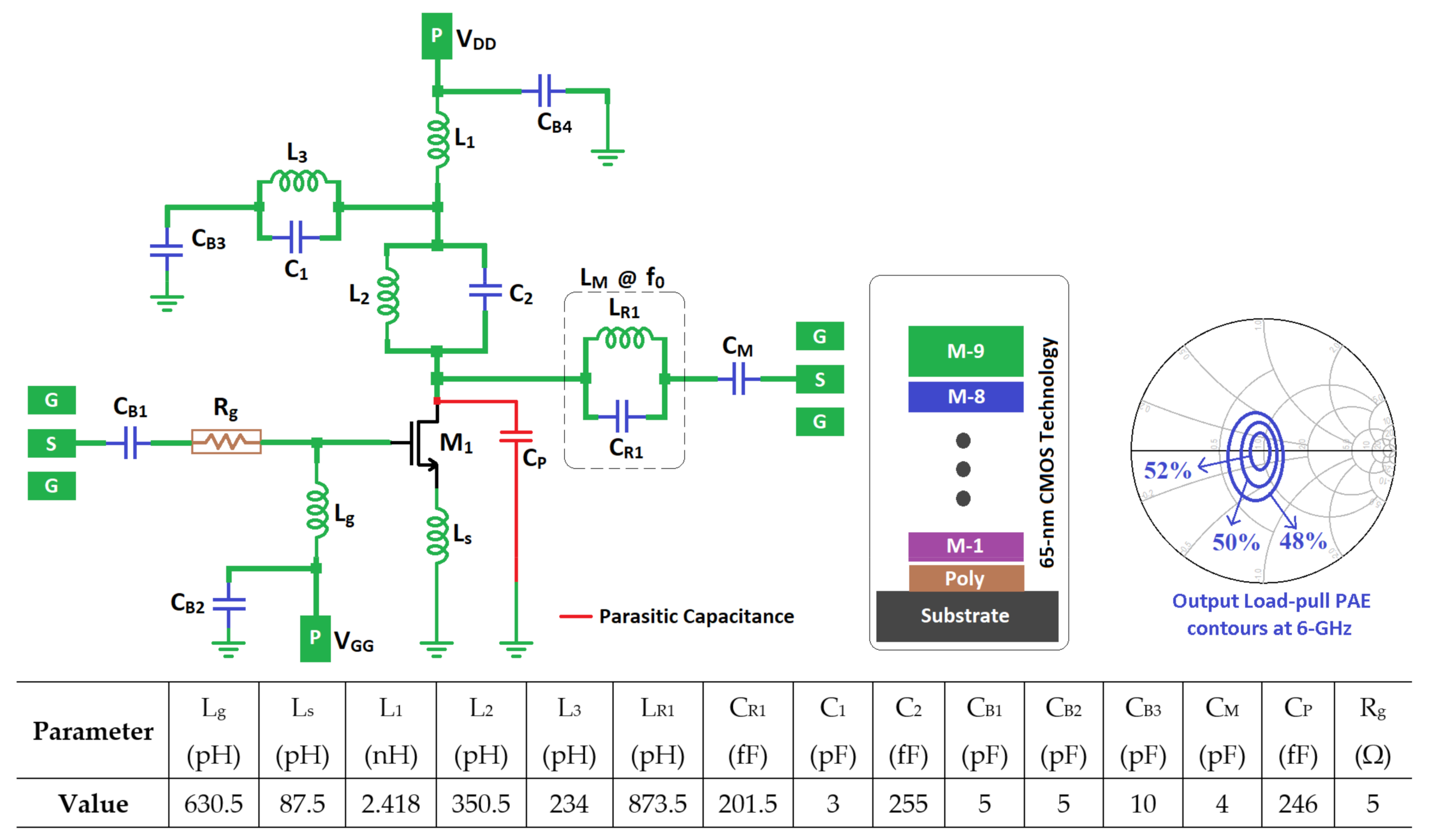
Figure 1 shows the proposed Class-F
−1 PA using a “single-transistor” approach, implemented in 65 nm TSMC CMOS technology. The active device in the design employs an NMOS transistor M
1. The total width of the device (W
T) is 384 µm, which is divided into six power-cell units. Each power-cell unit contains 32 fingers (N
f), and each finger is 2 µm wide (W
f). The amplifier is biased, with a drain supply V
DD of 1.1 V and gate supply V
GG of 480 mV. A 5 Ω resistor (R
g) and a small inductor (L
s) are incorporated, respectively, at the gate and at the source of the transistor for the purpose of establishing unconditional stability for the power amplifier.
The drain terminal is loaded with a novel “parasitic-aware” Class-F−1 harmonic control network, which harvests the parasitic capacitance CP (246 fF) in its implementation. The parallel resonant tank (L2, C2) behaves as an inductor at the fundamental frequency f0, and combines its inductance with L1 to tune out the parasitic capacitance CP. However, the tank circuit (L3, C1) resonates at f0 to create an open circuit, and, hence, does not interrupt the fundamental frequency’s path to resonate out the CP. At the second harmonic frequency 2f0, the resonant tank (L2, C2) acts again as an inductor, which resonates out the parasitic capacitance CP. However, the tank circuit (L3, C1) becomes overall capacitive at 2f0 and constitutes a low impedance path to the ground, thereby discarding the presence of the inductor L1 and leaving the second harmonic to resonate with the remaining circuit, whereas at 3f0, the tank (L2, C2) becomes capacitive and constitutes a series LC resonant circuit with the inductor L1 resulting in the formation of a short circuit path to the AC ground. A second short circuit path for the third harmonic is also established by the tank circuit (L3, C1), which behaves as an overall capacitor, thus dumping 3f0 into ground. Hence, with the help of this passive frequency-steering the employed harmonic network accomplishes the requirements for Class-F−1 loading.
In order to determine the values of the inductors (L
1, L
2) and the capacitor C
2, a novel “educated” and deterministic iterative technique is employed. It begins by inserting an incremental capacitance value, ΔC in (1) in each k
th iteration step of contiguous steps and then executing and validating a sequence of equations in a loop to finally extract the required reactive component values. The following equations are loaded in MATLAB in a routine and then the values of the components C
2, L
1, and L
2 are extracted instantly at the end of the iterative search.
where [ΔC]
k is an incremental value in fF (such as 1fF, 3fF, 7fF, etc.) at the kth step, with k = 1, 2, 3….n. Additionally, in the equations below, f
1o, f
2o, and f
3o are the fundamental, 2nd and 3rd harmonics of the 6 GHz microwave center frequency, while f
0R, f
2R, and f
3R are the calculated resonance frequencies in each iteration. In addition, L
eq@2fo and X
Leq@2fo are, respectively, the required equivalent inductance and the corresponding inductive reactance of the parallel resonant tank (L
2, C
2) to tune out C
P at the 2nd harmonic. Further, X
Ceq@3fo and C
eq@3fo are, respectively, the equivalent capacitive reactance and the corresponding equivalent capacitance of the tank (L
2, C
2) at the 3rd harmonic. Finally, X
Leq@fo and L
eq@fo are, respectively, the equivalent inductive reactance and the corresponding equivalent inductance of the tank (L
2, C
2) at the fundamental frequency. The parasitic “C
P” thus provides the starting “educated” search reference for C
2, while L
1 and L
2 are found deterministically using C
2. It is thus different from any “brute force” algorithm, which may employ roughly estimated trial values. Now, for this proposed iterative technique:
Since the parameters CP = 246 fF (captured through parasitic extraction incorporating the transistor’s parasitic capacitance (Cds) plus parasitics associated with the layout interconnects), f1o = 6 GHz, f2o = 12 GHz, and f3o = 18 GHz are known, they are used to extract the required component values by employing the above iterative technique.
It can be seen from the above equations and
Table 1 that the required resonance conditions at the 2nd and 3rd harmonics (f
2R and f
3R) are automatically in agreement, and satisfaction of the resonance condition at the fundamental, f
0R, is the validating parameter in this iterative component extraction method. For the first three iteration values of ΔC, the deduced reactive components resonate close to f
0R, but for the last iteration value of ΔC (=9fF), f
0R comes exactly to 6 GHz thereby completing the component search. It can be noted that the proposed algorithm starts from a specific reference value and quickly converges to the solution, as shown in the table. It is judiciously designed around a single parameter, i.e., a parasitic capacitance, and, hence, is different from other optimization algorithms, which perform a search based on arbitrary values of the various parameters.
Determining the component values of the tank circuit (L
3, C
1) constitutes a separate sub-problem and have been evaluated for resonance at f
0 and for equivalent capacitive AC-bypass to ground at 2f
0 and 3f
0. Hence, setting C
1 to a suitable value of 3 pF, L
3 can be easily deduced as follows:
For the purpose of satisfying the Class-F
−1 condition, the output-matching network also has to present an open-circuit to the second harmonic so that this harmonic would reflect back towards the drain of the active device. A simple output-impedance matching can be established by just using the two components, inductor L
M and capacitor C
M; however, in order to stop the second harmonic from propagating towards the load, a simple technique is employed. In this technique, the inductor L
M (1.165 nH) is judiciously decomposed into a 2f
0-tank circuit by employing the design equations below:
The above-mentioned design equations can be used to convert any inductor into a 2f0-tank-circuit. The tank-circuit (LR1, CR1) offers an open-circuit to the second-harmonic and behaves as the inductor LM at the fundamental. Hence, the proposed output-matching network adds the second harmonic content at the NMOS drain terminal. This causes further refinement in the voltage waveform, resulting in a reduction in the current–voltage overlap and, hence, improving the power-added efficiency.
The proposed Class-F
−1 harmonic control network, along with the dual-purpose output-matching network connected at the drain of the NMOS transistor, performs the desired wave-shaping operation as shown in
Figure 2. The voltage waveform approximates itself as a half-sinusoidal wave as the second harmonic content is dominant, whereas the current waveform is approximating itself as a square wave due to the higher third harmonic content (
Figure 3). Load impedance observed from the drain terminal of the NMOS device (
Figure 4) maintains a constant impedance close to the optimum value of 50 Ω at the fundamental frequency (f
0). The impedance trace depicts a high impedance at the second harmonic frequency (2f
0) and low impedance at the third harmonic frequency (3f
0). The input impedance matching is realized with the help of a DC-blocking capacitor, C
B1, as shown in
Figure 1. The output load-pull simulations of the power amplifier offer around 52% peak PAE at 6 GHz, as indicated by the contours on the Smith chart in
Figure 1.
3. Measurement Results
Figure 5 shows the photomicrograph of the implemented power amplifier employing the 65 nm TSMC CMOS process with a PA size of 753 µm × 927 µm. A Cascade Micro-Tech Summit 11K probe-station along with infinity-quad-probe (50 GHz RF and 100-µm pitch) and a Rohde & Schwarz ZVA50 Vector Network Analyzer employed for on-wafer testing, as shown in
Figure 5. Standard SOLT calibration was performed for the purpose of on-wafer small-signal S-parameter measurements with the results shown in
Figure 6. The measured S
11 and S
22 values are under −10 dB for a considerable range of frequencies of interest. The measured maximum S
21 was 14.1 dB along with a −3 dB range of 3.67–7.4 GHz, thus offering a 3.7 GHz wide small-signal bandwidth (BW
3dB = 67.4%). Stability analysis reveals that the amplifier’s stability factor (k) is greater than 1, as shown in
Figure 7, ensuring unconditional stability of the proposed power amplifier.
Large signal measurements were conducted with the help of a power meter and power sensors. The measured results captured at the operating frequency of 6 GHz are shown in
Figure 8. The amplifier exhibits a peak power-added efficiency (PAE) of 47.8%, saturated output power, P
SAT, of 14.4 dBm and, a power gain of 13.8 dB. The output power at the 1 dB compression point, OP
−1dB, is 12.9 dBm.
Figure 9 shows the measured PAE traces from 5 GHz to 7 GHz with respect to the input power. P
OUT stays above 12 dBm from 3.5 GHz to 7.5 GHz, whereas PAE remains higher than 30% from 4 GHz to 7.5 GHz, as shown in
Figure 10. Normalized AM–AM and AM–PM distortion curves are depicted in
Figure 11. The measured AM–PM distortion at P
in, −1dB (6 dBm) is less than 2°, indicating good linearity performance.
Table 2 compares the proposed PA with several previously reported PAs in CMOS and SiGe. It can be easily inferred from
Table 2 that the proposed amplifier yields the highest peak PAE (47.8%) as compared to the referenced papers. According to the author’s knowledge, there are no “single-transistor” integrated microwave Class-F/F
−1 PAs that have been reported so far; however, two millimeter-wave Class-F/F
−1 PAs with similar “single-transistor architecture” have been reported, and these have been included in the table, although they are in a totally different RF spectrum compared to the other PAs in the table. The proposed PA offers a very high efficiency and operationwise reasonable output power. The saturated output power of 14.4 dBm resides within the designated power limits outlined by the FCC [
5] for establishing 5G communications at 6 GHz. Moreover, this power level helps to extend the client device battery life as well.
Table 2 also shows that when compared to other 6 GHz power amplifiers, the proposed PA offers low-voltage operation (1.1 V) and small form factor.


