Abstract
In this paper, a new analytical design technique for a three-section wideband Wilkinson power divider is presented. The proposed design technique utilizes the dual-frequency behavior of commensurate transmission lines for the even-mode analysis and contributes a set of completely new and rigorous design equations for the odd-mode analysis. Measurement of a fabricated prototype utilizing the proposed technique shows an excellent return-loss (>16 dB), insertion loss (<3.35 dB), and excellent isolation (>22.7 dB) over 104% fractional bandwidth extending beyond the minimum requirements.
1. Introduction
Power dividers are indispensable and ubiquitous components in radio-frequency (RF)/microwave systems [1,2]. For example, they are frequently used in antenna feeding networks, multistage and Doherty power amplifiers, mixers, and in RF/microwave measurements. Owing to their ability to provide decent matching and isolation in a simpler structure, the three-port Wilkinson power divider (WPD) has become one of the most widely used power divider types [3]. Due to their importance, there is an abundance of reports in the literature on the design and development of WPDs. Recent advancements in high-data-rate wireless communication systems have refueled significant interest in the development of power dividers with a major research focus on wideband, harmonic-suppressed, and multi-band topologies [2,4,5,6].
The conventional multi-section WPD was designed by using the theory reported in [3], which is a fully analytical technique applied only to a two-section WPD. For three or more sections, the reported technique is actually a table-based design and is therefore less computer-friendly. In addition, for this conventional design for a bandwidth, BW = , the reflection profile appears as the one shown in Figure 1a, with being the mid-band frequency and is the minimum return-loss in dB. In this paper, a fully analytical design approach is presented for a three-section WPD that can be easily implemented using a computational tool, such as MATLAB/Octave. In addition, as depicted in Figure 1b, the proposed design methodology utilizes a dual-band design concept [7] to arrive at a wideband design. This dual-band design approach guarantees that the resonance frequencies are always located at and , and therefore, the achieved BW , where is the extra bandwidth that provides a margin for process/component variations. This approach is the usual choice for a commercial development setup, where the minimum bandwidth requirement will always be met, and will allow flexibility to meet design goal requirements.
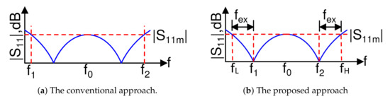
Figure 1.
The conventional vs. the proposed design methodologies.
2. The Three-Section WPD and the Proposed Design Equations
The classic three-section 3 dB WPD is depicted in Figure 2. P1 refers to the input port, whereas P2 and P3 are the two output ports. Each port has a termination impedance of . Further, , , and are the characteristic impedances of three transmission lines, while refers to their electrical length. Finally, , , and are the isolation resistors connected as shown in the Figure. Since the structure is fully symmetric about a horizontal axis passing through P1, the widely known even-odd mode analysis technique is utilized to perform its analysis.
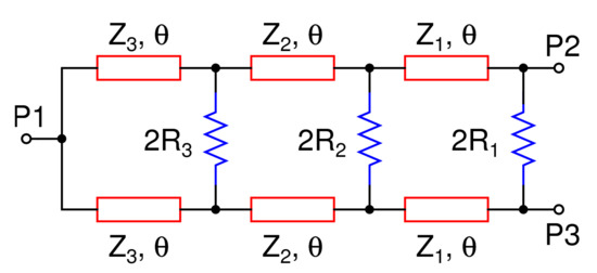
Figure 2.
The three-section WPD.
2.1. Even-Mode Analysis
The even-mode equivalent circuit is shown in Figure 3a which has been obtained after bisecting the network of Figure 2. In the even mode excitation, two equal voltage generators with the same polarity are connected to P2 and P3, hence no current flows through the resistors, and thus the plane of symmetry becomes a virtual open. It is apparent that this equivalent circuit is in fact a special case of multi-section commensurate transmission lines discussed in [7]. To formulate the expression of and , we can refer to similar equations as shown in [7], which were derived for the three-section transmission line. Now, by considering a source impedance of and a load impedance of , we can obtain the following:
where and a = tan
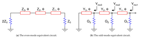
Figure 3.
The even- and odd-mode equivalent circuits of the three-section WPD.
The value of is obtained by solving the fourth-order equation in given by:
where
Out of the four roots of obtained from (2) using MATLAB, only the positive real roots will be considered, which in turn will be used to find from (1). The design consideration for choosing is outlined in Section 3. Finally, as explained in [7], at for a dual-band design is chosen as:
2.2. Odd-Mode Analysis
The odd-mode equivalent circuit is shown in Figure 3b, which has been obtained after bisecting the network of Figure 2. In the odd-mode excitation, two equal voltage generators with opposite polarity are connected to P2 and P3; hence, the resistors’ mid-points are at zero potential, and the plane of symmetry becomes a virtual short. Due to the presence of shunt resistors, it is easier to work in terms of admittance, therefore, all the Z variables mentioned earlier have been replaced with , for example, . As shown in the Figure, , is the input admittance looking towards the left at the section, including the conductance at that node. Applying the formula of input admittance for a terminated transmission line section from [8], we have:
where .
By equating the right-hand sides of (11) and (13), we get:
We solve (14) and (15) simultaneously to find the expressions of and as follows:
where,
Out of the two roots of obtained from (16), only the positive real roots will be considered, which will be used to find from (17). The criteria for choosing is outlined in the following section.
3. The Proposed Design Methodology
Based on the new design equations obtained in the previous section, the proposed analytical design methodology is as follows.
- is calculated from (8), where and refer to the band edge frequencies for the minimum bandwidth requirement.
- and are calculated as per the even-mode Equation (1) through (8). The value of can be chosen as any value between and such that the resulting values of and also lie within this range for a practical microstrip implementation, and such that the mid-band as , where is the even-mode and is the desired value between the resonance frequencies and to ensure the bandwidth requirement. This calculation is conveniently done using a numerical tool, such as MATLAB/Octave, by using the following steps:
- i.
- Choose such that .
- ii.
- Find and from (1) and (2) such that .
- iii.
- From a set of , , and , verify at and .
- iv.
- Check whether from the selected set of , , and . If not, repeat from Step (1).
- The Y values for the odd-mode equations are found by inverting the Z values obtained in the previous step, for example, .
- and are calculated using (16)–(28). While evaluating these expressions, is chosen as a free variable so as to satisfy at . It may be noted that , where is the even-mode , is the odd-mode , and is the desired value between the resonance frequencies and to ensure the bandwidth requirement. can be easily calculated using the parameters found in the previous step. The port isolation need not be separately analyzed as . It is apparent that while the expressions of , , , and guarantees a dual-band profile, and are chosen to define the midband behavior resulting in a wideband design. This completes the design process.
Utilizing the above-mentioned design methodology, the simulated results of a few design examples are shown in Figure 4, and the resulting numerical values of the important parameters are listed in Table 1. It is apparent from Figure 4 and Table 1 that the proposed WPD can be theoretically designed for a frequency ratio () in the range of 1–4.75 considering a 10 dB reference for the return loss and isolation parameters. However, since an additional bandwidth can be obtained in the proposed scheme, as explained earlier with the help of Figure 1b, the maximum frequency ratio () is equal to 12, which is equivalent to a fractional bandwidth.
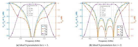
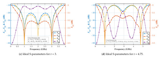
Figure 4.
Ideal S-parameters with variation of the frequency ratio.

Table 1.
Realizable frequency ratio.
4. The Prototype and Measurement Results
The proposed analytical design methodology is used to calculate the design parameters of a three-section WPD with 1 GHz, GHz, dB, and dB as an example. The calculated ideal design parameters using MATLAB are found to be as follows: . Subsequently, these values are used to implement and optimize the WPD in microstrip technology using a Cadence AWR design environment. All these values are optimized to balance the effects of junction discontinuity and component parasitics. The optimized design parameters are listed in Figure 5. The Roger’s RO4003C substrate parameters are as follows: , substrate height = 1.524 mm, and copper cladding = 1 oz/1 oz. The fabricated prototype is depicted in Figure 5a, whereas the measurement setup is shown in Figure 5b.
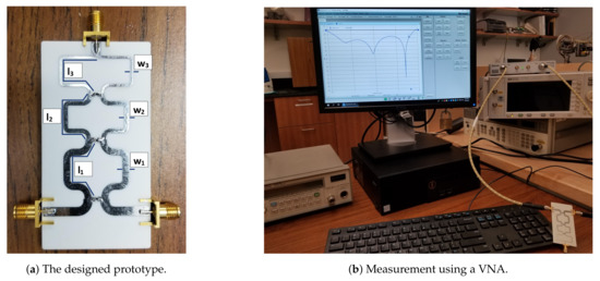
Figure 5.
The designed prototype using the proposed analytical design methodology and its measurement using a Tektronix TT506A VNA. The VNA display on the computer screen shows the measured isolation. Dimension (mm): l3 = 35, w3 = 1, l2 = 31.3, w2 = 1.65, l1 = 31.83, w1 = 2.54. Resistors (Ω) optimized to the closest commercially available values: 2R3 = 499, 2R2 = 232, 2R1 = 118.
The prototype is measured using a Tektronix TTR506A vector network analyzer (VNA) with a full two-port SOLT calibration. The electromagnetic simulation (EM) and the measured results in the range of 0.5–2.5 GHz are compared in Figure 6 and Figure 7.
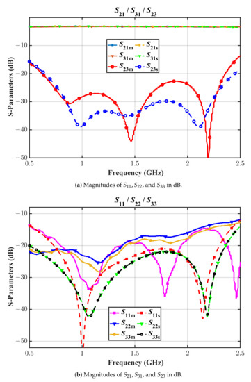
Figure 6.
The simulated and the measured s-parameters in dBs. Sijm stands for measured data and Sijs stands for simulated data.
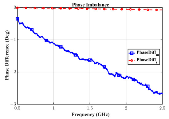
Figure 7.
The simulated and measured phase difference in degrees.
It is apparent from Figure 6a,b that the designed prototype has excellent transmission parameters maintaining an insertion-loss of lesser than dB (not very far from the ideal 3 dB value) throughout the band from 0.635 GHz to 2 GHz. A clear frequency shift is evident for the return-loss parameter , and its value is still better than 16 dB in the band from 0.635 GHz to 2 GHz, thanks to the over-design guaranteed by the proposed technique. There is some mismatch between the simulated and measured EM values which normally occur in any high-frequency design. In our case, it was possibly due to the Panasonic isolation resistor non-idealities at high frequencies. Unfortunately, the model of these resistors is not available, so it is not possible to include their impact in the simulation. Another potential reason for the mismatch can be the fabrication errors originating from limited milling accuracy. Nevertheless, the measured results show an outstanding performance of the proposed WPD, as it meets all the goals that a practical WPD will be required to meet during their deployment in the field, and we therefore accepted this result. Specifically, the measured isolation is excellent throughout the band with a minimum value of 22.7 dB. The measured phase imbalance is decent, remaining within 3 degrees, as shown in Figure 7.
Although the main advantage of the proposed design is its novel, fully analytical, and computer-friendly design methodology, to highlight the novelty of this work further, a comparison table is presented in Table 2. From this table, the %FBW enhancement is also discernible as compared to other previous notable works.
Table 2.
Comparison of the proposed design methodology and previous works.
5. Conclusions
A completely new analytical design methodology for a three-section WPD was presented in this paper. The methodology mixed the rigorous design equations with a dual-band design technique to arrive at a robust design that is more immune to process/component variations. The design methodology has been validated through several examples which dictate the capabilities of the proposed technique. Even though there was a slight mismatch between the simulated and measured results, they are still in good harmony, as all the design goals have been achieved with the fabricated prototype. In particular, the demonstration of a 104% fractional bandwidth ensuring a maximum 3.35 dB insertion loss and a minimum 16 dB of return loss and isolation is remarkable compared to other state-of-the-art techniques. Therefore, this novel approach has excellent potential to serve as a starting point for designing any ultra-wideband WPD in a very simple yet compact structure.
Author Contributions
Conceptualization, M.A.M.; methodology, M.A.M. and A.I.O.; software, M.A.M., A.I.O. and R.I.; validation, M.A.M., A.I.O. and R.I.; formal analysis, H.A.-S., A.N.S., Z.N.Z. and A.I.O.; investigation, M.A.M., A.I.O. and R.I.; resources, M.A.M., C.Z. and P.S.; data curation, A.I.O.; writing—original draft preparation, M.A.M. and A.I.O.; writing—review and editing, C.Z. and P.S.; visualization, A.I.O.; supervision, M.A.M. and C.Z. All authors have read and agreed to the published version of the manuscript.
Funding
This research received no external funding.
Institutional Review Board Statement
Not applicable.
Informed Consent Statement
Not applicable.
Data Availability Statement
Not applicable.
Acknowledgments
Mohammad Maktoomi and Christine Zakzewski would like to acknowledge the support from the Dean of the College of Arts and Sciences, Michelle Maldonado, the department of Physics and Engineering chairperson, W. Andrew Berger; Cadence for their AWRDE tool; and Rogers Corp. for the laminate samples.
Conflicts of Interest
The authors declare no conflict of interest.
References
- Wu, H.; Sun, S.; Wu, Y.; Liu, Y. Dual-band Gysel power dividers with large frequency ratio and unequal power division. Int. J. RF Microw. Comput. Aided Eng. 2020, 30, e22203. [Google Scholar] [CrossRef]
- Tas, V.; Atalar, A. An optimized isolation network for the Wilkinson divider. IEEE Trans. Microw. Theory Tech. 2014, 62, 3393–3402. [Google Scholar] [CrossRef]
- Cohn, S.B. A class of broadband three-port TEM-mode hybrids. IEEE Trans. Microw. Theory Tech. 1968, 16, 110–116. [Google Scholar] [CrossRef]
- Salman, M.; Jang, Y.; Lim, J.; Ahn, D.; Han, S.-M. Design of miniaturized Wilkinson power divider with higher order harmonic suppression for GSM application. Appl. Sci. 2021, 11, 4148. [Google Scholar] [CrossRef]
- Mohamed, E.N.; Sobih, A.G.; El-Tager, A.M.E. A novel compact size Wilkinson power divider with two transmission zeros for enhanced harmonics suppression. Prog. Electromag. Res. C 2018, 82, 67–76. [Google Scholar] [CrossRef][Green Version]
- Wang, X.; Sakagami, I.; Takahashi, K.; Okamura, S. A generalized dual-band Wilkinson power divider with parallel L,C, and R components. IEEE Trans. Microw. Theory Tech. 2012, 60, 952–964. [Google Scholar] [CrossRef]
- Maktoomi, M.A.; Akbarpour, M.; Hashmi, M.S.; Ghannouchi, F.M. On the dual-frequency impedance/admittance characteristic of multi-section commensurate transmission-line. IEEE Trans. Circuits Syst. II Exp. Briefs 2012, 64, 665–669. [Google Scholar] [CrossRef]
- Pozar, D.M. Microwave Engineering, 4th ed.; John Wiley and Sons, Inc.: Hoboken, NJ, USA, 2012. [Google Scholar]
- Gao, S.S.; Sun, S.; Xiao, S.Q. A novel wideband bandpass power divider with harmonic suppressed ring resonator. IEEE Microw. Wirel. Compon. Lett. 2013, 23, 119–121. [Google Scholar] [CrossRef]
- Ahn, H.-R.; Nam, S. 3-dB power dividers with equal complex termination impedances and design methods for controlling isolation circuits. IEEE Trans. Microw. Theory Tech. 2013, 61, 3872–3883. [Google Scholar] [CrossRef]
- Jiao, L.; Wu, Y.; Liu, Y.; Xue, Q.; Ghassemlooy, Z. Wideband filtering power divider with embedded transversal signal-interference sections. IEEE Microw. Wirel. Compon. Lett. 2017, 27, 1068–1070. [Google Scholar] [CrossRef]
- Chen, M.-T.; Tang, C.-W. Design of the filtering power divider with a wide passband and stopband. IEEE Microw. Wirel. Compon. Lett. 2018, 28, 570–572. [Google Scholar] [CrossRef]
- Liu, Y.; Zhu, L.; Sun, S. Proposal and design of a power divider with wideband power division and port-to-port isolation: A new topology. IEEE Trans. Microw. Theory Tech. 2020, 68, 1431–1438. [Google Scholar] [CrossRef]
Publisher’s Note: MDPI stays neutral with regard to jurisdictional claims in published maps and institutional affiliations. |
© 2021 by the authors. Licensee MDPI, Basel, Switzerland. This article is an open access article distributed under the terms and conditions of the Creative Commons Attribution (CC BY) license (https://creativecommons.org/licenses/by/4.0/).