Article

Linear Characterization and Modeling of GaN-on-Si HEMT Technologies with 100 nm and 60 nm Gate Lengths

1
Electronics Engineering, University of Roma Tor Vergata, Via del Politecnico 1, 00133 Roma, Italy
2
OMMIC SAS, 2 rue du Moulin, 94453 Limeil Brévannes, France
*
Author to whom correspondence should be addressed.
Electronics 2021, 10(2), 134; https://doi.org/10.3390/electronics10020134
Submission received: 27 November 2020 / Revised: 4 January 2021 / Accepted: 6 January 2021 / Published: 9 January 2021

Abstract

:
Motivated by the growing interest towards low-cost, restriction-free MMIC processes suitable for multi-function, possibly space-qualified applications, this contribution reports the extraction of reliable linear models for two advanced GaN-on-Si HEMT technologies, namely OMMIC’s D01GH (100 nm gate length) and D006GH (60 nm gate length). This objective is pursued by means of both classical and more novel approaches. In particular, the latter include a nondestructive method for determining the extrinsic resistances and an optimizaion-based approach to extracting the remaining parasitic elements: these support standard DC and RF measurements in order to obtain a scalable, bias-dependent equivalent-circuit model capturing the small-signal behavior of the two processes. As to the noise model, this is extracted by applying the well known noise-temperature approach to noise figure measurements performed in two different frequency ranges: a lower band, where a standard Y-factor test bench is used, and an upper band, where a custom cold-source test bench is set up and described in great detail. At 5 V drain-source voltage, minimum noise figures as low as 1.5 dB and 1.1 dB at 40 GHz have been extracted for the considered 100 nm and 60 nm HEMTs, respectively: this testifies the maturity of both processes and the effectiveness of the gate length reduction. The characterization and modeling campaign, here presented for the first time, has been repeatedly validated by published designs, a couple of which are reviewed for the Reader’s convenience.

1. Introduction

AlGaN/GaN heterostructure transistors are currently regarded as the natural successors to AlGaAs/GaAs HEMTs for microwave and millimeter-wave MMICs oriented to high-power or high-ruggedness applications. Among the several possible substrates [1], SiC is currently the most widely adopted trade-off between high thermal conductivity and low fabrication cost. Although historically driven towards high-power designs, the research on GaN HEMT technology has made significant progress as far as low-noise amplifiers are concerned [2,3,4]. At present, several GaN-based processes exist which not only outperform their GaAs counterparts in terms of output power but are even competitive in terms of noise factor, while inherently exhibiting superior ruggedness [5,6]. Such processes allow the integration of multiple functions on the same chip, which has naturally resulted in the concept of ‘single-chip front ends,’ that is, MMICs capable of performing high-power amplification in Tx-mode, low-noise amplification in Rx-mode, as well as switching between the two modes. A number of demonstrations on different European technologies have already been reported both in S-band [7,8,9] and C-band [10,11,12].
With the aim of further reducing the production costs and of securing substrate procurement from possible trade restrictions, foundries such as OMMIC have made significant efforts to replace SiC with Si, the latter being much cheaper and freely available on the market [13]. The obvious drawback of adopting Si over SiC comes from its lower thermal conductivity (1.5 W/cm/K vs. at least 3.0 W/cm/K, respectively), which at any rate is three times better than GaAs (0.5 W/cm/K). However, this limitation can be tolerated for applications in the millimeter-wave range (>30 GHz), where the available power densities are comparatively low. Also, Si substrates are very attractive due to the prospective integration capability with CMOS technologies [14,15]. Thus, GaN-on-Si processes have gained traction and definitely represent a major direction of research [16,17].
In this light, Europe has been funding research project on GaN technologies for at least a decade [18,19], as well as a recent project specifically oriented to millimeter-wave applications through GaN-on-Si technologies, named MiGaNSOS (Millimeter wave Gallium Nitride Space evaluation and application to Observation Satellites) [20]. Among the project’s objectives, the first consists in assessing and space-evaluating a state-of-the-art GaN-on-Si process for open foundry use, namely the 100 nm gate length GaN-on-Si technology developed by OMMIC (commercial name D01GH); at the same time, a preliminary assessment of its 60 nm evolution (D006GH) has been planned. In fact, the second goal is to demonstrate the simultaneous use of both 100 nm and 60 nm active devices on the same wafer and, actually, within the very same circuit, thus opening up a whole new range of possibilities in terms of design flexibility. Third, the projects aims at demonstrating future applications of the developed technologies in advanced space equipment. At circuit level, this translated into the design of fully integrated single-chip front ends operating in Ka-band [21].
This contribution aims to show the maturity of the two monolithic technologies from OMMIC for high-frequency, low-noise applications while providing a comprehensive description of the relevant characterization and modeling activities, which are not always standard. In particular, Section 3.2 reports both standard and more recent approaches to extract a bias-dependent, scalable small-signal equivalent-circuit (SSEC) model of the considered HEMTs. Also, the noise characterization of the active devices illustrated in Section 3.3 includes an in-depth description of a custom noise test bench operating in V-band which has been devised and set up specifically for this measurement campaign. The noise models yield interesting performance up to at least Ka-band and, as expected, show improved noise figure and gain for the reduced gate-length (i.e., 60 nm) option.
The article is organized as follows. Section 2 provides a general description of the two monolithic technologies from OMMIC. The characterization and modeling activities performed in the framework of the MiGaNSOS project are described in detail in Section 3. As a demonstration of the technology and of the models extracted, Section 4 overviews two MMICs operating at millimeter-waves which have been described in greater detail elsewhere [22,23,24]. The more novel ideas and methods of the characterization and modeling activities are discussed in Section 5, which also sketches the direction for further improving the V-band cold-source test bench. The main conclusions are then summarized in the final Section.

2. Technology

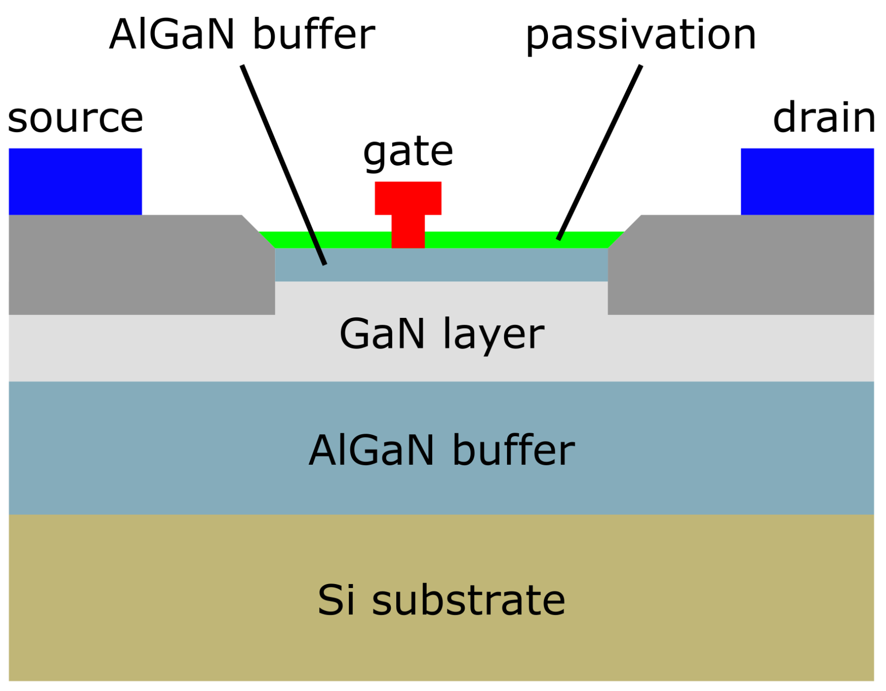
The GaN process developed by OMMIC and considered in the present study has been optimized for microwave and millimeter wave applications, including high-power amplification, robust low-noise amplification and switching functions. As schematically depicted in Figure 1, it consists in a GaN/AlGaN heterostructure grown on a high resistivity (5 kΩ/cm), 100 µm thick Silicon substrate. This process has the peculiarity of being available in two different gate length options, namely 100 nm and 60 nm, which go by the commercial names of D01GH and D006GH, respectively. The asymmetrical positioning of the gate contact and its peculiar mushroom shape has been optimized to raise the cutoff frequency of the devices, thus lowering any access parasitic resistance, and ensuring high gate-drain breakdown voltages.
Table 1 shows a brief comparison of the main performance of the D01GH and the D006GH technologies, as taken from OMMIC’s website [25]. As expected, the 60 nm option shows higher cutoff frequency and transconductance and a lower minimum noise figure with respect to the 100 nm option. They both show a very high breakdown voltage and a remarkable performance in terms of output RF power density.
Obviously, the same passive components are available in both options. These include two MIM capacitors, namely with capacitance densities of 400 pF/mm2 (SiN) and 50 pF/mm2 (SiN-SiO2); high and low precision resistors, namely with sheet resistances of 40 Ω/□ (NiCr) and 400 Ω/□ (GaN); square inductors; transmission lines; via holes. A comprehensive PDK allows easy placement, sizing and simulation of the components.
The D01GH and D006GH processes are available for open foundry runs. Also, the former is currently under space-grade qualification. It is noteworthy that the possibility of simultaneously using 60 nm and 100 nm active devices has also been explored, aiming at exploiting the peculiar benefits of both options for different purposes within the same circuit: see Section 4 for an example.

3. Results

This Section is split into three parts, following the subsequent logical steps conducive to a scalable, bias-dependent SSEC model. The first subsection deals with the preliminary screening and DC characterization. Then, the peculiarities of the small-signal measurements and of the SSEC model extraction are presented. Finally, the noise characterization and modeling are detailed.
While classical approaches represent a large share of the work, some relatively recent or new methods deserve being highlighted. In Section 3.2, the extrinsic resistances of the SSEC are obtained through a nondestructive extraction approach presented only lately, whereas the other extrinsic elements are obtained by a non-standard optimization-based approach with embedded scaling rules. Also, the cold-source test bench used for the V-band noise characterization has been purposely developed for this measurement campaign and is presented for the first time in Section 3.3. The level of detail of the description is such that the test bench can be precisely replicated.
The final models evidence the maturity of both processes and the tangible improvement resulting from the reduced 60 nm gate length. N F m i n values down to 1.5 dB and 1.1 dB were extracted for the D01GH and D006GH processes, respectively, at f = 40 GHz, V D S = 5 V.

3.1. Device Screening

The characterization campaign involved several device families in both the D01GH and D006GH processes, identified by the finger number N = 2 , 4 , 6 , 8 . Each device family comprises five geometries, with unit gate width W u = 13 , 35 , 50 , 70 , 100 µm. Thus, each geometry is identified by a self-explanatory label, such as 4x050. The main bulk of measurements and characterizations were performed on the 4x family, since the target functionality was represented by low-noise amplification. Several wafers were received from OMMIC and screened for representative devices.
While prolonged operation of the GaN transistors eventually stabilizes their behavior, the process is accelerated by a specific burn-in procedure for the sake of screening and subsequent characterization. In particular, before using the devices for the first time, they should be pinched off at a gate-source voltage V G S = 3 V while the drain-source voltage V D S is stepped from 0 V to 13 V, each step being maintained for 1 s; a last step at V D S = 15 V follows, which is maintained for 15 s, then V D S is stepped back, 1 V per second, to the desired value for actual operation; finally, V G S is also set to the required value. Threshold voltage and drain current densities were then measured for statistical and screening purposes.
Regarding the D01GH process, a threshold voltage V T H = 1.80 ± 0.26 V was determined, having defined V T H as the V G S voltage yielding a 10 mA/mm drain current density with V D S = 4 V. A similar value was obtained for the D006GH process, namely 1.84 ± 0.08 V. A reference bias point was also selected such that the corresponding drain current density is about half the expected maximum value: devices with drain current densities J D significantly away from the resulting reference value ( 511.1 ± 46.1 mA/mm and 609.0 ± 33.6 mA/mm, respectively) were excluded from further measurements.
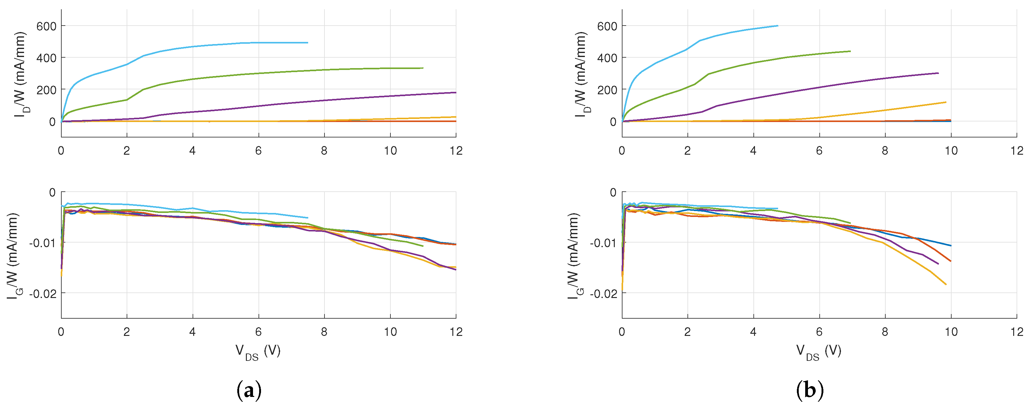
DC measurements were then carried out, with appropriate safety thresholds on maximum densities of drain current and power. V D S was swept from 0 V to 10 V while V G S was increased from −2 V to −0.75 V in 0.25 V steps. Additional measurements were taken for the D01GH process up to V D S = 12 V. As an example of DC measurements, see Figure 2.

3.2. Small-Signal Characterization and Modeling

The active devices here considered present a microstrip-oriented layout, with via holes connected to the source terminals. The advantages of this solution, as compared to a coplanar layout, are a minimal number of via holes (which however end up making part of the DUT itself) and a surer mono-modality. As to the calibration type, it is known that TRL [26] is sensitive to substrate loss if complemented with the typical capacitance method [27] instead of the more advanced calibration comparison method [28,29,30]. The latter, however, requires an auxiliary tier on a wafer-to-wafer basis. Thus, to simplify the calibration step, a commercial LRRM [31] algorithm was used. In all considered geometries, the DUT access lines were set equal to the half thru standard, so as to avoid any shifts of the reference planes and the consequent inaccuracies.
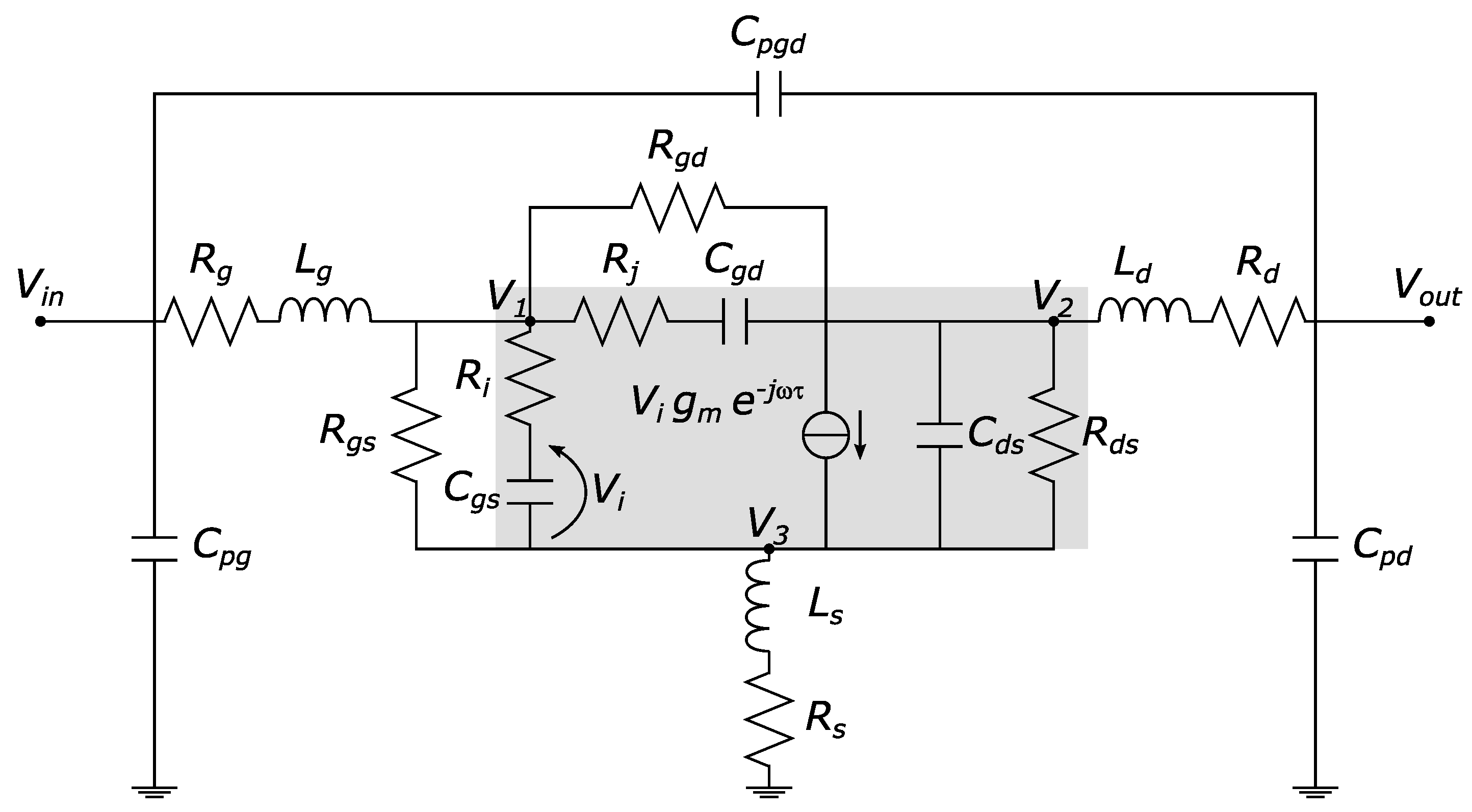
The operating point selected for the small-signal measurements belong to different groups, each targeted to address the extraction of a specific portion of the SSEC model (which is depicted in Figure 3):
  • cold-FET measurements: V D S = 0 V, swept V G S from below threshold to mild direct current;
  • hot-FET measurements over the V D S J D plane (same J D for multiple geometries);
  • hot-FET measurements over the V D S V G S plane.
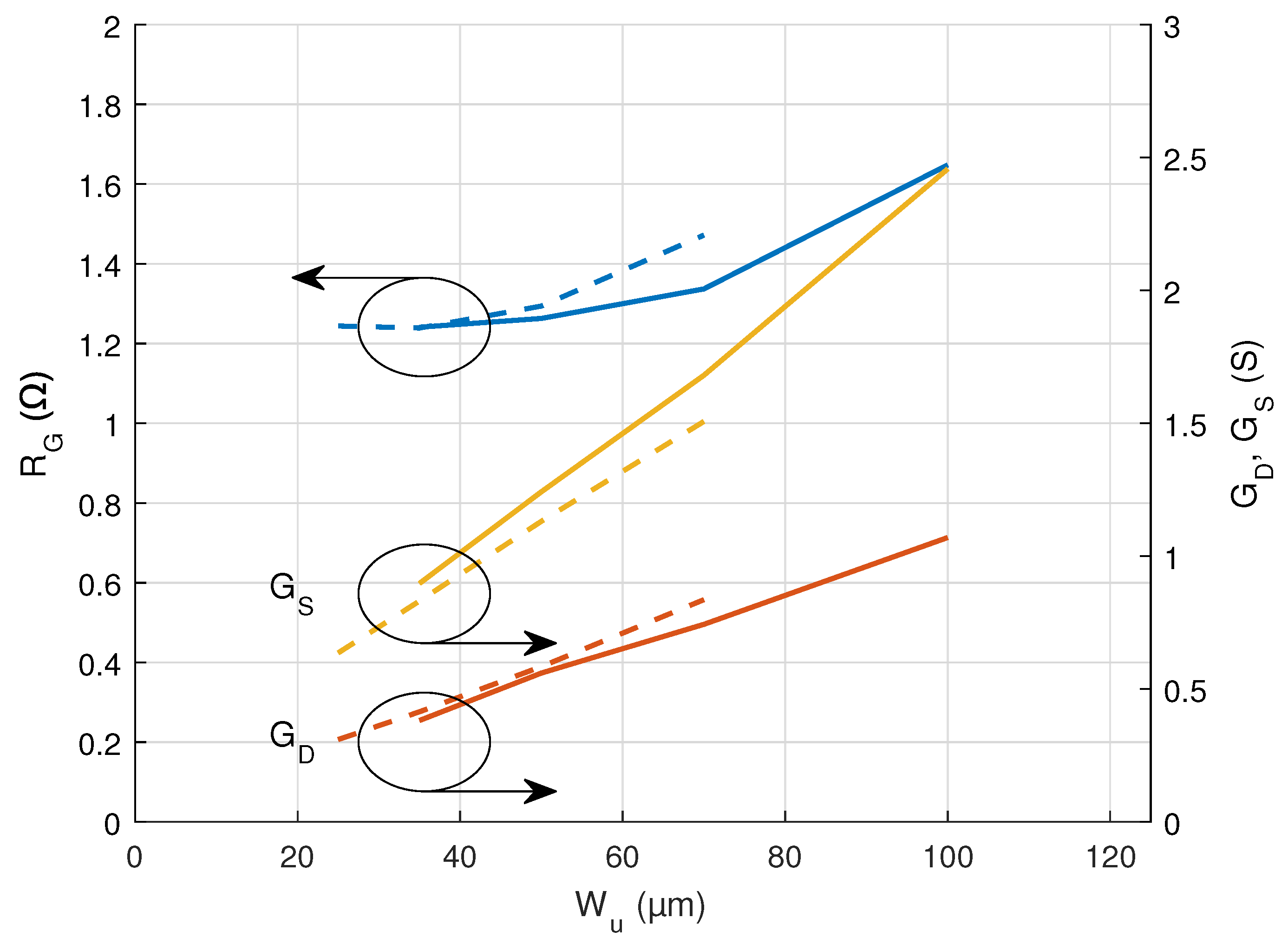
First, cold-FET measurements allowed the extraction of the parasitic resistances through a method recently described in Reference [32] without requiring significant DC gate currents: this prevents the DUTs from being excessively stressed during the small-signal characterization, so that the very same samples can be later characterized with respect to noise. Also, medium-frequency (5–20 GHz) measurements in mild direct current (open channel) allow estimating the source and drain inductances of each FET. The core idea of the method consists in identifying parameters of the gate-source junction when the device is operated at different cold (i.e., V D S = 0 V) bias points in mild forward condition. The identification is performed on the Z 11 parameters by means of pseudo-inversions. Then, the gate junction is subtracted from the Z-matrices, so that the only remaining bias dependency is that of the active channel. By identifying this dependency on V G S through another pseudo-inversion, the channel can be removed too and the sought-for extrinsic resistances are obtained. Figure 4 shows the result of this extraction on the two considered device families.
Subsequently, thanks to the constant- J D measurements, it is possible to meaningfully compare devices of different unit gate lengths W u across the same family. This is required from the method adopted for extracting the remaining extrinsic elements [33], which heavily exploits scaling rules. The previously determined elements were fixed as given functions of periphery, rather than being freely optimized. Pinch-off and open-channel measurements were also provided to the optimizer so as to fit the model to a variety of operation points. The actual optimization consists in minimizing a cost function c summing several errors ϵ , which in turn depend on unit gate width W u and bias point B. These errors sum over the i j S-parameters at different bias points, peripheries and frequencies and increase when the model deviates from measurements. For generality, they also include a weight varying with frequency and periphery. More specifically, the adopted formulae are as follows:
c = W u , B ϵ W u , B
ϵ W u , B = i , j , f w i , j f , W u · | S i , j m o d f , W u , B S i , j m e a s f , W u , B | 2 .
As a practical measure, the polynomials implementing the scaling rules do not depend directly on W u but on the ratio r = W u / W u , 0 , W u , 0 being the reference value of W u , so that the coefficients are better interpreted by the operator.
Finally, once the extrinsic model had been determined, a reference geometry (specifically, the 4x050) was subjected to a full extraction of the intrinsic circuit over the V D S V G S , in addition to the available operating points at constant J D . To this goal, standard closed formulae (see for example References [34,35]) were exploited in combination with linear fitting over appropriate frequency ranges, after mathematically removing the contribution of the extrinsic circuit. The general steps are as follows:
  • convert calibrated S-matrix to Y-matrix and subtract C p g , C p g d and C p d ;
  • convert resulting Y-matrix to Z-matrix and subtract R g , L g , R s , L s , R d and L d ;
  • convert resulting Z-matrix to Y-matrix and identify the intrinsic elements.
The last step is based on recognizing that the elements of the intrinsic Y-matrix have the following form:
Y i n t r = y g s + y g d y g d y g d + k i g m e j ω τ y d s + y g d
y g s = j ω C g s 1 + j ω C g s R i + G g s
y g d = j ω C g d 1 + j ω C g d R j + G g d
y d s = j ω C d s + G d s
k i = 1 1 + j ω C g s R i .
From the real and imaginary parts of y d s , respectively, G d s and C d s are trivially obtained as a constant and as a slope versus the angular frequency ω = 2 π f . G g s and G g d are the low-frequency limits of the real parts of y g s and y g d , respectively: after extracting them, one can compute 1 / y g s G g s and 1 / y g d G g d , which are of the general form:
1 y g x G g x = 1 + j ω C g x R x j ω C g x = R x + 1 j ω C g x .
The R x are directly extracted as constants versus frequency, while the C g x are the slopes of M M 1 / y g x G g x R x 1 versus ω . Having extracted R i and C g s , the coefficient k i can now be computed, so that from y 21 i n t r one obtains:
y 21 i n t r y 12 i n t r k i = g m e j ω τ ,
from which g m and τ follow:
g m = | y 21 i n t r y 12 i n t r k i |
τ = 1 ω · y 21 i n t r y 12 i n t r k i .
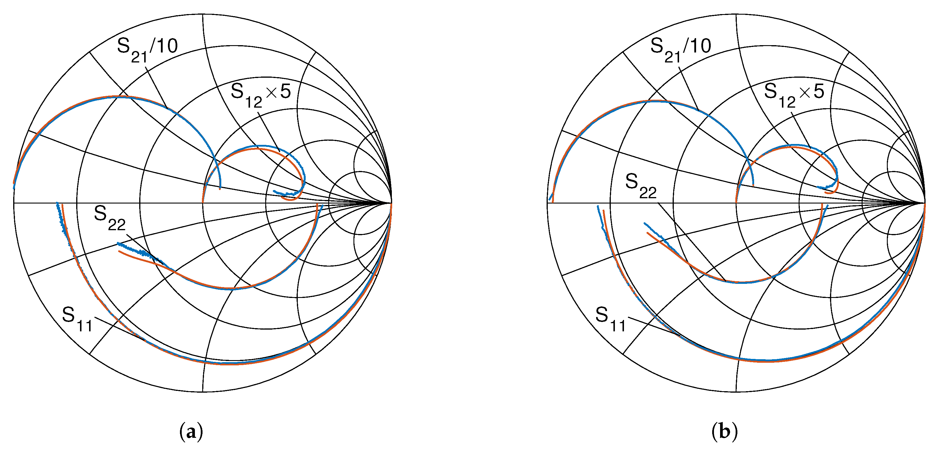
To give an idea of the final accuracy, a comparison of the modeled and measured S-parameters at a representative operating point is shown in Figure 5, for both the D01GH and D006GH technologies. The values of the SSEC components for the given operating points are reported in Table 2. The total circuit also includes EM -simulated via holes, to be added in series to the source terminal.
The intrinsic circuit of the reference device was finally applied to the other geometries by keeping the same time delay ( τ ) and scaling the other elements in the admittance representation, as usual (i.e., proportionally to W / W r e f ).

3.3. Noise Characterization and Modeling
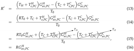
The noise characterization of the active devices was mainly based on a classic Y-factor test bench [36] working in the 10–20 GHz frequency band. The adopted solid-state noise source is characterized after a 10 dB attenuator, which yields a stable impedance when switching from cold to hot state. Further impedance stability comes from the unavoidable loss of the passive component chain between the noise source and the DUT, namely, the input bias-T and RF probe. The measured reflectance of the noise source in the hot state is allowed to compute the available gain of the input chain, which in turn was used to shift the noise source’s ENR to the DUT’s input reference plane as accurately as possible. In particular, one finds that:
R = T H T C T 0
Electronics 10 00134 i001
where R and R denote the ENR at the noise source and DUT sections; T C and T H are the cold and hot noise temperatures of the noise source; T e , P C C and T e , P C H represent the equivalent noise temperature of the passive chain when the noise source is in cold and hot state while G a v , P C C and G a v , P C H , similarly, denote its available gain in the same conditions; T 0 = 290 K is the standard temperature; T A is the ambient temperature. Finally, it has been assumed that T C = T A , so that:
T C + T e , P C X G a v , P C X = T A + 1 G a v , P C X 1 T A G a v , P C X ,
= T A
where X is a placeholder for C or H, indifferently.
As to the S-parameters of the input chain these were measured together with those of the output block (RF probe, bias-T) by a calibration comparison. Specifically, the outer tier was a coaxial SOLT calibration while the inner tier was an on-wafer LRRM. The output chain was then completed by a ferrite isolator, whose S-parameters were measured by a separate coaxial calibration.
In addition to the Y-factor test bench, a cold-source [36] test bench working in V-band was also set up, more specifically in the 50–75 GHz (WR-15) frequency range. The block diagram of the test bench is depicted in Figure 6, whereas overall and zoomed pictures are shown in Figure 7. The most noteworthy components are listed in the following:
  • an ELVA-1 ISSN-15 V-band noise source;
  • a SAGE Millimeter SFB-15-E2 V-band balanced mixer with external bias;
  • a SAGE Millimeter SWF-75379340-15-L1 V-band waveguide low-pass filter;
  • a SAGE Millimeter SWJ-15-TS V-band motorized waveguide switch;
  • a Low Noise Factory LNF-LNR45_77WA LNA;
  • a VDI WR15x3 frequency tripler.
As the receiver, an Agilent Power Spectrum Analyzer was used. The latter was tuned to different frequencies as the noise measurement frequency was swept, specifically selected to avoid significant spurious components from the tripler and mixer. Also, notice that the tuning capability of the spectrum analyzer was exploited to perform single-side band noise measurements, as required in order to extract a noise model.
The cold-source scheme was chosen for several reasons:
  • it allows a frequent calibration of the receiver while requiring only one solid-state noise source;
  • it simplifies the characterization of the input chain, which has to be known merely as a termination;
  • prospectively, it allows a simpler implementation of the source-pull technique.
The last point, however, has not actually been implemented in the current study. The source termination, on the contrary, was realized by the input port of an Anritsu VectorStar VNA for checking purposes, as will be explained shortly.
Indeed, cold-source measurements of the noise temperature at the input of the equivalent receiver are inherently accurate [36], especially when a frequent automatic calibration is performed and the relevant component chain is rigidly connected. However, it is critical to correctly shift that measurement to the output port of the DUT and, more importantly, to convert the latter output noise temperature T n , o u t , D U T into an equivalent noise temperature T e , D U T :
T e , D U T = T n , o u t , D U T G a v , D U T T n , S ,
where the symbols are self-explanatory. Notice that the source noise temperature equals the ambient temperature in this case (i.e., T n , S = T A ): to this purpose, the VNA input port must clearly be turned off when taking noise measurements. In addition to the noise measurements, the VNA input port is turned on at a reference power level and a power reading is taken. By comparing this reading to one with the DUT replaced by a thru standard, an insertion gain can be computed and compared to the expected available gain. See Section 5 for further details on this aspect.
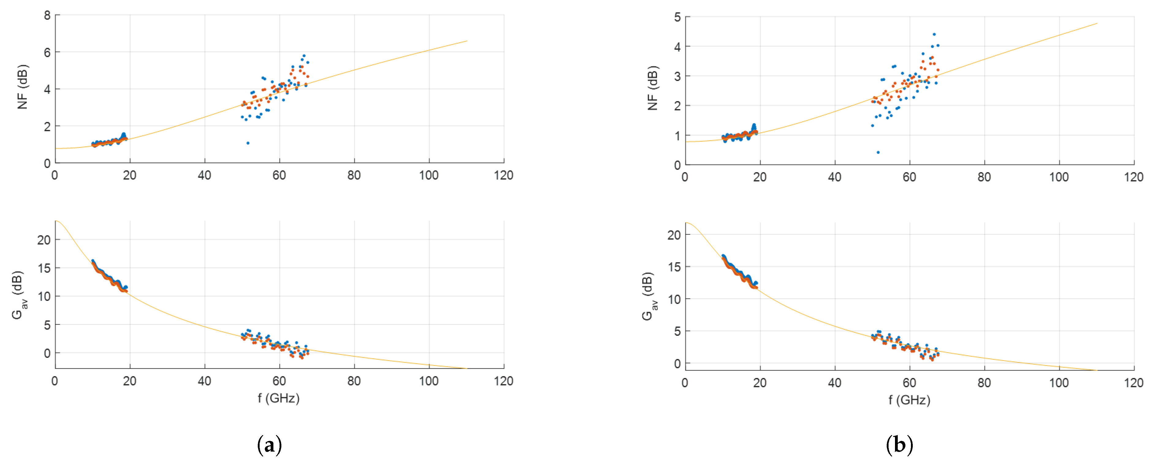
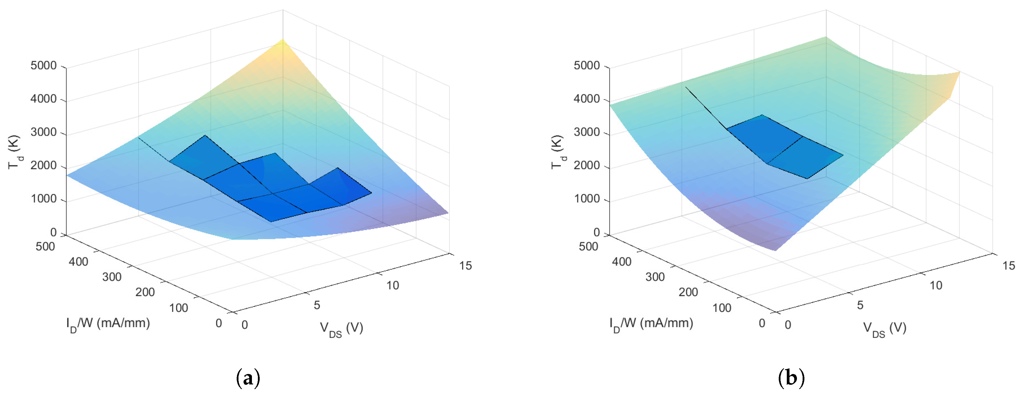
By combining noise measurements in the 10–20 GHz and 50–65 GHz frequency bands with the SSEC model of the active devices, the gate and drain noise temperatures T g and T d [37] were extracted by means of the algorithm described in References [33,38]. Figure 8 shows examples of these extractions (actually, what can be shown is the resulting fit of the model to the noise figure and associated gain). Repeating the process for multiple operating points across the V D S J D plane produces isolated points of the T g and T d surfaces, which can then fitted by a polynomial model: this yields results such as those shown in Figure 9, which assume a 6-term model of the form c 00 + c 10 V G S + c 01 J D + c 20 V G S 2 + c 11 V G S J D + c 02 J D 2 . As to J D , it also is polynomially fitted to a meaningful range of V G S and V D S , which are the input parameters of the equivalent model.
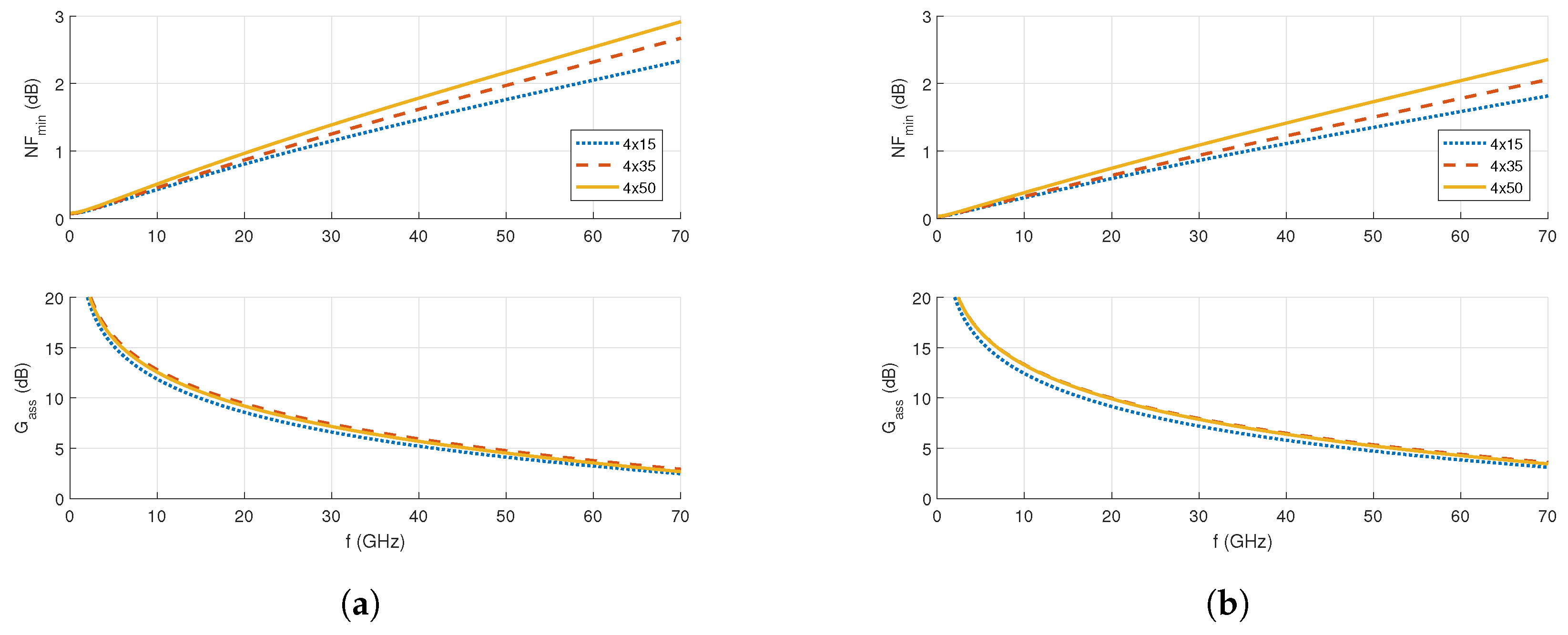
Figure 10 summarizes the main results of the modeling campaign from a noise-oriented standpoint. In particular, if the D01GH is considered, the minimum noise figure extracted for the reference geometry (i.e., 4x050) is approximately 1.8 dB at 40 GHz, with an associated gain (i.e., available gain at the same source termination) of about 5.7 dB. As to the D006GH, the minimum noise figure becomes 1.4 dB at the same frequency, whereas the associated gain increases to 6.4 dB. For both technologies, the drain-source voltage is 5 V and the gate-source voltage is tuned for best N F m i n ( V G S 1.25 V).
In addition to the operating point, the minimum noise figure is of course dependent on other factors, and primarily on device geometry. Figure 10 also shows that further improvements in N F m i n come from smaller unit gate widths. In the D01GH case, N F m i n reaches down to 1.5 dB when W u = 15 µm. Correspondingly, the value for the D006GH is 1.1 dB.

4. Test Vehicles

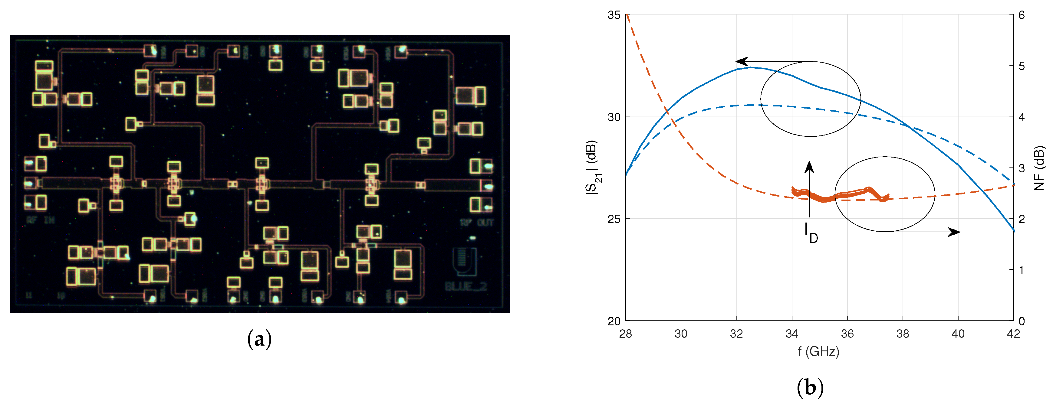
As a first test vehicle of the extracted small-signal and noise models, a Ka-band low-noise amplifier is briefly illustrated [22] which is an improved version of the PDK-based design presented in Reference [23]. The LNA adopts a 4-stage topology and covers the 35–37 GHz frequency range. The first two stages are designed to fulfill a noise/gain trade-off while the remaining two stages are synthesized to obtain the prescribed gain specification. In this way, a linear gain in excess of 30 dB is accomplished. The LNA’s noise figure is 2.3 dB. This performance is rather interesting considering the LNA has an input power survivability of at least +20 dBm. Measured results are in excellent agreement with simulations thanks to the accuracy of the proposed small signal and noise models of the active device. Figure 11 shows a microphoto of the LNA and the main performance indicators.
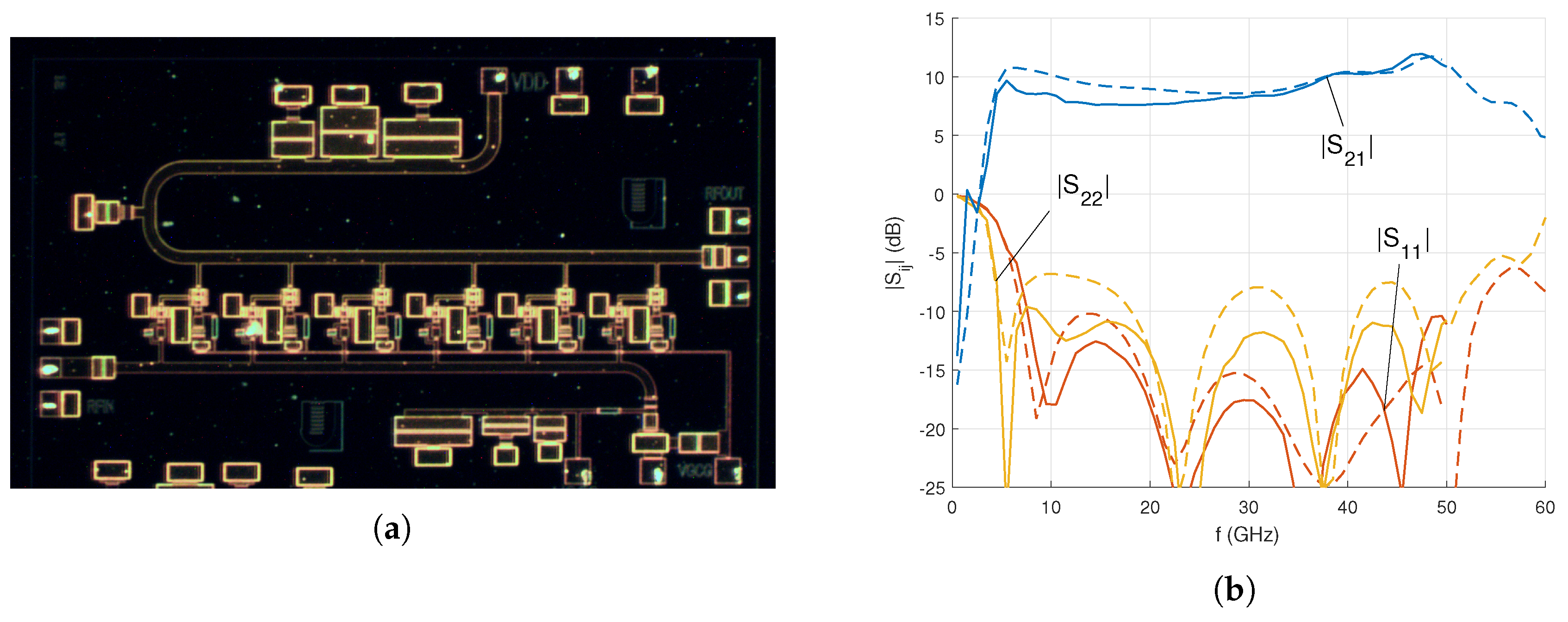
As a second demonstration, a realization is produced which simultaneously uses, within the very same MMIC, both the 100 nm and 60 gate-length options. This feature provides interesting possibilities for high-frequency designers, who get to be able to choose the better active device option for each specific function. In the present case, a travelling-wave amplifier is summarized [24] exploiting a cascode cell as the voltage-controlled current source: see Figure 12a for a picture. In turn, the cascode cell employs a 60 nm device as the common-source transistor and a 100 nm device as the common-gate transistor. Measurements confirm satisfactory operation in the 5–52 GHz frequency range, as reported in Figure 12b. This corresponds to a bandwidth improvement of about +20%, with respect to the simulated 100 nm-only solution.

5. Discussion and Future Research

Among the various adopted characterization and modeling techniques, as already observed, many are standard, but others have been presented only recently, and in particular: the extraction method for the extrinsic resistances [32], the optimization-based method used to determine the other extrinsic parameters [33], the custom V-band cold-source test bench. These techniques can be (and in some cases have been) applied not only to GaN-based HEMTs but to other technologies as well: thus, the material presented in this study finds a broad applicability in a variety of other contexts.
With regard to the cold-source test bench, which has been presented in this contribution for the first time, several developments are still ongoing. In particular, as already outlined, in order to perform accurate measurements it is critical that the available gain of the DUT be accurately determined, since it directly affects the extracted noise temperature through Equation (19). Although the DUT’s S-parameter are measured at a previous time with a different test bench, the operating point V D S J D is reproduced as accurately as possible thanks to an iterative algorithm, so as to ideally put the DUT in the very same working conditions. Nevertheless, possible fluctuations or drifts of the DUT gain may be due to instabilities of the technology, rather than to limitations of the test bench.
As a safeguard against such instabilities, a rough double check of the DUT gain during the noise measurement was carried out by exploiting the insertion gain between scalar power measurements: one on a thru standard, serving as the reference, and the other on the active devices in the appropriate operating points. The insertion gain can be corrected into an available gain through the knowledge of the DUT’s source reflection coefficient, the receiver’s input reflection coefficient, the S-parameters of the output passive block and the S 11 and S 22 parameters of the DUT. These last two can be assumed to be not very sensitive to the operating point.
However, the above approach is suboptimal with respect to measuring the whole DUT S-matrix concurrently with the noise measurement itself (i.e., without changing the operating point between the two steps). In principle, this would readily be allowed by the block diagram shown in Figure 6, albeit at V-band frequencies only: to that end, it would be sufficient to connect the VNA output port to the free connector of the DPDT switch. Unfortunately, such a possibility could not be exploited during the characterizations, mainly due to the unavailability of an adequate mechanical support allowing a reliable connection of the output port cable. As soon as such a mechanical support is procured, the results obtained with the present test bench should be compared to those yielded by the complete scheme.
The ultimate goal (i.e., after demonstrating the repeatability and accuracy of the approach) is for the cold-source measurements to do without the VNA entirely, so that the source termination can also be made different from a matched load and, thus, a source-pull algorithm safely implemented.

6. Conclusions

Within the general framework introductorily provided on the status and trends of research on GaN HEMT technologies, two advanced commercial processes (namely OMMIC’s D01GH and D006GH) have been presented. A complex characterization and modeling campaign has been presented in great detail, reporting both standard and novel methods which may come in handy to Readers dealing with other microwave and millimeter-wave technologies. The capabilities of the two processes and the validity of the extracted models have been demonstrated through measurements of realized MMICs. Notes on the more innovative approaches and on further developments have also been provided.

Author Contributions

Conceptualization, S.C. and W.C.; methodology, S.C. and W.C.; software, S.C.; validation, L.P. and P.E.L.; formal analysis, S.C.; resources, J.P. and R.L.; data curation, S.C. and W.C.; writing—original draft preparation, S.C.; writing—review and editing, P.E.L.; supervision, E.L.; project administration, E.L.; funding acquisition, E.L. All authors have read and agreed to the published version of the manuscript.

Funding

This research and the APC were funded by the European Union under project H2020-COMPET-2017 MiGANSOS, grant number 776322.

Data Availability Statement

The data are confidential between the project partners and therefore not publicly available.

Conflicts of Interest

The authors declare no conflict of interests. The funders had no role in the design of the study; in the collection, analyses, or interpretation of data; in the writing of the manuscript, or in the decision to publish the results.

Abbreviations

The following abbreviations are used in this manuscript:
AlGaNAluminium Gallium Nitride
GaNGallium Nitride
GaAsGallium Arsenide
SiSilicon
SiCSilicon Carbide
SiNSilicon Nitride
SiO2Silicon Dioxide
NiCrNickel Chromium
FETField-Effect Transistor
HEMTHigh Electron Mobility Transistor
DUTDevice Under Test
LNALow-Noise Amplifier
SCFESingle-Chip Front End
MMICMonolithic Microwave Integrated Circuit
DPDTDouble-Pole Double-Throw
SPDTSingle-Pole Double-Throw
TxTransmit (mode)
RxReceive (mode)
SSECSmall-Signal Equivalent Circuit
MIMMetal-Insulator-Metal
DCDirect Current
RFRadio Frequency
VNAVector Network Analyzer
TRLThru Reflect Line
LRRMLine Reflect Reflect Match
EMElectromagnetic
ENRExcess Noise Ratio

References

  1. Joshi, B.C.; Dhanavantri, C.; Kumar, D. Sapphire, SiC, AlN, Si and diamond-substrate material for GaN HEMT and LED. J. Optoelectron. Adv. Mater. 2009, 11, 1111–1116. [Google Scholar]
  2. Masuda, S.; Yamada, M.; Ohki, T.; Makiyama, K.; Okamoto, N.; Nakasha, Y.; Imanishi, K.; Kikkawa, T.; Shigematsu, H. C-Ku band GaN MMIC T/R frontend module using multilayer ceramics technology. In Proceedings of the IEEE MTT-S International Microwave Symposium, Baltimore, MD, USA, 5–10 June 2011; pp. 1–4. [Google Scholar] [CrossRef]
  3. Schuh, P.; Reber, R. Robust X-band low noise limiting amplifiers. In Proceedings of the IEEE MTT-S International Microwave Symposium Digest (MTT), Seattle, WA, USA, 2–7 June 2013; pp. 1–4. [Google Scholar] [CrossRef]
  4. Suijker, E.M.; Rodenburg, M.; Hoogland, J.A.; van Heijningen, M.; Seelmann-Eggebert, M.; Quay, R.; Bruckner, P.; van Vliet, F.E. Robust AlGaN/GaN Low Noise Amplifier MMICs for C-, Ku- and Ka-Band Space Applications. In Proceedings of the Annual IEEE Compound Semiconductor Integrated Circuit Symposium, Greensboro, NC, USA, 11–14 October 2009; pp. 1–4. [Google Scholar] [CrossRef] [Green Version]
  5. Rudolph, M. GaN HEMTs for low-noise amplification—Status and challenges. In Proceedings of the Integrated Nonlinear Microwave and Millimetre-wave Circuits Workshop (INMMiC), Graz, Austria, 20–21 April 2017; pp. 1–4. [Google Scholar] [CrossRef]
  6. Ciccognani, W.; Colangeli, S.; Serino, A.; Pace, L.; Fenu, S.; Longhi, P.E.; Poulain, J.; Leblanc, R. Comparative noise investigation of high-performance GaAs and GaN millimeter-wave monolithic technologies. In Proceedings of the European Microwave Integrated Circuits Conference (EuMIC), Paris, France, 30 September–1 October 2019; pp. 192–195. [Google Scholar]
  7. Giofrè, R.; Costanzo, F.; Ciccognani, W.; Colangeli, S.; Limiti, E. A GaN Single-Chip Front End With Improved Efficiency and Power by Using Class F Approach. IEEE Microw. Wirel. Compon. Lett. 2019, 29, 140–142. [Google Scholar] [CrossRef]
  8. Ciccognani, W.; Colangeli, S.; Costanzo, F.; Giofrè, R.; Polli, G.; Salvucci, A.; Vittori, M.; Limiti, E.; Sotgia, M.; Cirillo, M. A GaN Single-Chip Front-End for Active Electronically Scanned Arrays. In Proceedings of the IEEE/MTT-S International Microwave Symposium (IMS), Philadelphia, PA, USA, 10–15 June 2018; pp. 613–615. [Google Scholar] [CrossRef]
  9. Giofrè, R.; Colangeli, S.; Ciccognani, W.; Costanzo, F.; Polli, G.; Salvucci, A.; Vittori, M.; Sotgia, M.; Cirillo, M.; Limiti, E. S-Band GaN Single-Chip Front End for Active Electronically Scanned Array With 40-W Output Power and 1.75-dB Noise Figure. IEEE Trans. Microw. Theory Tech. 2018, 66, 5696–5707. [Google Scholar] [CrossRef]
  10. Giofrè, R.; Ciccognani, W.; Colangeli, S.; Feudale, M.; Lanzieri, C.; Polli, G.; Salvucci, A.; Suriani, A.; Vittori, M.; Limiti, E. A C-Band GaN Single Chip Front-End for SAR Applications. In Proceedings of the IEEE Radio and Wireless Symposium (RWS), San Antonio, TX, USA, 26–29 January 2020; pp. 162–164. [Google Scholar] [CrossRef]
  11. Salvucci, A.; Polli, G.; Vittori, M.; Giofrè, R.; Colangeli, S.; Ciccognani, W.; Limiti, E.; Carosi, D.; Feudale, M.; Lanzieri, C.; et al. A GaN single chip front-end for C-band synthetic aperture radars. In Proceedings of the International Microwave and Radar Conference (MIKON), Poznan, Poland, 14–17 May 2018; pp. 504–507. [Google Scholar] [CrossRef]
  12. van Heijningen, M.; de Hek, P.; Dourlens, C.; Fellon, P.; Adamiuk, G.; Ayllon, N.; van Vliet, F. C-Band Single-Chip Radar Front-End in AlGaN/GaN Technology. IEEE Trans. Microw. Theory Tech. 2017, 65, 4428–4437. [Google Scholar] [CrossRef]
  13. Limiti, E.; Colangeli, S.; Bentini, A.; Nanni, A. Characterization and modeling of low-cost, high-performance GaN-Si technology. In Proceedings of the International Conference on Microwaves, Radar and Wireless Communications (MIKON), Warsaw, Poland, 21–23 May 2012; Volume 2. [Google Scholar]
  14. Kazior, T.E.; LaRoche, J.R.; Ip, K.; Kennedy, T.; Knickerbocker, J.; Tsang, C.; Soirez, L. More Than Moore—Wafer Scale Integration of Dissimilar Materials on a Si Platform. In Proceedings of the IEEE Compound Semiconductor Integrated Circuit Symposium (CSICS), New Orleans, LA, USA, 11–14 October 2015; p. 1. [Google Scholar] [CrossRef]
  15. Kazior, T.E.; LaRoche, J.R.; Hoke, W.E. More Than Moore: GaN HEMTs and Si CMOS Get It Together. In Proceedings of the IEEE Compound Semiconductor Integrated Circuit Symposium (CSICS), Monterey, CA, USA, 13–16 October 2013; pp. 1–4. [Google Scholar] [CrossRef]
  16. Boles, T. GaN-on-silicon present challenges and future opportunities. In Proceedings of the European Microwave Integrated Circuits Conference (EuMIC), Nuremberg, Germany, 8–10 October 2017; pp. 21–24. [Google Scholar] [CrossRef]
  17. Hsu, S.S.H.; Tsou, C.; Lian, Y.; Lin, Y. GaN-on-silicon devices and technologies for RF and microwave applications. In Proceedings of the IEEE International Symposium on Radio-Frequency Integration Technology (RFIT), Taipei, Taiwan, 24–26 August 2016; pp. 1–3. [Google Scholar] [CrossRef]
  18. Buchta, M.; Beilenhoff, K.; Blanck, H.; Thorpe, J.; Behtash, R.; Heckmann, S.; Jung, H.; Ouarch, Z.; Camiade, M. GaN technologies and developments: Status and trends. In Proceedings of the International Conference on Microwave and Millimeter Wave Technology, Chengdu, China, 8–11 May 2010; pp. 488–491. [Google Scholar] [CrossRef]
  19. Reveyrand, T.; Ciccognani, W.; Ghione, G.; Jardel, O.; Limiti, E.; Serino, A.; Camarchia, V.; Cappelluti, F.; Quéré, R. GaN Transistor Characterisation and Modelling Activities Performed within the Frame of the KorriGaN Project. Int. J. Microw. Wirel. Technol. 2010, 2, 51–61. [Google Scholar] [CrossRef] [Green Version]
  20. CORDIS’ Website on the MiGaNSOS Project. Available online: https://cordis.europa.eu/project/id/776322/ (accessed on 6 January 2021).
  21. Pace, L.; Costanzo, F.; Longhi, P.; Ciccognani, W.; Colangeli, S.; Suriani, A.; Leblanc, R.; Limiti, E. Design of a Ka-band single-chip front-end based on a 100 nm GaN-on-Si technology. In Proceedings of the Integrated Nonlinear Microwave and Millimetre-Wave Circuits Workshop (INMMiC), Cardiff, UK, 16–17 July 2020. [Google Scholar] [CrossRef]
  22. Pace, L.; Colangeli, S.; Ciccognani, W.; Longhi, P.E.; Limiti, E.; Leblanc, R.; Feudale, M.; Vitobello, F. Design and validation of 100 nm GaN-on-Si Ka-Band LNA based on custom noise and small signal models. Electronics 2020, 9, 150. [Google Scholar] [CrossRef] [Green Version]
  23. Pace, L.; Ciccognani, W.; Colangeli, S.; Longhi, P.E.; Limiti, E.; Pace, L.; Ciccognani, W.; Colangeli, S.; Longhi, P.E.; Limiti, E.; et al. A Ka-band low-noise amplifier for space applications in a 100 nm GaN on Si technology. In Proceedings of the Conference on Ph.D Research in Microelectronics and Electronics (PRIME), Lausanne, Switzerland, 15–18 July 2019; pp. 161–164. [Google Scholar] [CrossRef]
  24. Longhi, P.; Colangeli, S.; Ciccognani, W.; Pace, L.; Leblanc, R.; Limiti, E. C to V-band cascode distributed amplifier design leveraging a double gate length Gallium Nitride on Silicon process. In Proceedings of the IEEE MTT-S International Microwave Symposium Digest, Los Angeles, CA, USA, 4–6 August 2020; pp. 409–412. [Google Scholar] [CrossRef]
  25. OMMIC’s Website. Available online: https://www.ommic.com/iii-v-processes/ (accessed on 6 January 2021).
  26. Engen, G.F.; Hoer, C.A. Thru-Reflect-Line: An Improved Technique for Calibrating the Dual Six-Port Automatic Network Analyzer. IEEE Trans. Microw. Theory Tech. 1979, 27, 987–993. [Google Scholar] [CrossRef] [Green Version]
  27. Williams, D.F.; Marks, R.B. Transmission line capacitance measurement. IEEE Microw. Guid. Wave Lett. 1991, 1, 243–245. [Google Scholar] [CrossRef]
  28. Williams, D.F.; Arz, U.; Grabinski, H. Characteristic-impedance measurement error on lossy substrates. IEEE Microw. Wirel. Compon. Lett. 2001, 11, 299–301. [Google Scholar] [CrossRef]
  29. Pulido-Gaytán, M.A.; de Landa, A.Z. Determination of the Line Characteristic Impedance Using Calibration Comparison. In Proceedings of the ARFTG Microwave Measurement Conference, Philadelphia, PA, USA, 15 June 2018; pp. 1–3. [Google Scholar] [CrossRef]
  30. Williams, D.F.; Marks, R.B.; Davidson, A. Comparison of On-Wafer Calibrations. In Proceedings of the ARFTG Conference Digest, San Diego, CA, USA, 5–6 December 1991; Volume 20, pp. 68–81. [Google Scholar] [CrossRef]
  31. Davidson, A.; Jones, K.; Strid, E. LRM and LRRM Calibrations with Automatic Determination of Load Inductance. In Proceedings of the ARFTG Conference Digest, Monterey, CA, USA, 29–30 November 1990; Volume 18, pp. 57–63. [Google Scholar] [CrossRef]
  32. Colangeli, S.; Ciccognani, W.; Serino, A.; Longhi, P.E.; Pace, L.; Poulain, J.; Leblanc, R.; Limiti, E. Nondestructive, Self-Contained Extraction Method of Parasitic Resistances in HEMT Devices. IEEE Trans. Microw. Theory Tech. 2020, 68, 2571–2578. [Google Scholar] [CrossRef]
  33. Colangeli, S.; Ciccognani, W.; Cleriti, R.; Palomba, M.; Limiti, E. Optimization-based approach for scalable small-signal and noise model extraction of GaN-on-SiC HEMTs. Int. J. Numer. Model. Electron. Netw. Devices Fields 2017, 30, e2135. [Google Scholar] [CrossRef]
  34. Dambrine, G.; Cappy, A.; Heliodore, F.; Playez, E. A new method for determining the FET small-signal equivalent circuit. IEEE Trans. Microw. Theory Tech. 1988, 36, 1151–1159. [Google Scholar] [CrossRef]
  35. Berroth, M.; Bosch, R. Broad-band determination of the FET small-signal equivalent circuit. IEEE Trans. Microw. Theory Tech. 1990, 38, 891–895. [Google Scholar] [CrossRef] [Green Version]
  36. Tiemeijer, L.F.; Havens, R.J.; de Kort, R.; Scholten, A.J. Improved Y-factor method for wide-band on-wafer noise-parameter measurements. IEEE Trans. Microw. Theory Tech. 2005, 53, 2917–2925. [Google Scholar] [CrossRef]
  37. Pospieszalski, M.W. Modeling of noise parameters of MESFETs and MODFETs and their frequency and temperature dependence. IEEE Trans. Microw. Theory Tech. 1989, 37, 1340–1350. [Google Scholar] [CrossRef]
  38. Mokari, M.E.; Patience, W. A new method of noise parameter calculation using direct matrix analysis. IEEE Trans. Circuits Syst. I Fundam. Theory Appl. 1992, 39, 767–771. [Google Scholar] [CrossRef]
Samples are to be requested to the foundry.
Figure 1. Simplified active layer profile of the D01GH and D006GH technologies.
Electronics 10 00134 g001
Figure 2. Normalized DC characteristics of 4x050 devices, as V G S is increased from −2 V to −0.75 V in 0.25 V steps: (a) D01GH (b) D006GH.
Electronics 10 00134 g002
Figure 3. Schematic of the adopted SSEC.
Electronics 10 00134 g003
Figure 4. Extracted resistive elements of the extrinsic circuit. Continuous lines: D01GH. Dashed lines: D006GH.
Electronics 10 00134 g004
Figure 5. S-parameters of 4x050 devices up to 50 GHz: (a) D01GH, V D S = 5 V, I D = 20.4 mA (b) D006GH, V D S = 5 V, I D = 24.4 mA.
Electronics 10 00134 g005
Figure 6. V-band cold-source noise test bench: block diagram. From the left to the right along the measurement chain: (cold) matched termination, input bias-T, input RF probe, DUT, output RF probe, output bias-T, DPDT switch, ferrite isolator, pre-amplifier, low-pass filter, mixer, receiver. The DPDT switch is in addition connected to a solid-state noise source. The LO port of the mixer is driven by the cascade of a signal source, an amplifier and a frequency tripler.
Electronics 10 00134 g006
Figure 7. V-band cold-source noise test bench: (a) Full view (b) Detail of the switch and down-conversion section.
Electronics 10 00134 g007
Figure 8. Noise figure and associated gain resulting from noise temperature extractions for 4x050 devices at V D S = 5 V. Points represent the measurement-fitting comparison on the actual source terminations seen by the DUT. Continuous lines represent the modeled values on standard terminations: (a) D01GH, I D = 61.2 mA. (b) D006GH, I D = 73.2 mA.
Electronics 10 00134 g008
Figure 9. Noise temperature extraction and fitting for 4x050 devices. The vertices of the opaque patches represent actual extraction points. The transparent surfaces represent the polynomial fittings: (a) D01GH. (b) D006GH.
Electronics 10 00134 g009
Figure 10. Minimum noise figure and associated gain extracted for 4x devices at V D S = 5 V, V G S 1.25 V: (a) D01GH. (b) D006GH.
Electronics 10 00134 g010
Figure 11. 4-stage LNA in the D01GH process: (a) Picture. (b) Performance. Continuous traces: measurements. Dashed traces: simulations. The nominal operating point is V D D = 5 V, I D = 150 mA. The variation of N F for drain currents from 109 mA to 182 mA is also shown.
Electronics 10 00134 g011
Figure 12. Distributed cascode amplifier with mixed 100 nm/60 nm option: (a) Picture. (b) Performance. Continuous traces: measurements. Dashed traces: simulations. The nominal operating point is V D D = 12 V, I D = 210 mA.
Electronics 10 00134 g012
Table 1. Main features of chosen GaN-on-Si technologies.
ParameterD01GHD006GH
Gate length100 nm60 nm
Cutoff frequency110 GHz150 GHz
Maximum oscillation frequency180 GHz190 GHz
Gate-drain breakdown voltage (1)36 V36 V
Maximum drain current density1200 mA/mm1200 mA/mm
Maximum extrinsic transconductance800 mS/mm950 mS/mm
Minimum noise figure at 40 GHz1.5 dB1.1 dB
RF power density4 W/mm (2)3.3 W/mm
(1) The reported value is the minimum guaranteed corresponding to 300 μA/mm current densities. (2) The actual value clearly depends on several conditions, starting with base plate temperature and heat dissipation capability. Values as high as 6 W/mm have been reached, but the recommended value is 3.3 W/mm.
Table 2. Sample values of SSEC elements at V D S = 5 V.
ParameterUnitD01GH ( I D = 20.4 mA)D006GH ( I D = 24.4 mA)
C p g F9.2306 × 10 15 9.7087 × 10 15
C p d F7.5285 × 10 15 5.1388 × 10 15
C p g d F8.2609 × 10 15 8.5547 × 10 15
τ s2.2607 × 10 13 3.7819 × 10 13
L g H2.4735 × 10 11 2.5441 × 10 11
L d H2.5520 × 10 11 2.5763 × 10 11
L s H1.5125 × 10 12 1.8542 × 10 12
R g 1.25371.2931
R d 1.84001.6700
R s 0.80000.8600
C g s F2.1598 × 10 13 1.7146 × 10 13
C d s F8.3262 × 10 14 7.8070 × 10 14
C g d F3.2511 × 10 14 3.4192 × 10 14
R i 3.07550.4741
R j 14.463215.9634
G g s S5.6334 × 10 5 0
G d s S0.00590.0084
G g d S8.6424 × 10 6 5.3925 × 10 6
g m S0.13220.1479
Publisher’s Note: MDPI stays neutral with regard to jurisdictional claims in published maps and institutional affiliations.