Abstract
An improved hybrid submodule employs a direct current (DC) short current protection function to improve the reliability of a high-voltage direct current (HVDC) system. However, it increases the number of circuit components to implement the protection. So, we need to evaluate the relationship between the protection function and the increased number of circuit components to assess whether the improved hybrid submodule (IHSM) is suitable to practical application or not from the viewpoint of reliability. Although conventional part count failure analysis considers the type and the number of parts, it cannot reflect the operational characteristics of the submodule. To overcome this problem, we design a fault tree that reflects the operational characteristics of IHSM and calculates the failure rate by using MIL-HDBK-217F. By part count failure analysis (PCA) and fault-tree analysis (FTA), we prove the high reliability of IHSM compared to half-bridge, full-bridge, and clamped-double submodules.
1. Introduction
Various studies are underway on high-reliability submodule circuit topology for stable conversion and the supply of power using a high-voltage direct current (HVDC) system [1,2,3,4,5,6,7,8,9,10,11,12,13]. The half-bridge submodule (HBSM) is the most commonly applied to the HVDC systems thanks to the simple circuit structure and small number of parts, which is advantageous in terms of failure rates. In order to improve the reliability of the HBSM, a parallel half-bridge structure or full-bridge submodule (FBSM) can be applied with 100% redundancy [5,6,7,8,9,10]. However, these submodules do not protect the system from overvoltage or over-current when a DC short-circuit current occurs in the HVDC system. To solve this problem, a clamped-double submodule (CDSM) with a DC short-circuit current protection function was introduced [6,11]. CDSM adds one insulated gate bipolar transistor (IGBT), two diodes, and one capacitor to the structure of the FBSM to absorb the energy of the DC short-circuit current into the capacitor when the DC short-circuit current occurs and clamp the voltage with two diodes to prevent overvoltage. However, the conduction loss increases as the IGBT is always in turn-on condition during normal operation. In addition, DC short-circuit current will result in switching loss as the IGBT turns off. Above all, the problem is that the probability of failure increases as the number of parts increases. The improved hybrid submodule (IHSM) was introduced with the aim of minimizing the increase in the number of parts while providing protection against a DC short-circuit current such as a CDSM [6,12]. The IHSM can reduce one diode compared to CDSM and effectively protect the HVDC system from DC short current with the same protection as CDSM. In general, a decrease in the number of parts tends to reduce the probability of causing a failure, resulting in a decrease in the overall failure rate. However, this is a simple comparison that takes into account only the number of parts and requires comparison with the failure rate analysis that reflects the operational characteristics of the submodule. Reliability analysis methods suitable for high-power conversion systems include part count, Markov, fault tree, and binary distribution analysis [8,9,10,14,15,16,17,18,19,20,21]. Except for the fault-tree analysis (FTA), the reliability analysis method is widely used and takes into account the types of components, the number of parts that make up the power conversion system, the combined state of parts, etc., but it is difficult to analyze the impact of certain functions of the power conversion system on the failure of the entire system [8,9,10].
In this paper, the failure rate of the IHSM submodule, which has a DC short-circuit current protection function but has fewer parts than CDSM, is compared and analyzed using FTA. The failure-rate analysis is performed by considering the operating characteristics of the IHSM and the change in the number of parts for implementing the DC short-circuit current protection function using the fault tree. The correlation of added function, number of parts and failure rate is compared and analyzed compared with conventional HBSM, FBSM, and CDSM.
2. Failure-Rate Analysis Considering Operating Characteristics of IHSM
Figure 1 shows the circuit structure of the half-bridge submodule (HBSM), the full-bridge submodule (FBSM), the clamped-double submodule (CDSM) with DC short-circuit current protection, and the improved hybrid submodule (IHSM) that is used in HVDC [5,6,7,8,9,10,11,12].
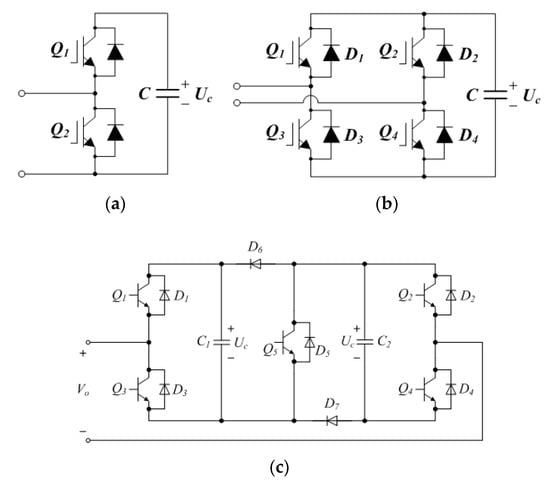
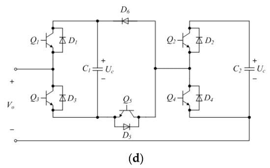
Figure 1.
Circuit configuration of submodules: (a) HBSM, (b) FBSM, (c) CDSM, and (d) IHSM.
The HVDC submodule provides or removes capacitor UC voltage to the converter. The simplest circuit structure is the HBSM in Figure 1a, and the FBSM in Figure 1b allows for a 100% redundancy. The HBSM and FBSM are circuit structures that are faithful to the basic operation of the submodule. However, there is no function to protect submodules from a DC short-circuit current. Figure 1c is a CDSM with one IGBT, two diodes, and one capacitor added to the circuit structure of the FBSM. When a DC short-circuit current occurs, two capacitors absorb the short-circuit current energy and prevent overvoltage by voltage clamping of the added diode [6,11]. The IHSM in Figure 1d has protection against DC short-circuit current and is similar to the CDSM in circuit structure [6,12]. It has five IGBTs, six diodes, and two capacitors. Compared to CDSM, one diode is reduced. However, the circuit operation to absorb the short-circuit current is asymmetric and disadvantageous in terms of short-circuit current energy absorption and overvoltage protection using capacitors rather than CDSM.
2.1. Operational Mode of the IHSM
IHSM is a structure that prevents overvoltage by absorbing short-circuit current energy into capacitors by keeping IGBT Q5 at turn-on in normal mode and turning-off IGBT Q5 when a DC short-circuit current occurs. When a short-circuit current enters the SM (+) terminal, a current path through the two capacitors is formed, but when a short-circuit current is released from the SM (+) terminal, only capacitor C1 absorbs energy.
Figure 2a,b show the current path that charges capacitors C1 and C2 individually in normal mode with which the IHSM is connected to the converter. If the current enters the SM (+) terminal, turning on IGBT Q4 as shown in Figure 2a, capacitor C1 is charged through diode D1 and D5, and turning on IGBT Q3, as shown in Figure 2b, enables the individual charging of capacitor C2 through diodes D2 and D5. The charging of individual capacitors is possible even when IGBT Q5 is in turn-off.
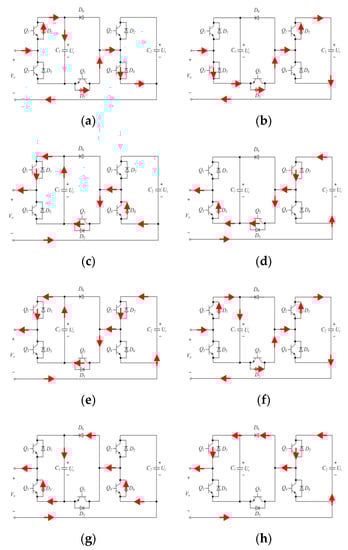
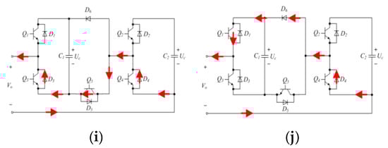
Figure 2.
Operational mode, (a) C1 charging, (b) C2 charging, (c) C1 discharging, (d) C2 discharging, (e) simultaneous discharging, (f) simultaneous charging, (g) C1 charging, (h) C2 discharging, (i) converter disconnected @normal, (j) converter disconnected @abnormal. Note: (a–e) submodule is connected to converter in normal mode, (f–h) submodule is connected to converter in abnormal mode.
Figure 2c,d show the current path when the IHSM individually discharges capacitors C1 and C2 in normal mode connected to the converter. When the current flows from the SM (+) terminal, turning on IGBT Q1 as shown in Figure 2c discharges capacitor C1 through IGBT Q5, diode D4, and turning on IGBT Q2 as shown in Figure 2d enables the individual discharge of capacitor C2 via IGBT Q5 and diode D3. The discharge of individual capacitors is impossible in abnormal mode where IGBT Q5 is turned off.
Figure 2e shows the current path through which the IHSM simultaneously charges capacitors C1 and C2 in normal mode connected to the converter. When the current flows from the SM (+) terminal, turning on IGBT Q1 and Q2, as shown in Figure 2e, capacitors C1 and C2 are simultaneously discharged through IGBT Q5. The simultaneous discharge of capacitors C1 and C2 is impossible in abnormal mode where IGBT Q5 is turned off.
Figure 2f shows the current path through which the IHSM simultaneously charges capacitors C1 and C2 in abnormal mode connected to the converter. This is an operating mode in which DC short-circuit current energy is absorbed into two capacitors and clamped by diode D6 to prevent overvoltage. When current flows into the SM (+) terminal, capacitors C1 and C2 are simultaneously charged through diodes D1, D5, and D2 as shown in Figure 2f. The simultaneous charging of capacitors C1 and C2 is also possible in normal mode with IGBT Q5 on.
Figure 2g,h show the current path when the IHSM charges or discharges capacitors C1 and C2 individually in abnormal mode connected to the converter. When the current flows from the SM (+) terminal, capacitor C1 is charged through diodes D4, D6, and D3, as shown in Figure 2g, and when IGBT Q2 is turned on as shown in Figure 2h, capacitor C2 can be discharged through diodes D6 and D1. The individual charging and discharging of capacitors is only possible when IGBT Q5 is turned off.
Figure 2i,j show the equivalent circuit when the IHSM is disconnected from the converter. When the current flows from the SM (+) terminal, the normal mode in Figure 2i uses the lower current path through diodes D4 and D3 and the abnormal mode has the current path through diodes D4, D6, and D1, as shown in Figure 2j.
2.2. Fault-Tree Design of IHSM
2.2.1. Main Fault Tree
This section describes the design of the fault tree considering the driving characteristics of the IHSM, i.e., the risk of submodule operation including the DC short-circuit current protection. A fault-tree analysis (FTA) is a method of designing a fault tree that logically analyzes the causal relationship of a system failure and finds the probability of a system failure. A logical and probabilistic quantitative failure rate reflecting the operational characteristics of the submodule can be derived.
Figure 3 shows the fault tree taking into account the operational characteristics of the IHSM. Define each sub-stage failure based on the condition that the capacitor of the submodule is connected to or disconnected from the converter. [Capacitor connecting failure] is divided into capacitor charging and discharging failure. [Capacitor charging fault] is designed as an AND-gate combination of [Simultaneous C1 and C2 charging function failure] that charges two capacitors simultaneously and [Individual C1 or C2 charging function failure] that charges separately. The [Simultaneous C1 and C2 charging function failure], which charges two capacitors simultaneously, suppresses overvoltage generation by absorbing energy by two capacitors and clamped by diode D6 in the event of a DC short-circuit current. The [Individual C1 or C2 charging function failure] event is the OR–gate combination of the individual charging function of C1 and C2 in normal mode and the charging function of C1 in abnormal mode, and individual charging of C2 in abnormal mode is impossible. A [C1 or C2 charging function failure] event is the OR-gate combination of the individual charging function of C1 and C2 in normal mode and the charging function of C1 in abnormal mode, and individual charging of C2 in abnormal mode is impossible. When a DC short-circuit current occurs, overvoltage protection is possible through the current path of both capacitors and the current path through which C1 absorbs energy individually. Therefore, it has the AND-gate characteristic that the failure propagates to the higher level only if both functions fail. [Capacitor discharging fault] is designed as an AND-gate combination of events that discharge two capacitors simultaneously and individually.
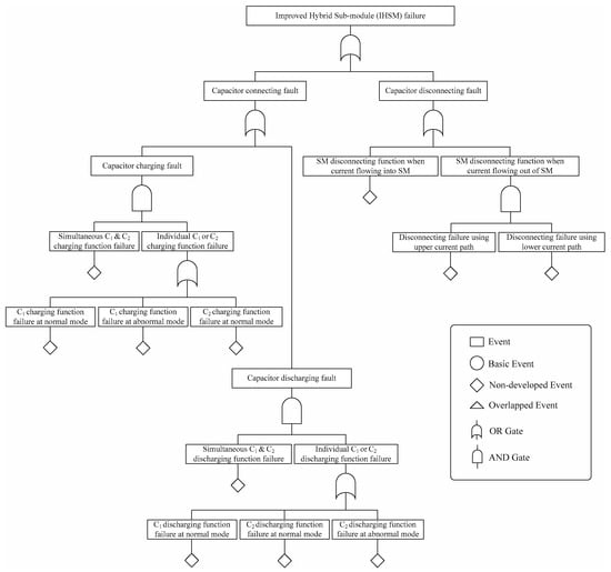
Figure 3.
Main fault tree of improved hybrid submodule (IHSM).
[Individual C1 or C2 discharging function failure] is an OR-gate combination of [C1 discharging function failure at normal mode], [C2 discharging function failure at normal mode], and [C2 discharging function failure at abnormal mode]. The individual discharge of C1 in abnormal mode is impossible. A [Capacitor disconnection failure] event is designed under two conditions: current flowing into or current flowing out from the SM (+) terminal when the submodule capacitor and converter are disconnected. [SM disconnection failure when current flow out of SM] is designed based on the path of current flowing from the SM (+) terminal to the converter when separating the converter from the submodule. It is designed as OR-gate combinations of [Disconnecting failure using upper current path] and [Disconnecting failure using lower current path].
2.2.2. Sub Fault Tree
This section describes the lower level of the fault tree according to the state of the circuit.
Figure 4 is a sub-fault tree for the event of [Simultaneous C1 and C2 charging function failure] that charges two capacitors simultaneously. Five possible events, depending on the operation of the IGBT and diode for generating the current path, consist of an OR-gate combination.
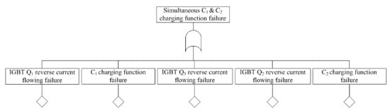
Figure 4.
Sub fault tree for Simultaneous C1 and C2 charging function failure.
Figure 5 shows a sub-fault tree for the event [IGBT Qx reverse current flow failure, x = 1,2]. If it is located at the top of the switch arm, such as IGBT Q1, consider the failure of the switch itself in the lower IGBT Q3, which is joined in series, and the switching signal error.
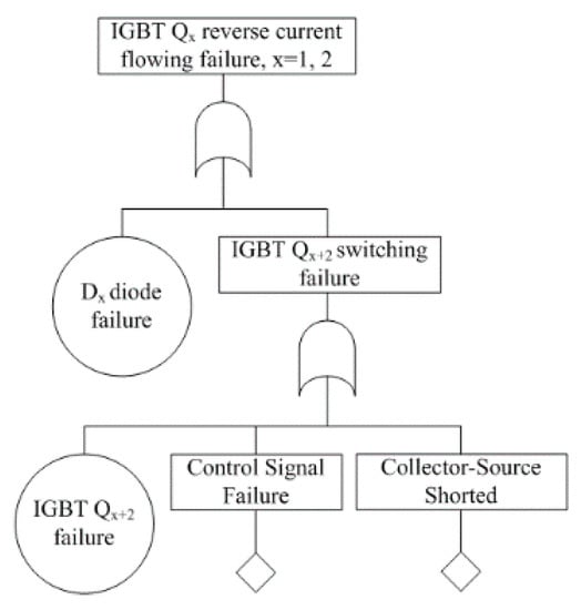
Figure 5.
Sub fault tree for insulated gate bipolar transistor (IGBT) Qx reverse current flowing failure, x = 1,2.
Figure 6 shows the [C1 charging function failure at normal mode] of lower stage failures for the [Individual C1 or C2 charging function failure] event to charge individual capacitors. Four possible failures, depending on the operation of the IGBT and diode for generating the current path, consist of an OR-gate combination.
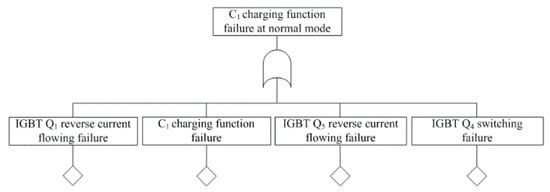
Figure 6.
Sub fault tree for C1 charging function failure at normal mode.
Figure 7 shows the [C2 charging function failure at normal mode] of lower stage failures for the [Individual C1 or C2 charging function failure] event to charge individual capacitors. Four possible failures, depending on the operation of the IGBT and diode for generating the current path, consist of an OR-gate combination.
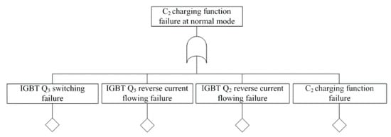
Figure 7.
Sub fault tree for C2 charging function failure at normal mode.
Figure 8 shows the event of charging C1 in abnormal mode during a lower stage failure of [Individual C1 or C2 charging function failure] to charge individual capacitors. It is designed as an OR-gate combination of IGBT-related failures and diode failures that operate to generate current paths.
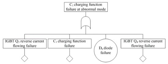
Figure 8.
Sub fault tree for C2 charging function failure at normal mode.
Figure 9 shows the fault tree for the [Simultaneous C1 and C2 discharging function failure] event of discharging two capacitors simultaneously. Five possible failures, depending on the operation of the IGBT and diode for generating the current path, consist of an OR-gate combination.
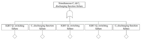
Figure 9.
Sub fault tree for Simultaneous C1 and C2 discharging function failure.
Figure 10 shows the event of [Individual C1 or C2 discarding function failure] among the lower stage failures for the event of discharging individual capacitors. Four possible failures, depending on the operation of the IGBT and diode for generating the current path, consist of an OR-gate combination.
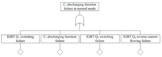
Figure 10.
Sub fault tree for C1 discharging function failure at normal mode.
Figure 11 shows the [C2 discarding function failure at normal mode] of lower stage failure for the [Individual C1 or C2 discarding function failure] event that discharges individual capacitors. Four possible failures, depending on the operation of the IGBT and diode for generating the current path, consist of an OR-gate combination.
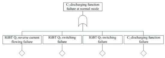
Figure 11.
Sub fault tree for C2 discharging function failure at normal mode.
Figure 12 shows the [C2 discarding function failure at abnormal mode] discharging C2 during sub-stage failures for the [Individual C1 or C2 discarding function failure] event that discharges individual capacitors.
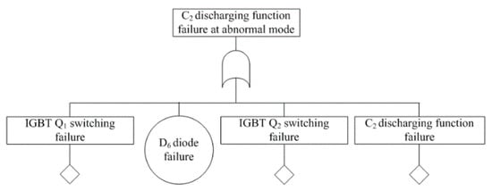
Figure 12.
Sub fault tree for C2 discharging function failure at abnormal mode.
Figure 13 shows a sub-stage failure of the [Capacitor disconnection fault] event in which the capacitor in SM is disconnected from the converter. [SM disconnection function when current flow into SM] is a fault with current flowing into the SM (+) terminal.
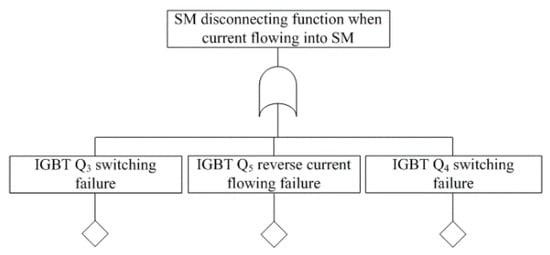
Figure 13.
Sub fault tree for SM disconnecting function when current flowing into SM.
Figure 14 shows a failure in the lower stage of a failure event in which the capacitor in SM is separated from the converter and with current flowing from the SM (+) terminal.
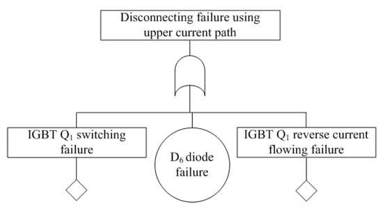
Figure 14.
Sub fault tree for disconnecting failure using upper current path.
Figure 15 shows the failure of the SM capacitor in a lower stage of the failure event of the SM capacitor being separated from the converter and with current flowing from the SM (+) terminal.
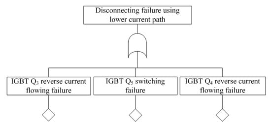
Figure 15.
Sub fault-tree for disconnecting failure using the lower current path.
Figure 16 shows a sub fault tree for the event [IGBT Qx reverse current flow failure, x = 3,4] design with an OR-gate combination of [Dx diode failure] and [IGBT Qx−2 switching failure].
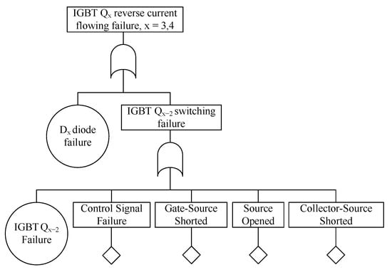
Figure 16.
Sub fault tree for IGBT Qx reverse current flowing failure, x = 3,4.
The [Capacitor Cx charging function failure] and [Capacitor Cx discharging function failure] events in Figure 17 design [Drift] and [Seal failure], which are the major failures of capacitors themselves.
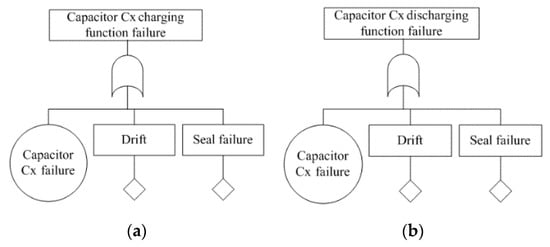
Figure 17.
Sub fault tree for capacitor function failure: (a) charging, (b) discharging.
2.3. Part Failure Rate Based on MIL-HDBK-217F
To calculate the failure rate of the IHSM fault-tree, it is first necessary to calculate the basic component failure rate for the main parts of the submodule, i.e., IGBT, diode, and capacitor. In this paper, the basic failure rate for each part is calculated using the MIL-HDBK-217F failure library [19,20]. The rated power of the IHSM is 2.4 MW, and the rating of the IGBT is 4.5 kV and 1200 A. We add a high-performance diode to parallel the anti-parallel diode inside the IGBT, and the voltage and current ratings are the same as IGBT. The capacitor has an operating voltage of 2750 V at −40 °C to 85 °C. The failure rate is analyzed in an environment where the converter room is controlled at a constant range of 20 °C to 30 °C.
2.3.1. Failure Rate of IGBT
Determine the part failure rate of IGBT from the fact that IGBT consists internally of bipolar junction transistor (BJT) and metal-oxide-semiconductor field-effect transistor (MOSFET) series combinations [8,9,10,21,22,23,24,25]. The failure rate of BJT is as shown in Equation (1).
where λb is the base failure rate (BJT) of 0.00074. πA applies 0.7 as an application factor. πQ is a quality factor, which is 5.5 for commercial use. πE applies 6.0 because the IHSM operates in an environment controlled by the environment factor. πT is a temperature factor. The failure rate of the MOSFET is as shown in Equation (2).
Here, the basic failure rate of MOSFET λb is 0.012, and the rated power is 250 W or higher, so application factor πA applies 10. Quality factor πQ is applied to the commercial product reference value of 5.5 and the environment factor πE is applied to 6.0 because the IHSM operates in a controlled environment. πT is a temperature factor. Since IGBT consists of series combinations of BJT and MOSFET, the failure of either will result in the failure of IGBT. Thus, the failure rate of IGBT can be calculated by Equation (3) through the OR-gate operation of the two elements.
2.3.2. Failure Rate of Diode
For the design of the IHSM, we use fast recovery diode (FRD) to supplement the performance of the internal diode of the IGBT. The failure rate of the diode is as shown in Equation (4).
where the basic failure rate of the diode λb is 0.025, and the contact construction factor πC is 1. Quality factor πQ is applied to the commercial product standard of 5.5, and to the environment factor πE, 6.0 is applied, because the IHSM operates in a controlled environment. πT is a temperature factor.
2.3.3. Failure Rate of Capacitor
Metallized film capacitors that are being utilized in the design of HVDC systems suitable for high power applications are analyzed. The failure rate of capacitors is as shown in Equation (5).
where the basic failure-rate of the Metallized film capacitor (CH) is 0.00037, and the series resistance factor πSR is 1.0. The quality factor πQ is 10, and the environment factor πE is 6.0. πT is a temperature factor.
2.4. Analysis of Failure Rate of IHSM Using Fault-Tree
This section calculates the failure rate of the IHSM by reflecting the part failure rate calculated using MIL-HDBK-217F in the fault tree. Figure 18 shows the failure rate obtained from the fault tree that reflects the operating characteristics of the IHSM, especially the DC short-circuit current protection function. The MTBF (mean time between failures) is expected to be 40,545 h (4.63 years) with 0.247 failures/104 h at 25 °C, and the failure rate of 0.998 failures/104 h at 180 °C shows that the MTBF is reduced to 10,018 h (1.14 years).
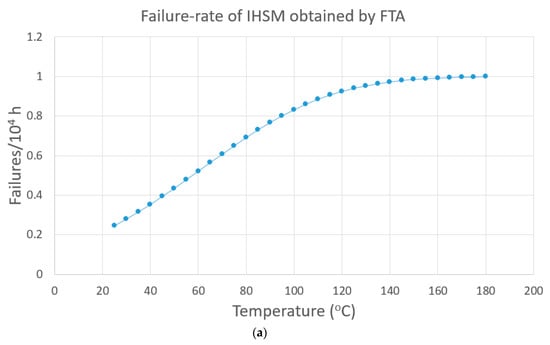
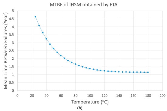
Figure 18.
Failure rate and MTBF (mean time between failures) of IHSM, (a) failure rate, (b) MTBF, year.
2.5. Comparison of HBSM, FBSM, CDSM, and IHSM
2.5.1. Comparison of Failure Rate
This chapter compares the failure rate of the FTA, which reflects the operational characteristics and risks of the submodule, with the failure rate calculated by the part count failure analysis (PCA). A comparative analysis of submodules is made when the same design conditions are applied [8,9,10]. The IHSM has a DC short-circuit current protection function and is a circuit structure with one diode reduced in the structure of the CDSM, and one IGBT, two diodes, and one capacitor increased compared to the FBSM.
For PCA, even one component of a submodule can be seen as a failure of a submodule if it fails, so each component has the characteristics of a parallel relationship failure as given in Figure 19. In other words, the PCA obtained the failure rate of the submodule by considering only the type, number, and coupling of IGBT, diode, and capacitor parts.
Figure 19.
Reliability dependance of IHSM for part count failure analysis (PCA).
Figure 20a shows the results of PCA-based failure rate comparison. Since the PCA method is a reliability evaluation that only considers the type, number, and connection status of parts, the failure rate usually increases as the number of parts increases. Since only the number of parts differs under the same conditions, the failure rate is high in the order of CDSM > IHSM > FBSM > HBSM with the most parts. CDSM and IHSM represent a difference in the number of parts per diode, with a near similar failure rate, but CDSM has a slightly higher failure rate than IHSM.
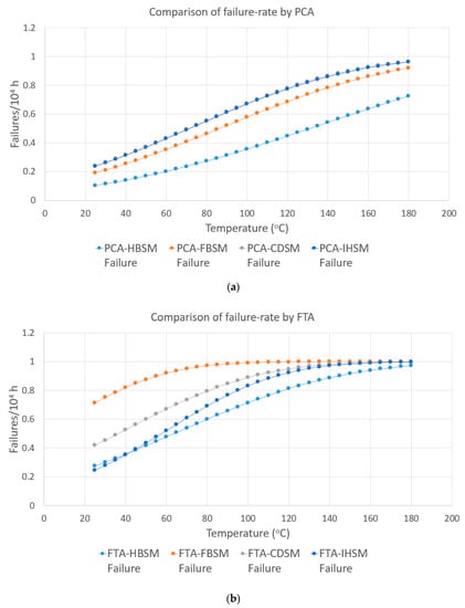
Figure 20.
Comparison of failure rate and MTBF, (a) PCA-based, (b) fault-tree analysis (FTA)-based.
The FTA-based analysis, which takes into account the operational characteristics of the submodules in Figure 20b, indicates that the failure rate is high in the order of FBSM > CDSM > IHSM > HBSM. The addition of DC short-circuit current protection has the effect of improving reliability, but the reliability of CDSM is generally lower than that of HBSM due to the increase in the number of parts. It is noteworthy that the IHSM has a lower failure rate than the HBSM at 40 °C or below, confirming that the DC short-circuit current protection function is sufficient to improve reliability. This means that in the converter room, which is controlled by an average of 25 °C, the number of parts with the DC short-circuit current protection function increases significantly compared to the HBSM, so the failure rate should generally be increased, but the DC short-circuit current protection function has the effect of improving reliability by lowering the failure rate.
2.5.2. Comparison of the Number of Parts
Figure 21 shows a comparison of the number of parts in the HBSM, FBSM, CDSM, and IHSM. In the IGBT and diode comparison in Figure 21a, the HBSM has the smallest number of parts. The number of parts of the submodule with DC short-circuit current protection generally has the largest number of parts, and the CDSM has the largest number of semiconductor devices. Figure 21b shows that the CDSM and IHSM have two capacitors, and the remaining submodules require one capacitor. CDSM and IHSM use two capacitors to effectively inhibit overvoltage generation and to absorb short-circuit current energy, so it cannot be simply assumed that an increase in the number of capacitor parts is uneconomical.
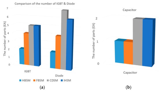
Figure 21.
Comparison of the number of components, (a) IGBT, diode, (b) capacitor.
2.5.3. Comparison of Voltage and Current Stress for Switching Devices
Figure 22 compares the voltage and current stresses applied to switching devices according to the structure of the submodule. Temporary surge voltage by switching and over-current by DC short circuit are excluded from analysis and compared based on the average voltage and average current. At 2.4 MW, the voltage stress of IGBT and diodes in HBSM, FBSM, CDSM, and IHSM is the same at 2400 V, and the current stress is 1000 A, requiring the same current rating.
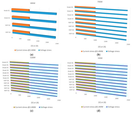
Figure 22.
Comparison of voltage and current stress on the switching devices, (a) half-bridge submodule (HBSM), (b) full-bridge submodule (FBSM), (c) clamped-double submodule (CDSM), (d) improved hybrid submodule (IHSM).
Figure 23a shows the analysis of the failure rate of the IHSM according to the PCA method. A smaller voltage margin indicates a proportional increase in the failure rate. However, PCA results alone make it difficult to determine the appropriate voltage margin of the switching device. Figure 23b shows the results of the failure rate analysis of the FTA method for the IHSM when changing the voltage margin of the switching device. The smaller the voltage margin, the more proportionally increasing the failure rate, and the relatively significant reduction in the failure rate when the voltage margin is set at 2.5 times. However, when applying IGBT and diodes with a 2.5× voltage margin, the problem of the component price increases, and efficiency degradation relative to reduced failure rates should be considered.
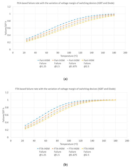
Figure 23.
Failure rate according to the voltage margin of circuit components, (a) PCA-based, (b) FTA-based.
Figure 24 analyzes the failure rate according to the working voltage margin of the capacitor of the IHSM. The switching device (IGBT and diode) is fixed at 1.875 times the voltage rating, and the failure rate is analyzed when the capacitor working voltage margin is changed to 1.04, 1.08, 1.15, 1.25, and 2.5 times. Changing the capacitor working voltage margin with the voltage margin of 1.875 times for the IGBT and diode has little effect on the overall failure rate of the IHSM. Therefore, if capacitors are designed to have a 1.15× working voltage margin, they are not significantly affected in terms of failure rates and can change the working voltage margin of capacitors considering the average applied voltage, cost, size, and volume.
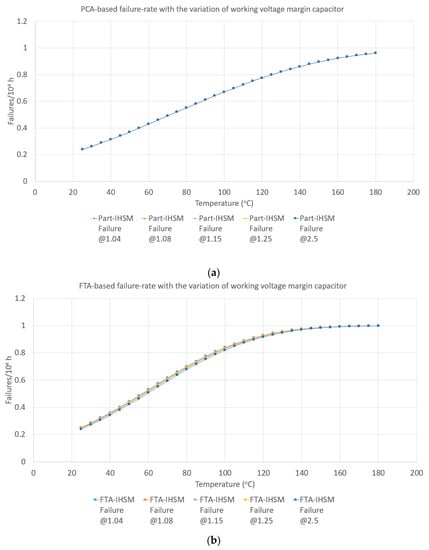
Figure 24.
Failure rate with the variation of working voltage margin of capacitor, (a) PCA-based, (b) FTA-based.
3. Conclusions
In this paper, we analyze the failure rate of IHSM with DC short-circuit current protection using fault tree and how increasing the number of parts and protection functions affect the failure rate. PCA shows high failure rates in the order of CDSM > IHSM > FBSM > HBSM. However, the results of the FTA show high failure rates in the order of FBSM > CDSM > IHSM > HBSM.
In particular, when the submodule operates in a converter room controlled at an average temperature of 25 °C, it can be seen that the number of parts in the IHSM increases significantly compared to that of the HBSM but has a lower failure rate. This is a result of IHSM’s DC short-circuit protection that can inhibit the increase in failure rates as the number of parts increases. This also shows that FTA, which can reflect the operational characteristics of submodules, are a more advanced analysis method than PCA that simply considers the number of parts, types, and connecting status.
In addition, the failure-rate comparison results, considering the number of parts in the submodule, the voltage, and current stress applied to the switching devices, and the voltage margin, provide guidance from various perspectives for submodule selection.
Author Contributions
Conceptualization, F.-S.K. and S.-G.S.; methodology, F.-S.K.; software, F.-S.K.; validation, S.-G.S.; formal analysis, F.-S.K.; investigation, F.-S.K.; data curation, S.-G.S.; writing—original draft preparation, F.-S.K. and S.-G.S.; writing—review and editing, F.-S.K. and S.-G.S. All authors have read and agreed to the published version of the manuscript.
Funding
This research received no external funding.
Conflicts of Interest
The authors declare no conflict of interest.
Abbreviations and Acronyms
| BJT | Bipolar Junction Transistor |
| CDSM | Clamped-Double Submodule |
| FBSM | Full-Bridge Submodule |
| FTA | Fault-Tree Analysis |
| FRD | Fast Recovery Diode |
| HBSM | Half-Bridge Submodule |
| HVDC | High Voltage Direct Current |
| IGBT | Insulated Gate Bipolar Transistor |
| IHSM | Improved Hybrid Submodule |
| MOSFET | Metal-Oxide-Semiconductor Field-Effect Transistor |
| MTBF | Mean Time between Failures |
| PCA | Part Count Failure Analysis |
| SM | Submodule |
| UC | Voltage Across the Capacitor of Submodule |
| λb | The Base Failure Rate of Part |
| πA | Application Factor of BJT |
| πC | The Contact Construction Factor of Diode |
| πE | Environment Factor |
| πQ | Quality Factor |
| πSR | The Series Resistance Factor of Capacitor |
| πT | Temperature Factor |
References
- Billinton, R.; Khan, E. A Security Based Approach to Composite Power System Reliability Evaluation. IEEE Trans. Power Syst. 1992, 7, 65–72. [Google Scholar] [CrossRef]
- Choi, J.; Kim, H.; Cha, J.; Billinton, R. Nodal Probabilistic Congestion and Reliability Evaluation of a Transmission System under the Deregulated Electricity Market. In Proceedings of the IEEE PES SM2001 Conference, Vancouver, BC, Canada, 15–19 July 2001. [Google Scholar]
- Xu, J.; Jing, H.; Zhao, C. Reliability Modeling of MMCs Considering Correlations of the Requisite and Redundant submodules. IEEE Trans. Power Deliv. 2018, 33, 1213–1222. [Google Scholar] [CrossRef]
- Alharbi, M.; Isik, S.; Bhattacharya, S. Reliability Comparison and Evaluation of MMC Based HVDC Systems. In Proceedings of the 2018 IEEE Electronic Power Grid (eGrid), Charleston, SC, USA, 12–14 November 2018. [Google Scholar]
- Guo, J.; Liang, J.; Zhang, X.; Judge, P.D.; Wang, X.; Green, T.C. Reliability Analysis of MMCs Considering Submodule Designs with Individual or Series-Operated IGBTs. IEEE Trans. Power Deliv. 2017, 32, 666–677. [Google Scholar] [CrossRef]
- Xu, J.; Zhao, P.; Zhao, C. Reliability Analysis and Redundancy Configuration of MMC with Hybrid Submodule Topologies. IEEE Trans. Power Elect. 2016, 31, 2720–2729. [Google Scholar] [CrossRef]
- Dong, Y.; Yang, H.; Li, W.; He, X. Neutral-Point-Shift-Based Active Thermal Control for a Modular Multilevel Converter Under a Single-Phase-to-Ground Fault. IEEE Trans. Ind. Electron. 2019, 66, 2474–2484. [Google Scholar] [CrossRef]
- Kang, F.S.; Song, S.G. Fault-tree Analysis Based Life-cycle Expectation for Half-bridge Submodule in HVDC. Trans. Korean Inst. Elect. Eng. 2020, 69, 42–49. [Google Scholar] [CrossRef]
- Kang, F.S.; Song, S.G. Life-cycle estimation of HVDC full-bridge sub-module considering operational condition and redundancy. Trans. Inst. Korean Elect. Electron. Eng. 2019, 23, 1208–1217. [Google Scholar]
- Kang, F.S.; Song, S.G. Fault-tree based reliability analysis for paralleled half-bridge sub-module of HVDC. Trans. Inst. Korean Elect. Electron. Eng. 2019, 23, 1218–1223. [Google Scholar]
- Marquardt, R. Modular Multilevel Converter: A Universal Concept for HVDC-Networks and extended DC-Bus-applications. In Proceedings of the International Power Engineering Conference (IPEC), Sapporo, Japan, 21–24 June 2010. [Google Scholar]
- Zhang, J.; Zhao, C.; Guo, L. Simulation analysis on submodule topology of modular multilevel converter. Autom. Electr. Power Syst. 2015, 39, 106–111. [Google Scholar]
- Zhao, P.; Wang, C.; Xu, J.; Zong, B.; Zhao, C. A sub-module technology of MMC with DC fault ride-through capability. Power Syst. Technol. 2015, 38, 106–111. [Google Scholar]
- Yang, S.; Bryant, A.; Mawby, P.; Xiang, D.; Ran, L.; Tavner, P. An Industry-Based Survey of Reliability in Power Electronic Converters. IEEE Trans. Ind. Appl. 2011, 47, 1441–1451. [Google Scholar] [CrossRef]
- Song, Y.; Wang, B. Survey on Reliability of Power Electronics Systems. IEEE Trans. Power Electron. 2013, 28, 591–604. [Google Scholar] [CrossRef]
- Denson, W. The history of reliability prediction. IEEE Trans. Reliab. 1998, 47, 321–328. [Google Scholar] [CrossRef]
- Wang, Y.D.; Song, B.F. Overview of system reliability prediction method. Aircr. Des. 2008, 28, 37–42. [Google Scholar]
- Li, Y.H. A brief analysis about the guide and standard of reliability prediction and estimation for electronic system and equipment. Aeronaut. Stand. Qual. 2006, 1, 50–54. [Google Scholar]
- Mou, H.; Hu, W.; Sun, Y.; Zhao, G. A Comparison and Case Studies of Electronic Product Reliability Prediction Methods Based on Handbooks. In Proceedings of the International Conference on Quality, Reliability, Risk, Maintenance, and Safety Engineering (QR2MSE), Chengdu, China, 15–18 July 2013; pp. 112–115. [Google Scholar]
- Jones, J.; Hayes, J. A comparison of electronic-reliability prediction models. IEEE Trans. Reliab. 1999, 48, 127–134. [Google Scholar] [CrossRef]
- Cushin, M.J.; Mortin, D.E.; Stadterman, T.J.; Malhotra, A. Comparison of Electronics-Reliability Assessment Approaches. IEEE Trans. Reliab. 1993, 42, 542–546. [Google Scholar] [CrossRef]
- Reliability Prediction of Electric Equipment. Department of Defense, Washington DC, Tech. Rep. MIL-HDBK-217F, Dec. 1991. Available online: http://everyspec.com/MIL-HDBK/MIL-HDBK-0200-0299/MIL-HDBK-217F_14591 (accessed on 8 January 2021).
- Choudhary, K.; Sidharthan, P. Reliability Prediction of Electronic Power Conditioner (EPC) using MIL-HDBK-217 based Parts Count Method. In Proceedings of the 2015 International Conference on Computer, Communication and Control (IC4), Indore, India, 10–12 September 2015. [Google Scholar]
- Lambilly, H.; Keser, H.O. Failure Analysis of Power Modules: A Look at the Packaging and Reliability of Large IGBT’s. IEEE Trans. Compon. Hybrids Manuf. Tech. 1993, 16, 412–417. [Google Scholar] [CrossRef]
- Valentine, N.; Das, D.; Pecht, M. Failure Mechanisms of Insulated Gate Bipolar Transistors (IGBTs). In NREL Photovoltaic Reliability Workshop; 2015. Available online: https://www.nrel.gov/pv/assets/pdfs/2015_pvmrw_131_das.pdf (accessed on 8 January 2021).


Publisher’s Note: MDPI stays neutral with regard to jurisdictional claims in published maps and institutional affiliations. |
© 2021 by the authors. Licensee MDPI, Basel, Switzerland. This article is an open access article distributed under the terms and conditions of the Creative Commons Attribution (CC BY) license (http://creativecommons.org/licenses/by/4.0/).