Article

Systematical Study of the Basic Properties of Surface Acoustic Wave Devices Based on ZnO and GaN Multilayers

Key Laboratory of Advanced Materials (MOE), School of Materials Science and Engineering, Tsinghua University, Beijing 100084, China
*
Authors to whom correspondence should be addressed.
Electronics 2021, 10(1), 23; https://doi.org/10.3390/electronics10010023
Submission received: 28 November 2020 / Revised: 21 December 2020 / Accepted: 23 December 2020 / Published: 25 December 2020

Abstract

:
Recently, surface acoustic wave (SAW) devices based on layered structures are a popular area of research. Multilayered structures, including ZnO and GaN, have shown great performance and can be applied in diverse fields. Meanwhile, thin films, such as AlGaN and n-ZnO, can be added to these structures to form a 2-D electron gas (2DEG) which makes the devices tunable. This work systematically studies the basic properties of SAW devices based on ZnO and GaN multilayers via COMSOL Multiphysics. The sorts of structures with different crystal orientations are simulated, and various acoustic modes are considered. Results show that a range of phase velocity from about 2700 m/s to 6500 m/s can be achieved, and devices based on ZnO and GaN multilayers can meet the requirements of the electromechanical coupling coefficient from about 0 to 7%. Every structure’s unique properties are valuable for diverse applications. For example, c-ZnO/c-GaN/c-sapphire structure can be used for high-frequency and large-bandwidth SAW devices, while SAW devices based on a-ZnO/a-GaN/r-sapphire and 2DEG are suitable for programmable SAW sensors. This work has great reference value for future research into SAW devices.

1. Introduction

Surface acoustic wave (SAW) devices have received great attention in the field of wireless communication and sensing applications for decades, because of their small size and reliable performance [1,2,3,4,5]. Conventional SAW devices are fabricated on piezoelectric substrates, such as LiNbO3, LiTaO3, and quartz. Unfortunately, the acoustic velocities of these piezoelectric substrates are relatively low [6] for high-frequency SAW devices, which is imperative in the 5G era, and performances of SAW devices based on these substrates are hard to optimize because their structures are single. Using layered structures with piezoelectric thin film and substrate with high acoustic velocity is a possible solution.
ZnO, a multi-functional material [7,8,9], has considerable piezoelectricity, which is suitable for piezoelectric thin film in SAW devices. Plenty of research about SAW devices based on ZnO thin film and substrates with high acoustic velocities has been published. High frequency can be obtained in ZnO/diamond or the ZnO/SiC structure as the acoustic velocities of diamond and SiC are extremely high [10,11,12]. However, diamond and SiC substrates are expensive, which limits the applications. Compared to diamond and SiC, sapphire wafer is much cheaper, and the acoustic velocity is also very high. Furthermore, the acoustic attenuation loss is low, and the orientation of sapphire substrate is abundant, so ZnO thin films with different orientations can be grown on various sapphire substrates. These thin films with various SAW properties are appropriate for diverse applications. For example, shear-horizontal (SH) SAW, which can be converted to Love-mode wave [13,14], is suitable for sensing in liquid environments [15,16]. A-plane ZnO (a-ZnO) can be deposited on r-plane sapphire (r-sapphire) substrate, in which Love-mode SAW can be excited [17]. Different types of SAW devices based on c-ZnO/c-sapphire or a-ZnO/r-sapphire have been theoretically or experimentally studied [18,19,20,21], verifying the huge value of the ZnO/sapphire structure.
Nevertheless, there exists a relatively large mismatch of lattice constants between ZnO thin film and sapphire substrate, limiting the crystal quality of ZnO thin film and leading to the propensity of ZnO to crack [22,23,24]. A promising solution is using GaN as a buffer layer because the crystal structure types of ZnO and GaN are both hexagonal and their lattice constants are very close [22,23,24]. By adopting a-GaN buffer layer, many researchers have successfully deposited high-quality and strongly oriented ZnO thin film [22,23,24]. Therefore, ZnO/GaN/sapphire multilayered structure is appropriate for SAW devices.
Meanwhile, researchers are pursuing programmable and adaptive applications in wireless communication and sensing systems, so developing tunable SAW devices is necessary. One way to realize tunable SAW devices refers to high electron-mobility transistors (HEMT). The acoustoelectric effect, which is where free carriers in a nearby semiconductor affect the amplitude and phase velocity of SAW [25,26,27], is used. AlGaAs/GaAs, AlGaN/GaN and n-ZnO/GaN heterostructures were introduced into SAW devices and considerable tunabilities were achieved [28,29,30,31]. This kind of tunable device can be treated as adding one thin layer of AlGaN or n-ZnO into the normal ZnO/GaN structure, which is a basic structure of tunable SAW devices. Compared with the films in normal SAW devices, the layer of AlGaN or n-ZnO in the heterostructure is usually very thin, so that the layer does not highly influence the basic SAW performance. Therefore, the basic SAW properties are still decided by the ZnO/GaN structure, and the 2-D electron gas (2DEG) makes SAW devices tunable. Analyzing the basic ZnO/GaN structure is the foundation.
Former analysis shows that structures with ZnO and GaN multilayers are of great value in high-frequency SAW devices, SAW sensors, tunable SAW devices, and so on. However, there are still some valuable structures with ZnO and GaN multilayers which have not been proposed and studied. Meanwhile, a study of basic SAW properties, which covers as many structures and wave modes as possible, is helpful for future research. In this work, we systematically research the basic properties of SAW devices based on ZnO and GaN multilayers including a-ZnO/a-GaN, a-ZnO/a-GaN/r-sapphire, c-ZnO/c-GaN, c-ZnO/c-GaN/c-sapphire, and c-ZnO/SiNx/GaN, etc. These structures are all feasible to be fabricated in reality according to the former research [17,18,19,20,21,22,23,24,32]. Basic characteristics of Rayleigh-mode waves, Sezawa-mode waves, and Love-mode waves, which are appropriate for various applications, have been studied. This work is a reference for research about diverse SAW devices based on ZnO and GaN multilayers in the future.

2. Methods

All the structures are theoretically studied by the finite element method (FEM) via COMSOL Multiphysics software. Models with only one period and side face, where periodic boundary condition is set, are simulated. One of the electrodes is electrically grounded and the other one is terminal. The Euler angle (α, β, γ) which describes three successive rotations can achieve any spatial orientations. C-plane orientation, also known as (0001) plane orientation, is the normal one, so the corresponding Euler angle is (0, 0, 0), which means that the local coordinate systems do not need to be rotated. A-plane is (11 2 ¯ 0) plane. To obtain a-plane, the Euler angle of (α, 90°, 0°) should be set. Two-dimensional (2D) models are used in the simulation of devices based on c-ZnO or c-GaN because the rotation is unnecessary and the displacement in the transverse direction is negligible. We use three-dimensional (3D) model to simulate devices based on a-ZnO, and the Euler angle of (90°, 57.6°, 150°) is defined to achieve sapphire substrate with r-plane [17]. The Euler angles of (0°, 90°, 0°) and (90°, 90°, 0°) corresponds to the a-ZnO or a-GaN with propagation directions of [1 1 ¯ 00] and [0001], respectively [17]. The material constants are cited from references [33,34] and the material library in COMSOL.
In this work, h and λ stand for the thickness and the wavelength, respectively. The phase velocity (vp) and the electromechanical coupling coefficient (K2) are calculated from:
v p = ( f r + f a ) × λ 2
K 2 = π f r / ( 2 f a ) tan [ π f r / ( 2 f a ) ]
where fr is the resonance frequency and fa is the anti-resonance frequency [35,36]. Al is chosen as the material of electrodes in this work and the thicknesses of the electrodes are all 0.08λ. All the parameters adopted in the FEM studies are shown in Table 1.
To accurately study the propagation properties, we show displacement curves and deformation shapes of the excited SAW. Deformation shapes intuitively describe vibration states. Displacement (u) has three components, including ux, uy, and uz. The displacement curve shows the normalized displacement at every point on an imaginary perpendicular line passing straight through the whole model from the middle of one electrode in the anti-symmetric state. For three-dimensional models, ux, uy, and uz are all shown in the displacement curves, while only ux and uz are depicted for two-dimensional ones.

3. Results

At first, SAW devices based on a-ZnO are studied because different modes of SAW can be used in various propagation directions [17]. When a-GaN substrate is directly adopted or a-GaN thin film is much thicker than the propagation area of SAW, the SAW devices have a-ZnO/a-GaN bilayer structure.

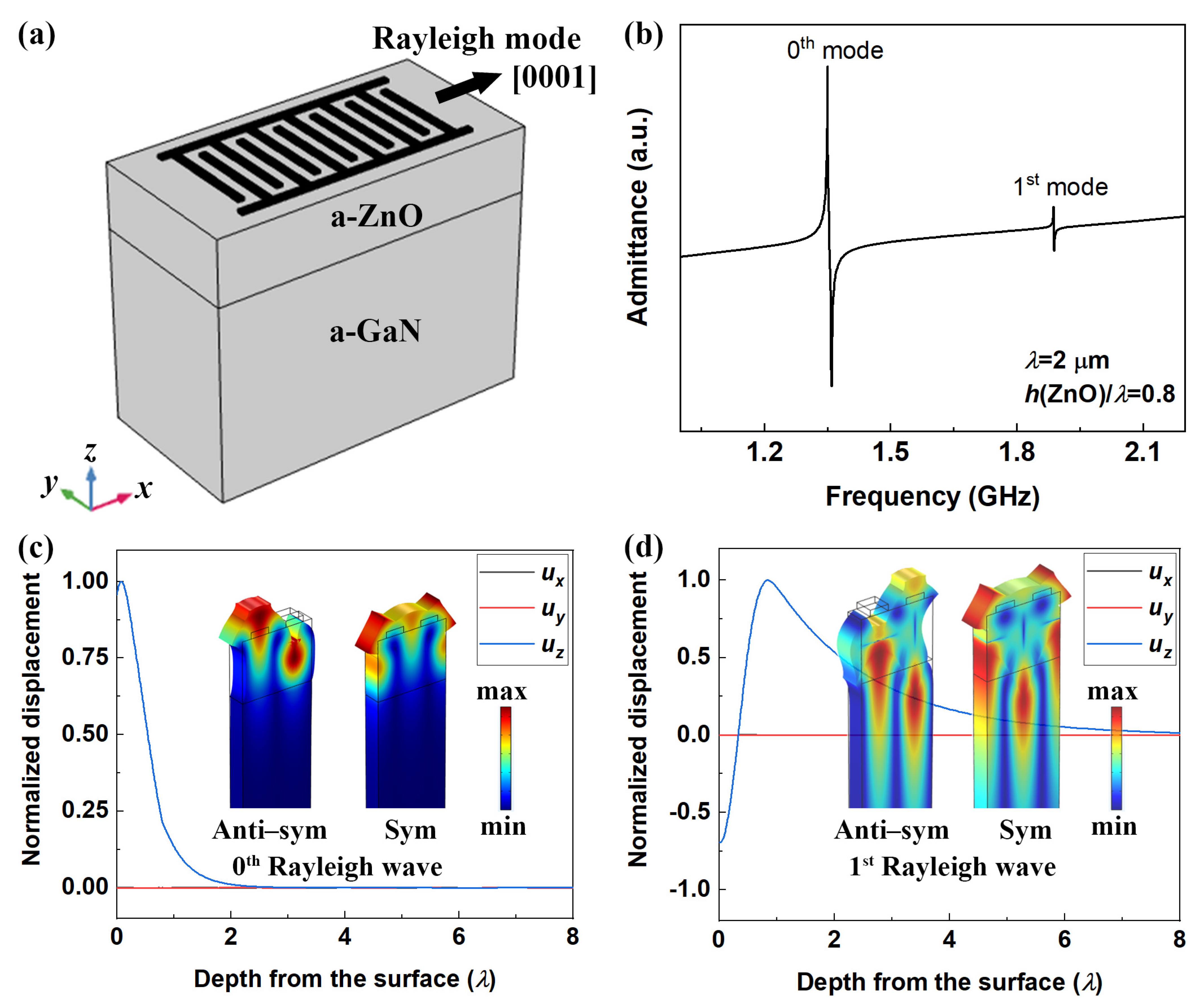
3.1. Devices Based on a-ZnO/a-GaN

A typical admittance response in the structure shown in Figure 1a is depicted in Figure 1b, in which λ is 2 μm and the ZnO thickness is 0.8λ. The frequency of the 0th mode wave is about 1.3 GHz and that of the 1st mode wave is about 1.7 GHz. To ensure the modes of excited SAW and determine the propagation characteristics, we show the displacement curves and the corresponding deformation shapes in Figure 1c,d. It can be clearly seen that the displacements only focus on the y direction. Considering the x propagation direction, we can identify that the SAW is SH wave. As the phase velocity of GaN is higher than that of ZnO [37], ZnO can be regarded as the waveguiding layer of the SH-SAW. We can more precisely call it Love-mode wave. Figure 1c shows the displacement curves, the deformation shapes in anti-symmetric (anti-sym) and symmetric (sym) states of the SAW corresponding to the 0th mode in Figure 1b. The displacement reaches its maximum at the surface and reduces dramatically beneath the surface. The wave only penetrates about 2λ below the surface. For higher order modes, deformation shapes are more complicated. Figure 1d, corresponding to the 1st mode in Figure 1b, shows that the penetration is deeper, but the wave still focuses on the surface.
When the propagation direction rotates 90°, the responses change totally, as shown in Figure 2. Figure 2b depicts a typical admittance curve, in which the 1st mode response becomes weak. Figure 2c,d show that the wave only vibrates in the XZ plane and in a shape of ellipse, so Rayleigh-mode wave is excited. 0th mode wave only propagates in the surface region with the depth about 2λ, as in Figure 2c, but the 1st mode wave penetrates deeply. A large amount of energy loses when the 1st mode Rayleigh wave is excited, leading to a weak response.
The vp and K2 dispersion patterns of the Love-mode waves in Figure 1 are shown in Figure 3a. The values of vp of the first two orders both decrease monotonically with the increase of the ZnO thickness because the smaller phase velocity of a-ZnO. The values of K2 of 0th mode Love wave are quite large, and a maximum value which is larger than 5% appears at h(ZnO)/λ = 0.3 when the vp is about 3000 m/s. The cutoff point of the 1st mode Love wave is at about h(ZnO)/λ = 0.5. The values of vp of the 1st mode wave are relatively large, but the values of K2 are smaller compared with those of the 0th mode. The maximum value of K2 is still smaller than 2%. Figure 3b shows the properties of the Rayleigh-mode waves in Figure 2 as functions of the ZnO thickness. The vp of each mode also decreases when the ZnO thickness is larger. In the meantime, the values of K2 of the Rayleigh-mode waves are smaller than those of the Love-mode waves in Figure 3a. When the ZnO thickness is larger than 1λ, the values of K2 of the 0th mode Rayleigh wave stabilize at the value about 1.9% and the values of vp stabilize around 2700 m/s. The K2 of the 1st mode wave is quite small, just as expected, and the cutoff point is at about h(ZnO)/λ = 0.7.

3.2. Devices Based on a-ZnO/a-GaN/r-Sapphire

When the thickness of GaN thin film is comparable to the wavelength or even thinner, the influence from the sapphire substrate must be considered, so the structure shown in Figure 4a is studied. A typical admittance curve, in which λ, h(ZnO) and h(GaN) are 2 μm, 0.5λ and 0.5λ, respectively, is shown in Figure 4b. The frequency of the 0th mode wave reaches about 1.4 GHz and the 1st mode wave with the frequency of around 2 GHz is excited. The corresponding displacement curves and deformation shapes are shown in Figure 4c,d where the vibration states are similar to those in Figure 1c,d, so the SAW can be identified as the Love-mode wave. As the sapphire substrate with higher acoustic velocity has stronger effect of wave confinement than GaN, the propagation region in the a-ZnO/a-GaN/r-sapphire structure is shallower than that in the a-ZnO/a-GaN structure, which can be seen in Figure 1 and Figure 4.
The values of vp and K2 of the Love-mode waves in Figure 4 are calculated as functions of h(ZnO) and h(GaN), and the results are shown in Figure 5. The values of vp of both modes decrease clearly with the increasing h(GaN), because the acoustic velocity of GaN is smaller than that of sapphire. The values of K2 of 0th mode are not highly influenced by the GaN thickness, which can be seen in Figure 3a and Figure 5. It proves that the ZnO layer mainly converts the energy during Love wave excitation, and the GaN layer and the sapphire layer both only propagate the wave. Nevertheless, the response of 1st mode wave is a little different from that in the a-ZnO/a-GaN structure which has a cutoff point. Even when the ZnO thickness equals 0.1λ, 1st mode Love SAW is still excited, owing to the strong effect of wave confinement from the sapphire substrate. The values of K2 of the 1st mode are still smaller than 2%, which is same as the a-ZnO/a-GaN structure. On the other hand, the values of vp of both modes decrease and approach to the acoustic velocity of ZnO with the thickness increase of ZnO thin film. The K2 of the 0th mode increases at first and then decreases when the ZnO film is thickened, causing a maximum value close to 6% at h(ZnO)/λ = 0.3.
SAW devices based on the a-ZnO/a-GaN/r-sapphire structure with the propagation direction of [0001] have not been studied, because we believe that they are not actually valuable. There are too many SAW responses in these devices and these responses are influenced with each other. Moreover, if we want to obtain Rayleigh wave response, fabricating SAW devices based on c-ZnO is a great choice.

3.3. Devices Based on c-ZnO/c-GaN

The propagation direction of devices based on c-ZnO does not highly influence the properties of SAW, so we only study the devices based on c-ZnO with one normal propagation direction. Figure 6a shows the basic c-ZnO/c-GaN structure and Figure 6b depicts a typical admittance response when the λ is 2 μm and the ZnO thickness is 0.8λ. The frequencies of the 0th mode and 1st mode are about 1.35 GHz and 1.85 GHz, respectively, close to those of Love-mode waves in devices based on the a-ZnO/a-GaN structure. Figure 6c shows the displacement curves and the deformation shapes of the 0th mode wave and Figure 6d shows the ones of the 1st mode. Two-dimensional models are simulated for devices based on c-ZnO, as we discussed before, so only the curves of ux and uz are drawn in Figure 6c,d. The deformation shapes and displacement curves indicate that the responses come from the 0th mode Rayleigh wave and the 1st mode Rayleigh wave. The 0th mode penetrates about 2λ deep, but 1st mode deeper than 4λ. The 1st mode Rayleigh wave is still a stable SAW because it is non-leaky, even though it penetrates a lot.
To systematically study the structure in Figure 6a, we calculate the vp and K2 of the Rayleigh-mode waves in devices with the variation of h(ZnO) and depict the results in Figure 7. With the increase of the ZnO thickness, the values of vp of two modes decrease, same as the tendencies in Figure 3 and Figure 5 for the same reason. When h(ZnO) rises, the K2 of the 0th mode decreases at first and then increases until reaching the maximum value of about 1.05%. For the 0th mode waves in the devices with h(ZnO) larger than 1.5λ, the values of vp and K2 stabilize at about 2700 m/s and 1.05%, respectively. For the 1st mode wave, there exists a cutoff point at about h(ZnO)/λ = 0.5 and exists a maximum value of about 0.8% at about h(ZnO)/λ = 0.9. The values of K2 are relatively small in the devices based on the structure in Figure 6a, which can be clearly seen in Figure 7.

3.4. Devices Based on c-ZnO/c-GaN/c-Sapphire

Now we consider the situation in which GaN is a thin film. The c-ZnO/c-GaN/c-sapphire structure is depicted in Figure 8a and a typical admittance curve is shown in Figure 8b. When the λ, h(ZnO) and h(GaN) equal 2 μm, 0.5λ, 0.5λ, respectively, the 0th mode response is excited at the frequency of about 1.5 GHz and the 1st mode at about 2.2 GHz. The corresponding deformation shapes and normalized displacement curves are shown in Figure 8c,d. According to the previous analysis, Rayleigh-mode waves are excited in this structure. Same as the wave in Figure 6c, the 0th mode wave in Figure 8c also propagates in the region near the surface. However, if we compare Figure 6d with Figure 8d, differences appear. GaN layer cannot highly confine the wave because the acoustic velocities of GaN and ZnO are close, resulting in obvious displacements even at 4λ beneath the surface. The acoustic velocity of sapphire is much larger, so it dramatically confines the 1st mode wave. The so-called “slow-on-fast” structure makes the 1st mode Rayleigh wave become a confined mode which is specifically called Sezawa-mode [38,39,40].
The vp and K2 dispersion patterns of the 0th mode Rayleigh wave in Figure 8 are shown in Figure 9a,b. The values of vp decrease monotonically with the increase of h(ZnO), while those of K2 decrease at first and then increase. These tendencies are similar to those of the same mode in Figure 7. In the devices with the ZnO film thinner than about 0.8λ, the values of vp decrease and approach to the values of the same mode in Figure 7 with the increasing thickness of GaN. It verifies that the sapphire substrate has the function of frequency improvement. Still in these devices, the values of K2 increase and get close to those in Figure 7 when the GaN thickness is thickened from 0.25λ to 1.0λ. We believe that the GaN which is also a piezoelectric material can convert energy to some extent during the Rayleigh-mode excitation, so thickening GaN helps increase the K2 when the ZnO layer is thin. The ZnO layer mainly excites and propagates the wave if it is thick, then the values of vp and K2 do not change much with the variation of h(GaN).
The vp and K2 of the 1st mode Rayleigh wave (Sezawa-mode wave) as functions of the thicknesses of ZnO and GaN are shown in Figure 9c,d. There is no cutoff point in this structure. The values of vp and K2 both decrease and approach to the values in Figure 7 with the increase of h(GaN), because the GaN layer hampers the sapphire’s abilities to improve the vp and confine the wave. When the ZnO thickness is thickened, the values of vp decrease monotonically, and those of K2 increase at first and then decrease. At h(ZnO)/λ = 0.3 and h(GaN)/λ = 0.25, the vp reaches about 5000 m/s and the K2 is around 4.5%. These two values are much larger than those in the devices based on c-ZnO/c-GaN.

3.5. Other Devices with Sezawa-Mode Wave

Sezawa-mode wave has the advantages of high vp and large K2, which can be reflected by Figure 9. Therefore, we further study other four structures with a high-velocity layer SiNx between c-ZnO and GaN, in which the 1st mode Rayleigh wave (Sezawa-mode wave) is excited. The SiNx layer is amorphous and the thickness is set as 3λ for full function, so the orientation of GaN is not important. We use c-GaN in the models, but we do not specifically mention it in this part. The admittance responses and the corresponding displacement curves and deformation shapes are similar to those of the c-ZnO/c-GaN/c-sapphire structure shown in Figure 8, so we do not display them in this part.
The basic SAW device based on c-ZnO/SiNx/GaN structure is shown in Figure 10a. Thanks to the existence of SiNx, the so-called “slow-on-fast” structure forms and the 1st mode Rayleigh wave appears in the form of Sezawa-mode wave. The vp and K2 dispersion patterns are shown in Figure 10b. For the 0th mode wave, the values of vp are smaller than 4000 m/s and those of K2 are no larger than 1%. Nevertheless, the Sezawa-mode wave has larger vp and K2. The values of vp and K2 reach about 5200 m/s and 4.5% respectively when the ZnO thickness is 0.3λ.
Then we study how a short-circuit thin film influences the properties of the Rayleigh-mode waves, so devices based on the c-ZnO/Al/SiNx/GaN structure shown in Figure 10c are simulated and the results are depicted in Figure 10d. The thickness of the short-circuit thin film is 0.05λ. Comparing Figure 10b,d, we can clearly see the difference. The short-circuit thin film slightly reduces the vp of two modes, but it rarely affects the K2 of the 0th mode. For the devices with very thin ZnO film, the values of K2 of the Sezawa-mode are dramatically increased by the short-circuit thin film. The K2 reaches about 7%, which is the largest in this work, at h(ZnO)/λ = 0.2. Meanwhile, the vp reaches about 5300 m/s which is quite large.
Adopting embedded interdigital transducers (IDT) is another normal modulation for SAW devices, so we study the structure shown in Figure 10e. Considering the current fabrication technique, it is hard to grow ZnO thin film with no pore and great c-plane orientation between the electrodes, but the amorphous SiO2 thin film can be grown densely owing to the requirements of temperature compensated SAW devices. Hence, SiO2 is used to fill in the blanks between electrodes, and then the ZnO layer is prepared on a smooth surface, as shown in Figure 10e. The vp and K2 dispersion patterns are shown in Figure 10f which can be compared with Figure 10b. The values of vp of two modes in Figure 10f are slightly decreased but still very close to those in Figure 10b. Embedding IDT can highly increase the K2 of the 0th mode wave, but the 1st mode wave is restricted. When the thickness of ZnO is 0.5λ, a 0th mode wave with K2 of about 3% can be obtained.
At last, two modulations are combined, and the structure shown in Figure 10g are designed and studied. The simulation results are shown in Figure 10h in which all the vp values are close to the corresponding values in Figure 10b. Two curves of K2 reflect the effects of the embedded IDT and the short-circuit thin film. According to the results described before, the short-circuit thin film only highly influences the Sezawa-mode, while the embedded IDT affects both two modes. Therefore, the values of K2 of the 0th mode wave in Figure 10h are close to those in Figure 10f, because of the embedded IDT. In the meanwhile, the K2 curve of the Sezawa-mode shows the characteristics of the K2 curves in Figure 10d,f. The K2 of the Sezawa-mode reaches about 3.7% at h(ZnO)/λ = 0.2, which is relatively large but much smaller than the maximum value of about 7%.

4. Discussion

This work proves that SAW devices based on ZnO and GaN multilayers can be used in different applications. According to the results in this work, researchers can choose proper basic structures and modulations to realize various functions. Every structure’s unique properties are valuable for diverse applications. The following are several examples.
The 0th-mode Love waves in the a-ZnO/a-GaN structure and the a-ZnO/a-GaN/r-sapphire structure are suitable for large-coupling devices, and the sapphire substrate can also improve the vp. Thanks to the special vibration state of Love-mode wave, these structures are proper for sensing systems in liquid environments. Meanwhile, if the 2DEG is prepared, programmable SAW sensors can be obtained.
The Sezawa-mode waves in the c-ZnO/c-GaN/c-sapphire structure and the c-ZnO/SiNx/GaN structure have the properties of high vp and large coupling, so they are suitable for high-frequency and large-bandwidth SAW devices. Tunable devices based on these structures have larger absolute frequency shifts because of the higher basic operating frequencies. Short-circuit thin films can be added to further improve the K2.
If fabricating high-frequency devices is the purpose, in addition to adopting structures with high vp, shortening the λ is necessary. Devices with the λ of 1 μm or even shorter can be fabricated in reality according to the devices in the former research such as [12]. Even when the lithography reaches its limit, the new solution we proposed in our former work [36] can further shorten the λ under the same critical resolution of lithography. Therefore, in accordance with the former research and the results in this work, the frequency higher than 10 GHz can be achieved by the devices based on the structures in this paper.

5. Conclusions

This work systematically studies the basic properties of SAW devices based on ZnO and GaN multilayers. The structures including a-ZnO/a-GaN, a-ZnO/a-GaN/r-sapphire, c-ZnO/c-GaN, c-ZnO/c-GaN/c-sapphire, and c-ZnO/SiNx/GaN are all simulated, and different orders of Rayleigh-mode waves, Love-mode waves, and Sezawa-mode waves are all considered. Results show the unique characteristics of each structure which can be applied in diverse fields. The range of the vp from about 2700 m/s to 6500 m/s can be achieved, and devices based on ZnO and GaN multilayers can meet the requirement of the K2 from about 0 to 7%. This work has great reference value for research in the future, such as fabricating high-frequency and large-bandwidth SAW devices based on high-quality c-ZnO/c-GaN/c-sapphire, and realizing programmable SAW sensors based on a-ZnO/a-GaN/r-sapphire and 2DEG.

Author Contributions

Conceptualization, J.S.; methodology, J.S.; validation, J.S. and S.F.; data analysis, J.S., S.F., R.S. and H.X.; investigation, J.S.; resources, F.Z., C.S. and F.P.; data curation, J.S.; writing—original draft preparation, J.S.; writing—review and editing, J.S., S.F., F.Z., C.S. and F.P.; visualization, J.S. and R.S.; supervision, J.S. and S.F.; project administration, J.S. and S.F.; funding acquisition, F.Z., C.S. and F.P. All authors have read and agreed to the published version of the manuscript.

Funding

This work was supported by the National Natural Science Foundation of China (Grant No. 52002205), China Postdoctoral Science Foundation (Grant No. 2020M680557), National Key Research and Development Program of China (Grant No. 2020YFB0408900) and Key Research and Development Program of Guangdong Province (Grant No. 2020B0101040002).

Data Availability Statement

The data presented in this study are available on request from the corresponding author.

Conflicts of Interest

The authors declare no conflict of interest.

References

  1. Jeng, M.-J.; Sharma, M.; Li, Y.-C.; Lu, Y.-C.; Yu, C.-Y.; Tsai, C.-L.; Huang, S.-F.; Chang, L.-B.; Lai, C.-S. Surface acoustic wave sensor for c-reactive protein detection. Sensors 2020, 20, 6640. [Google Scholar] [CrossRef] [PubMed]
  2. Constantinoiu, I.; Viespe, C. ZnO metal oxide semiconductor in surface acoustic wave sensors: A review. Sensors 2020, 20, 5118. [Google Scholar] [CrossRef] [PubMed]
  3. Lo, X.-C.; Li, J.-Y.; Lee, M.-T.; Yao, D.-J. Frequency shift of a SH-SAW biosensor with glutaraldehyde and 3-aminopropyltriethoxysilane functionalized films for detection of epidermal growth factor. Biosensors 2020, 10, 92. [Google Scholar] [CrossRef] [PubMed]
  4. Ruppel, C.C.W. Acoustic wave filter technology-a review. IEEE Trans. Ultrason. Ferroelectr. Freq. Control 2017, 64, 1390–1400. [Google Scholar] [CrossRef] [PubMed]
  5. Takai, T.; Iwamoto, H.; Takamine, Y.; Fuyutsume, T.; Nakao, T.; Hiramoto, M.; Toi, T.; Koshino, M. High-performance SAW resonator with simplified LiTaO3/SiO2 double layer structure on Si substrate. IEEE Trans. Ultrason. Ferroelectr. Freq. Control 2019, 66, 1006–1013. [Google Scholar] [CrossRef] [PubMed]
  6. Holm, A.; Sturzer, Q.; Xu, Y.; Weigel, R. Investigation of surface acoustic waves on LiNbO3, quartz, and LiTaO3 by laser probing. Microelectron. Eng. 1996, 31, 123–127. [Google Scholar] [CrossRef]
  7. Look, D.C.; Farlow, G.C.; Reunchan, P.; Limpijumnong, S.; Zhang, S.B.; Nordlund, K. Evidence for native-defect donors in n-type ZnO. Phys. Rev. Lett. 2005, 95, 4. [Google Scholar] [CrossRef] [Green Version]
  8. Yang, Q.; Wang, W.; Xu, S.; Wang, Z. Enhancing light emission of ZnO microwire-based diodes by piezo-phototronic effect. Nano Lett. 2011, 11, 4012–4017. [Google Scholar] [CrossRef]
  9. Wang, T.; Wu, H.; Wang, Z.; Chen, C.; Liu, C. Improvement of optical performance of ZnO/GaN p-n junctions with an InGaN interlayer. Appl. Phys. Lett. 2012, 101, 161905. [Google Scholar] [CrossRef]
  10. Luo, J.; Zeng, F.; Pan, F.; Li, H.; Niu, J.; Jia, R.; Liu, M. Filtering performance improvement in V-doped ZnO/diamond surface acoustic wave filters. Appl. Surf. Sci. 2010, 256, 3081–3085. [Google Scholar] [CrossRef]
  11. Didenko, I.S.; Hickernell, F.S.; Naumenko, N.F. The experimental and theoretical characterization of the SAW propagation properties for zinc oxide films on silicon carbide. IEEE Trans. Ultrason. Ferroelectr. Freq. Control 2000, 47, 179–187. [Google Scholar] [CrossRef] [PubMed]
  12. Fu, S.; Wang, W.; Qian, L.; Li, Q.; Lu, Z.; Shen, J.; Song, C.; Zeng, F.; Pan, F. High-frequency surface acoustic wave devices based on ZnO/SiC layered structure. IEEE Electron. Device Lett. 2019, 40, 103–106. [Google Scholar] [CrossRef]
  13. Harding, G.L.; Du, J. Design and properties of quartz-based Love wave acoustic sensors incorporating silicon dioxide and PMMA guiding layers. Smart Mater. Struct. 1997, 6, 716–720. [Google Scholar] [CrossRef]
  14. Barie, N.; Stahl, U.; Rapp, M. Vacuum-deposited wave-guiding layers on STW resonators based on LiTaO3 substrate as Love wave sensors for chemical and biochemical sensing in liquids. Ultrasonics 2010, 50, 606–612. [Google Scholar] [CrossRef]
  15. Matatagui, D.; Fontecha, J.; Fernandez, M.J.; Oliver, M.J.; Hernando-Garcia, J.; Sanchez-Rojas, J.L.; Gracia, I.; Cane, C.; Santos, J.P.; Horrillo, M.C. Comparison of two types of acoustic biosensors to detect immunoreactions: Love-wave sensor working in dynamic mode and QCM working in static mode. Sens. Actuator B Chem. 2013, 189, 123–129. [Google Scholar] [CrossRef]
  16. Higashiyama, T.; Katsuyama, A.; Otori, H.; Kamimura, T.; Uehara, A.; Kainuma, M.; Takumi, R.; Kudo, Y.; Ebina, M.; Mochitate, K.; et al. Detection of cellular damage by hydrogen peroxide using SV40-T2 cells on shear horizontal surface acoustic wave (SH-SAW) sensor. Ultrasonics 2014, 54, 1430–1438. [Google Scholar] [CrossRef]
  17. Wang, Y.; Zhang, S.; Xu, J.; Xie, Y.; Lan, X. Characteristics of surface acoustic waves in (1120) ZnO film/R-sapphire substrate structures. Sci. China Phys. Mech. Astron. 2018, 61, 024311. [Google Scholar] [CrossRef]
  18. Emanetoglu, N.W.; Patounakis, G.; Liang, S.H.; Gorla, C.R.; Wittstruck, R.; Lu, Y.C. Analysis of SAW properties of epitaxial ZnO films grown on R-Al2O3 substrates. IEEE Trans. Ultrason. Ferroelectr. Freq. Control. 2001, 48, 1389–1394. [Google Scholar] [CrossRef]
  19. Tjeung, R.T.; Maurya, D.K.; Yeo, L.Y.; Friend, J.R.; Kandasamy, S. ZnO/sapphire Based Layered Surface Acoustic Wave Devices for Microfluidic Applications. In Proceedings of the 2011 6th IEEE International Conference on Nano/Micro Engineered and Molecular Systems, Kaohsiung, Taiwan, 20–23 February 2011. [Google Scholar] [CrossRef]
  20. Wang, Y.; Zhang, S.; Fan, L.; Shui, X.; Zhang, Z.; Wasa, K. Characteristics of surface acoustic waves excited by (1120) ZnO films deposited on r-sapphire substrates. IEEE Trans. Ultrason. Ferroelectr. Freq. Control 2013, 60, 1213–1218. [Google Scholar] [CrossRef]
  21. Lan, X.; Zhang, S.; Fan, L.; Wang, Y. Simulation of SAW humidity sensors based on (1120) ZnO/r-sapphire structures. Sensors 2016, 16, 1112. [Google Scholar] [CrossRef] [Green Version]
  22. Cui, J.; Duan, Y.; Wang, X.; Zeng, Y. Strain status in ZnO film on sapphire substrate with a GaN buffer layer grown by metal-source vapor phase epitaxy. Microelectron. J. 2008, 39, 1542–1544. [Google Scholar] [CrossRef]
  23. Hong, S.K.; Ko, H.J.; Chen, Y.; Hanada, T.; Yao, T. ZnO/GaN heterointerfaces and ZnO films grown by plasma-assisted molecular beam epitaxy on (0001) GaN/Al2O3. J. Vac. Sci. Technol. B 2000, 18, 2313–2321. [Google Scholar] [CrossRef]
  24. Zhao, B.; Yang, H.; Du, G.; Miao, G.; Zhang, Y.; Gao, Z.; Yang, T.; Wang, J.; Li, W.; Ma, Y.; et al. High-quality ZnO/GaN/Al2O3 heteroepitaxial structure grown by LP-MOCVD. J. Cryst. Growth 2003, 258, 130–134. [Google Scholar] [CrossRef]
  25. Parmenter, R.H. The acousto-electric effect. Phys. Rev. 1953, 89, 990–998. [Google Scholar] [CrossRef]
  26. Rocke, C.; Manus, S.; Wixforth, A.; Sundaram, M.; English, J.H.; Gossard, A.C. Voltage tunable acoustoelectric interaction in GaAs/AlGaAs heterojunctions. Appl. Phys. Lett. 1994, 65, 2422–2424. [Google Scholar] [CrossRef]
  27. Wixforth, A.; Scriba, J.; Wassermeier, M.; Kotthaus, J.P.; Weimann, G.; Schlapp, W. Surface acoustic-waves on GaAs AlxGa1-xAs heterostructures. Phys. Rev. B 1989, 40, 7874–7887. [Google Scholar] [CrossRef] [PubMed]
  28. Rotter, M.; Ruile, V.; Wixforth, A.; Kotthaus, J.P. Voltage controlled SAW velocity in GaAs/LiNbO3-hybrids. IEEE Trans. Ultrason. Ferroelectr. Freq. Control 1999, 46, 120–125. [Google Scholar] [CrossRef] [PubMed]
  29. Pedros, J.; Calle, F.; Cuerdo, R.; Grajal, J.; Bougrioua, Z. Voltage tunable surface acoustic wave phase shifter on AlGaN/GaN. Appl. Phys. Lett. 2010, 96, 123505. [Google Scholar] [CrossRef]
  30. Li, R.; Reyes, P.I.; Ragavendiran, S.; Shen, H.; Lu, Y.C. Tunable surface acoustic wave device based on acoustoelectric interaction in ZnO/GaN heterostructures. Appl. Phys. Lett. 2015, 107, 5. [Google Scholar] [CrossRef]
  31. Bahamonde, J.A.; Kymissis, I. A Reconfigurable surface acoustic wave filter on ZnO/AlGaN/GaN heterostructure. IEEE Trans. Electron. Devices 2020, 67, 4507–4514. [Google Scholar] [CrossRef]
  32. Su, R.; Fu, S.; Shen, J.; Chen, Z.; Lu, Z.; Yang, M.; Wang, R.; Zeng, F.; Wang, W.; Song, C.; et al. Enhanced performance of ZnO/SiO2/Al2O3 surface acoustic wave devices with embedded electrodes. ACS Appl. Mater. Interfaces 2020, 12, 42378–42385. [Google Scholar] [CrossRef] [PubMed]
  33. Stefanescu, A.; Muller, A.; Dinescu, A.; Konstantinidis, G.; Cismaru, A.; Stavrinidis, A.; Neculoiu, D.; Society, I.E.D. FEM Analysis of GaN Based Surface Acoustic Wave Resonators. In Proceedings of the 2011 International Semiconductor Conference, Sinaia, Romania, 17–19 October 2011. [Google Scholar] [CrossRef]
  34. Goto, T.; Anderson, O.L.; Ohno, I.; Yamamoto, S. Elastic-constants of corundum up to 1825K. J. Geophys. Res. 1989, 94, 7588–7602. [Google Scholar] [CrossRef]
  35. Zhang, Q.; Han, T.; Wang, W.; Hashimoto, K.; Chen, J. Surface Acoustic Wave Propagation Characteristics of ScAlN/diamond Structure with Buried Electrode. In Proceedings of the 2014 Symposium on Piezoelectricity, Acoustic Waves, and Device Applications, Beijing, China, 30 October–2 November 2014. [Google Scholar] [CrossRef]
  36. Shen, J.; Luo, J.; Fu, S.; Su, R.; Wang, W.; Zeng, F.; Song, C.; Pan, F. 3D layout of interdigital transducers for high frequency surface acoustic wave devices. IEEE Access 2020, 8, 123262–123271. [Google Scholar] [CrossRef]
  37. Salim, Z.T.; Hashim, U.; Arshad, M.K.M. FEM Modeling and Simulation of A Layered SAW Device Based on ZnO/128° YX LiNbO3. In Proceedings of the 2016 IEEE International Conference on Semiconductor Electronics, Kaula Lumpur, Malaysia, 17–19 August 2016. [Google Scholar] [CrossRef]
  38. Muller, A.; Giangu, I.; Stavrinidis, A.; Stefanescu, A.; Stavrinidis, G.; Dinescu, A.; Konstantinidis, G. Sezawa propagation mode in GaN on Si surface acoustic wave type temperature sensor structures operating at GHz frequencies. IEEE Electron. Device Lett. 2015, 36, 1299–1302. [Google Scholar] [CrossRef]
  39. Talbi, A.; Sarry, F.; Le Brizoual, L.; Elmazria, O.; Alnot, P. Sezawa mode SAW pressure sensors based on ZnO/Si structure. IEEE Trans. Ultrason. Ferroelectr. Freq. Control 2004, 51, 1421–1426. [Google Scholar] [CrossRef]
  40. Fu, S.; Wang, W.; Li, Q.; Lu, Z.; Chen, Z.; Luo, J.; Shen, J.; Wang, R.; Song, C.; Zeng, F.; et al. High-frequency V-doped ZnO/SiC surface acoustic wave devices with enhanced electromechanical coupling coefficient. Appl. Phys. Lett. 2019, 114, 5. [Google Scholar] [CrossRef]
Figure 1. A typical admittance response (b) and its corresponding displacement curves and deformation shapes (c,d) of the SAW devices based on the a-ZnO/a-GaN structure (a) where Love-mode waves are excited.
Electronics 10 00023 g001
Figure 2. A typical admittance response (b) and its corresponding displacement curves and deformation shapes (c,d) of the SAW devices based on the a-ZnO/a-GaN structure (a) where Rayleigh-mode waves are excited.
Electronics 10 00023 g002
Figure 3. vp and K2 of Love-mode waves (a) and Rayleigh-mode waves (b) as functions of h(ZnO) in the SAW devices based on the a-ZnO/a-GaN structure.
Electronics 10 00023 g003
Figure 4. A typical admittance response (b) and its corresponding displacement curves and deformation shapes (c,d) of the SAW devices based on the a-ZnO/a-GaN/r-sapphire structure (a) where Love-mode waves are excited.
Electronics 10 00023 g004
Figure 5. vp and K2 of Love-mode waves as functions of h(ZnO) in the SAW devices based on the a-ZnO/a-GaN/r-sapphire structure with h(GaN) of 0.25λ (a), 0.5λ (b), 0.75λ (c) and 1.0λ (d).
Electronics 10 00023 g005
Figure 6. A typical admittance response (b) and its corresponding displacement curves and deformation shapes (c,d) of the SAW devices based on the c-ZnO/c-GaN structure (a) where Rayleigh-mode waves are excited.
Electronics 10 00023 g006
Figure 7. vp and K2 of Rayleigh-mode waves as functions of h(ZnO) in the SAW devices based on the c-ZnO/c-GaN structure.
Electronics 10 00023 g007
Figure 8. A typical admittance response (b) and its corresponding displacement curves and deformation shapes (c,d) of the SAW devices based on the c-ZnO/c-GaN/c-sapphire structure (a) where 0th Rayleigh-mode wave and 1st Rayleigh-mode wave (Sezawa-mode wave) are excited.
Electronics 10 00023 g008
Figure 9. vp (a) and K2 (b) of 0th mode Rayleigh wave, vp (c) and K2 (d) of 1st mode Rayleigh wave (Sezawa-mode wave) as functions of h(ZnO) and h(GaN) in the SAW devices based on the c-ZnO/c-GaN/c-sapphire structure.
Electronics 10 00023 g009
Figure 10. Four structures (a,c,e,g) where 0th Rayleigh-mode wave and 1st Rayleigh-mode wave (Sezawa-mode wave) are excited, and their corresponding vp and K2 dispersion patterns (b,d,f,h).
Electronics 10 00023 g010
Table 1. Parameters adopted in the FEM studies.
ItemsDetailsItemsDetails
Number of electrodes2Shape of unit cellQuadrangle or quadrangular prism
Thickness of electrodes0.08λWidth of unit cellLess than 0.2λ
Terminal voltage1 VHeight of unit cell at surfaceLess than 0.2λ
Boundary conditionPeriodicDepth of 3D models0.25λ
Publisher’s Note: MDPI stays neutral with regard to jurisdictional claims in published maps and institutional affiliations.

