Next Article in Journal
A Novel Inductor for Stabilizing the DC Link of Adjustable Speed Drive
Previous Article in Journal
Autonomous Trajectory Planning and Control of Anti-Radiation Loitering Munitions under Uncertain Conditions
 
 
Correction published on 21 April 2022, see Electronics 2022, 11(9), 1312.
Article

Voltage Flip Efficiency Enhancement for Piezo Energy Harvesting

1
ICube Laboratory, University of Strasbourg/CNRS, F-67037 Strasbourg, France
2
GREEN Laboratory, University of Lorraine, F-54505 Vandœuvre-lès-Nancy, France
*
Author to whom correspondence should be addressed.
Electronics 2021, 10(19), 2400; https://doi.org/10.3390/electronics10192400
Submission received: 1 September 2021 / Revised: 23 September 2021 / Accepted: 27 September 2021 / Published: 1 October 2021 / Corrected: 21 April 2022

Abstract

:
In this paper, we analyze the effect of an enhanced voltage flip technique on the power performance of a piezoelectric energy harvester. The enhanced voltage flip principle is based on a synchronized-switch-based architecture, and is referred to as FAR (Full Active Rectifier). It uses a tiny amount of the stored charge to boost the voltage flip. This work aims to demonstrate that, beside the enhanced flip efficiency, the FAR also contributes to improve the power efficiency of the harvester, especially under changing load constraint. Therefore, the paper proposes a thorough comparison between the FAR and its conventional counterpart, the Switch-only technique. The FAR is easy to implement and does not require any external inductor or capacitor. It only needs a reduced set of switches, an active diode and a simple control sequence, and can thus be implemented on a fully integrated circuit. The FAR can be used as a standalone voltage flip solution or in addition to further boost the flip efficiency in a state-of-the-art architecture such as SSHC for example. Tests were performed on a 0.35-µm process CMOS prototype IC. Experimental results revealed that the FAR extracts 19.1 μ W from an off-the-shelf piezoelectric transducer when the output voltage is regulated at 1 V with 1 V open-circuit voltage and delivers up to 20% more power than the conventional Switch-only technique under load constraint. It also shows over 11 × power efficiency improvement compared to a conventional diode-based full bridge rectifier.

1. Introduction

With the advent of IoT, the need for portable, and self-powered devices has been dramatically increasing. Batteries are still the most common way of powering embedded applications. Yet, due to their size, weight, impractical replacement, limited lifetime, and above all environmental impact, batteries tend to become unwelcomed in ultra-compact ultra-low power applications.
Harvesting energy from ambient background (solar, eolian, thermal, kinetic, etc.), has been a hot research topic over the last years. The goal is to do without batteries by implementing highly efficient dynamic power generators. In particular, the literature reports many implementations of kinetic harvesters involving piezoelectric devices Çiftci et al. [1], Chen et al. [2], Du and Seshia [3], Sanchez et al. [4], inductive devices Rahimi et al. [5], and electrostatic (capacitive) devices Tao et al. [6], Stanzione et al. [7].
Piezoelectric energy harvesters (PEH) are among the most investigated and popular kinetic energy harvesting systems, first because of the wide availability of ambient vibration sources, and second because they can achieve relatively high power density, i.e., from tens to several hundreds of microwatts per cubic centimeter, compared to the capacitive or inductive conversion principles. Moreover, they are easy to combine with conventional integrated circuit technologies Stanzione et al. [7]. 
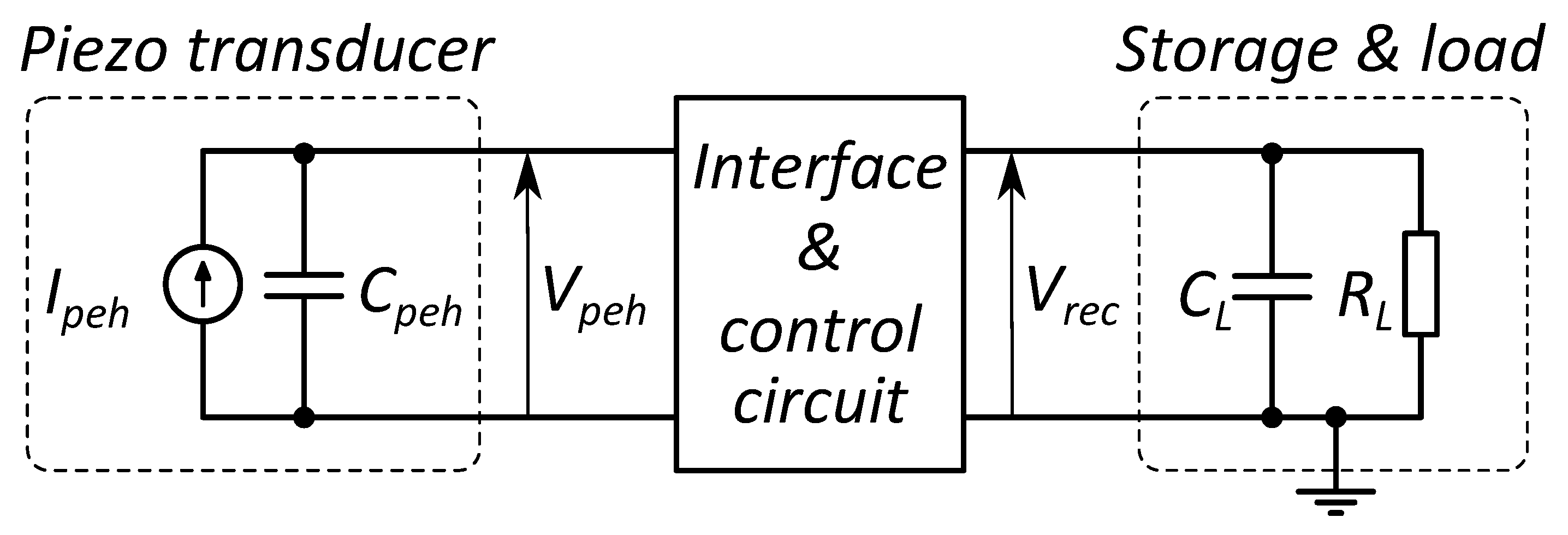
Figure 1 shows the basic topology of a PEH system. It breaks down into three core parts: (1) A piezoelectric transducer (PT). (2) An interface and control circuit (IC). (3) Storage and load elements.
Thanks to the piezoelectric properties of its material, the PT turns the mechanical energy into electrical energy. The equivalent electrical model of the PT consists in the parallel combination of an AC current source, which provides the current I p e h proportional to mechanical excitation, with an inherent piezoelectric capacitor C p e h . The storage element can be a supercapacitor C L , and the load is usually modelled as a resistor R L . Note that R L may change dynamically according to the power requirements of loads such as sensors or wireless modules for instance. The main role of the interface circuit is to rectify the AC voltage of the PT, V p e h , and provide the system with stable voltage supply. Ideally, the voltage supply should be independent of the load but in practice, a change in the value of R L can strongly affect the power efficiency of the harvester.
The most common interface circuit for rectifying V p e h is a Full-Bridge Rectifier (FBR). Yet, the voltage drop across the rectifying diodes makes the FBR unsuitable for low-voltage PT (i.e., V p e h in the 1 V range or below). In order to circumvent the diodes’ threshold issue, Herbawi et al. [8] proposed the principle of active rectification that uses a negative voltage converter (NVC) combined to a series-connected active diode (AD) instead of the FBR Peters et al. [9]. The NVC acts like an FBR but uses transistors instead of diodes, thus yielding lower voltage drop across the rectifier. The AD prevents C L -to-PT current backflow.
Furthermore, the combination of the inherent capacitor C p e h in parallel with I p e h causes I p e h and V p e h to be normally in phase quadrature. This contributes to further dramatically hamper FBR efficiency because C p e h needs to discharge and recharge at each zero-crossing moment of I p e h . Numerous interface topologies and architectures have been proposed to improve power efficiency by applying nonlinear synchronous switching Richard et al. [10]. All these architectures use external devices, i.e.inductor and/or capacitor, to handle the charge of C p e h . Synchronous Electric Charge Extraction (SECE) consists in extracting the energy accumulated in C p e h by transferring it into an inductor, which in turn transfers it into the storage device Hehn et al. [11], Dini et al. [12], Shi et al. [13], Morel et al. [14,15]. SECE alleviates the load dependency of the system but requires a bulky inductor and tends to have degraded performance for periodic excitation of PT. Synchronized Switch Harvesting architectures reuse the own charge of C p e h to invert the polarity of V p e h upon I p e h zero-crossing. They employ either an inductor (SSHI) (Sanchez et al. [4], Du et al. [16], Ramadass and Chandrakasan [17], Wu et al. [18], Chamanian et al. [19,20]) or a set of capacitors (SSHC) (Chen et al. [2], Du and Seshia [3], Chen et al. [21], Hong et al. [22]) to store the charge of C p e h temporarily before sending it back once the electrodes of the PT have been swapped. Architectures combining both an inductor and a capacitor have also been reported in Çiftci et al. [23] and Çiftci et al. [1]. Synchronized-switch-based architectures globally achieve better power efficiency than SECE for both shock and periodic excitation. According to Ramadass and Chandrakasan [17], full voltage flip of V p e h could theoretically allow very high (i.e., infinite) efficiency. Yet, in practice the characteristics of the components strongly limit the voltage flip efficiency, and I p e h still needs to provide C p e h with complementary charge prior to transferring energy from the PT to C L and R L . Moreover, SSHC and SSHI architectures have load-dependent performance, which means that the power efficiency strongly depends on changes in R L and/or the excitation’s amplitude. Çiftci et al. [1] proposed a circuit that reduces the load-dependency of the power efficiency. But such systems require more complex control.
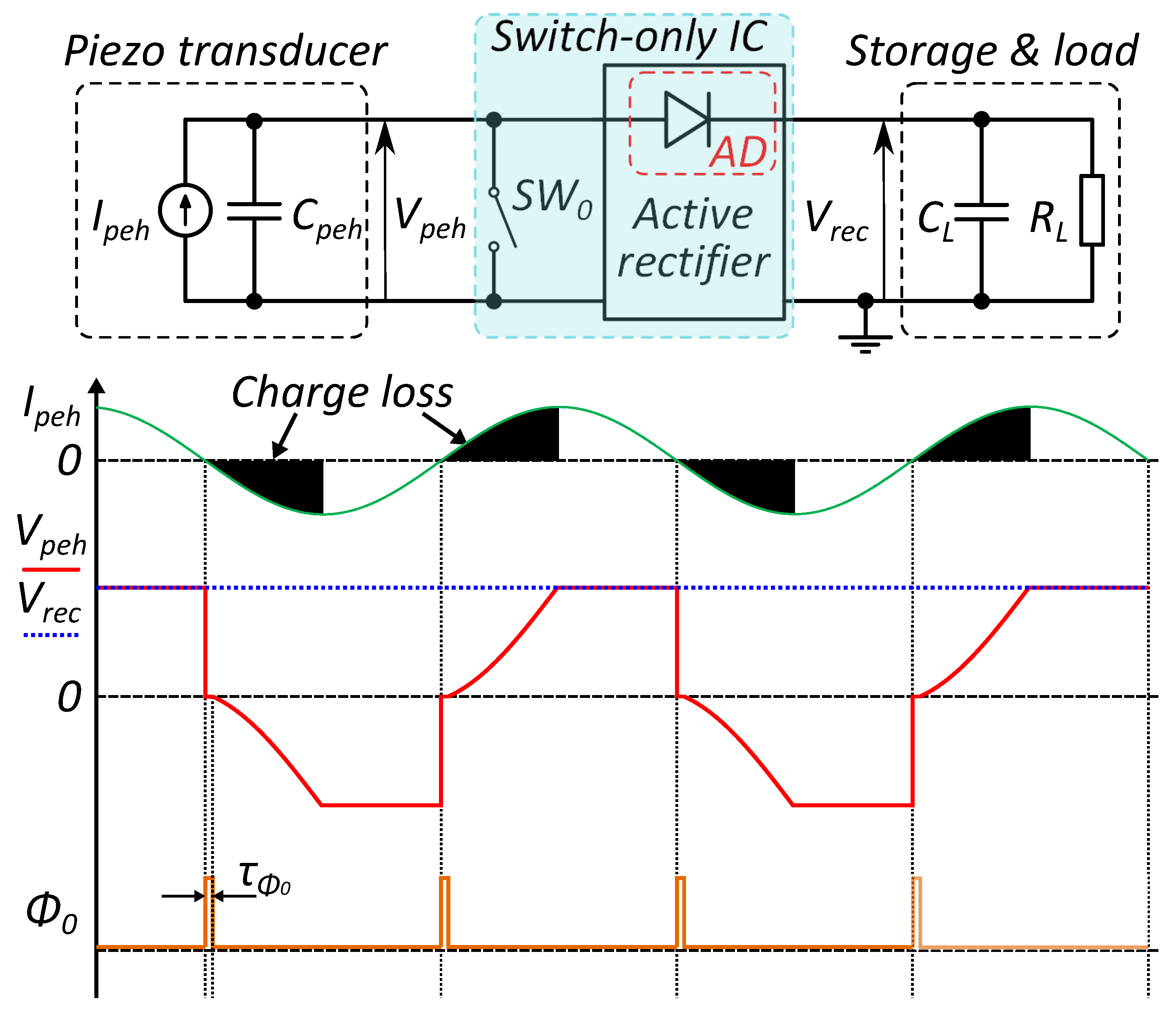
Therefore, there is a genuine interest in proposing an easy-to-implement synchronized switch architecture that both achieves high-efficiency voltage flip and is able to maintain fair power efficiency during transient changes of the load R L . Enhancing the voltage flip minimizes the charge needed by C p e h and thus allows to extract energy from the PT shortly after the voltage flip. This point is particularly critical in low-voltage systems, i.e., V p e h 1 V, that harvest power in the tens of microwatts range.
In this paper, we demonstrate the benefit of a synchronized-switch-based architecture, referred to as full active rectifier (FAR) and first proposed in Wassouf et al. [24], to alleviate the load influence of the piezoelectric energy harvester. The FAR is based on the SSHC concept that consists in flipping V p e h by means of a capacitor, but has much simpler control and needs no additional capacitors. In terms of power performance, the FAR is similar to the Switch-only principle Ramadass [25], and thus performs worse than state-of-the-art SSHI or SSHC. But it is important to note that, discussing raw absolute performance is not the point of this paper. The key result we propose here is the theoretical and experimental proof that thanks to the voltage flip enhancement, the FAR achieves better power efficiency under load constraint than Switch-only. It is yet also important to note that the proposed technique may be applied in addition to state-of-the-art voltage flip architectures that reuse the charge of C p e h (i.e., SSHI and SSHC), and hence contribute to enhance their performance.
The paper is organized as follows: Section 2 presents the enhanced voltage flip concept, the FAR IC topology, its operation principle, and provides a thorough analysis of charge loss and power performance compared to Switch-only. Section 3 provides experimental results. Finally, Section 4 concludes this paper.

2. Enhanced Voltage Flip

The voltage flip enhancement technique that we propose consists in recharging C p e h with C L . At first glance, the concept of reusing the stored charge may appear as counter intuitive but in this section, we demonstrate that it contributes to enhance the power efficiency of the harvester. At each zero-crossing instant of I p e h , the piezo capacitor C p e h is first shorted, and then immediately recharged with a fraction of the charge from the storage capacitor C L Wassouf et al. [24]. In the following sections, the proposed concept will be referred to as the FAR.
The concept is based on the use of a large storage capacitance C L , which should be at least one order of magnitude greater than C p e h . This can easily be admitted because storage capacitances have usually large values. As discussed in Section 2.3, the concept also imperatively needs the rectified voltage V r e c to be regulated, in order to ensure optimal power extraction of the proposed harvester.
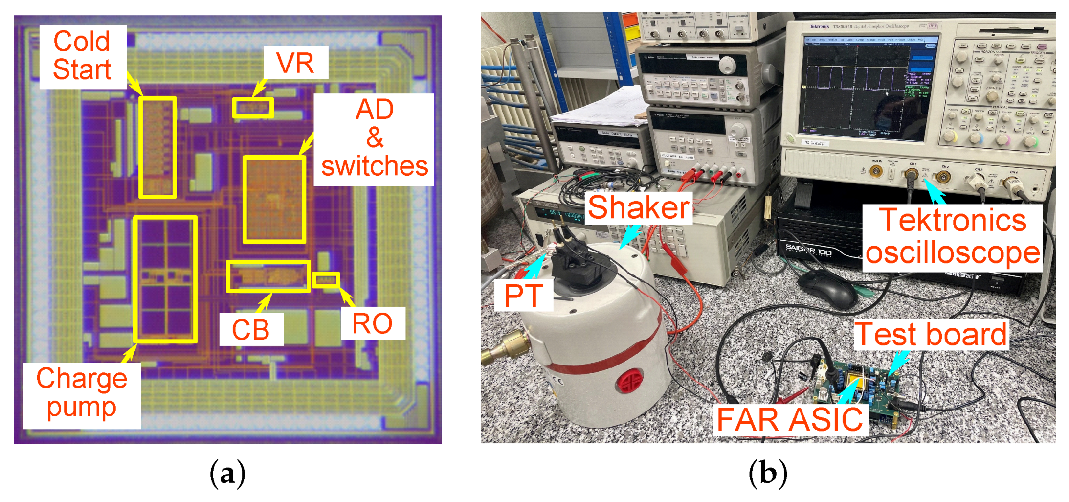
For comparison purpose, because the FAR and the conventional Switch-only principle have a priori the same energy balance, we designed the FAR integrated circuit architecture presented below. This circuit allows to implement both FAR and Switch-only modes.

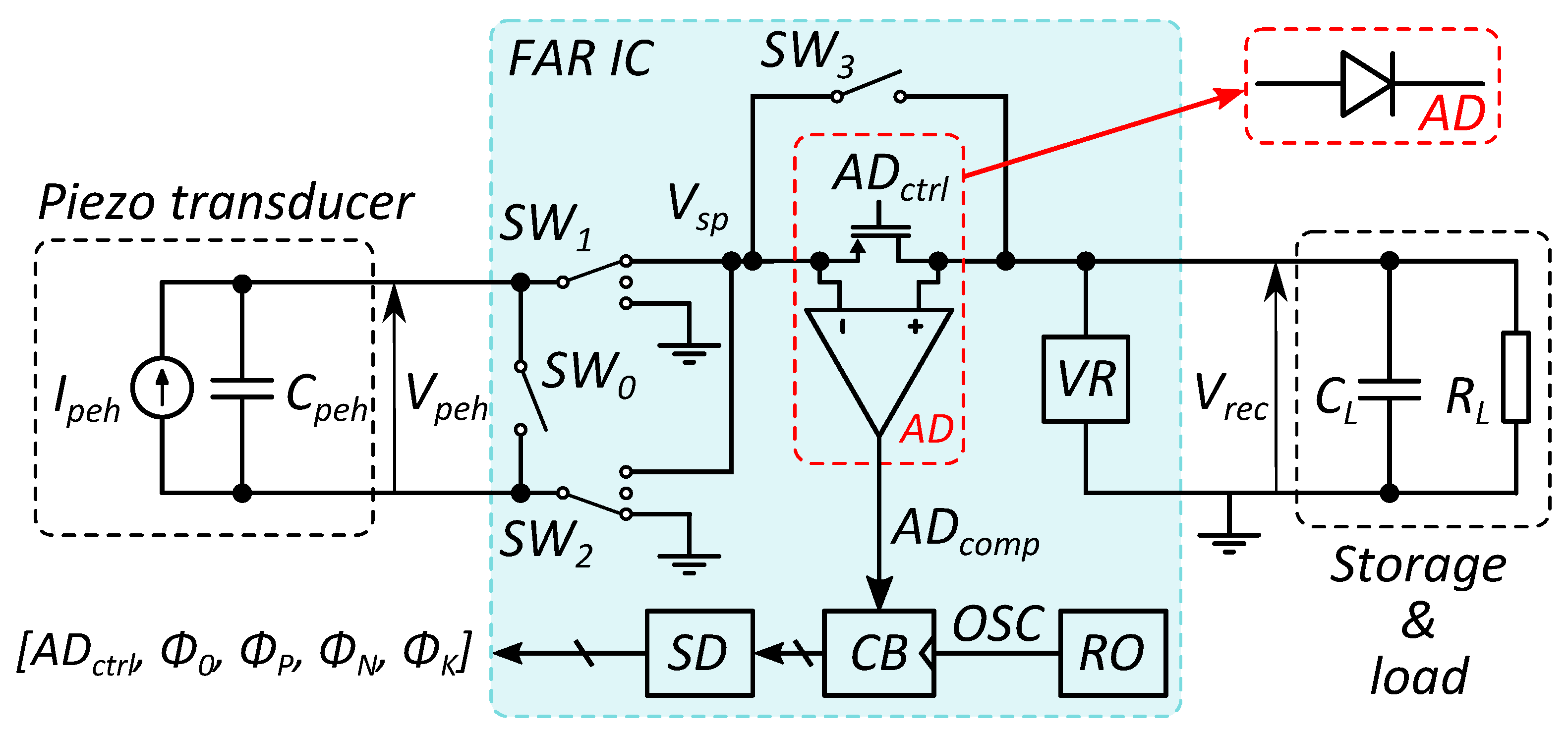
2.1. FAR IC Topology

Figure 2 presents the topology of the FAR IC. A set of switches ( S W 0 to S W 3 ) consisting of transmission gates (TG) is connected to an active diode (AD) to form the rectifying part of the system. The logic control block (CB) of Figure 3 performs the switching sequence described below. The circuit also features a voltage regulator (VR) Du and Seshia [3], a ring oscillator (RO) Ferreira and Galup-Montoro [26], and switch drivers (SD). The later include a charge pump Tsuji et al. [27] and level shifters Du and Seshia [3], Matsuzuka et al. [28] that are needed to control the switches properly. Note that blocks VR, RO and SD are standard functions, which are largely documented in the state-of-the-art literature. Therefore, they are not further detailed in this paper.
The AD is used for both preventing the current from flowing back from C L and detecting the zero-crossing moment of I p e h . It comprises a PMOS switch and an ultra-low power comparator proposed in Du and Seshia [3]. When the voltage at node V s p drops below the rectified output voltage V r e c (Figure 2), the PMOS switch of AD is turned off, and the voltage flip operation is triggered as explained below.

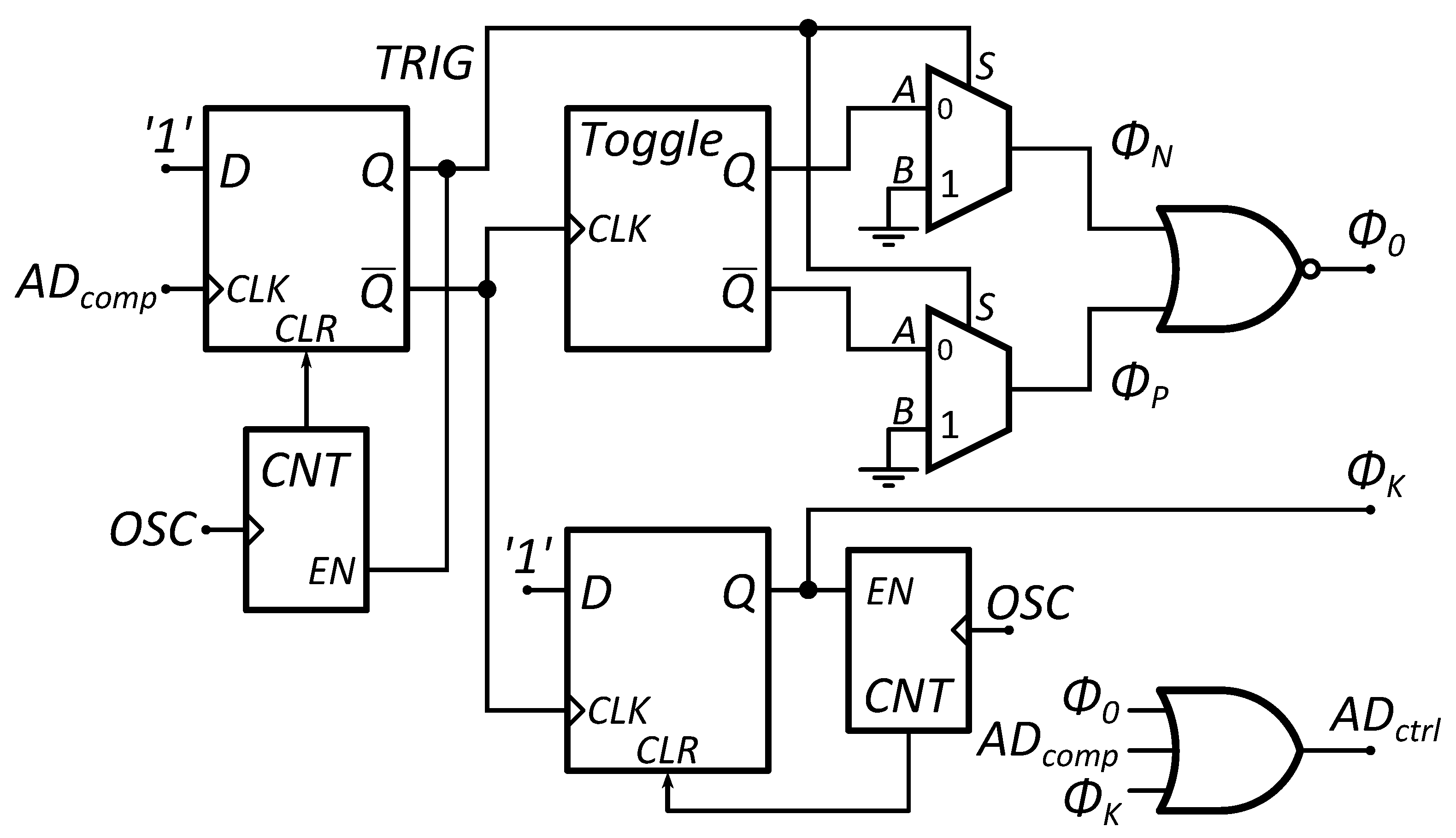
2.2. FAR Operation Principle

The zero-crossing of I p e h causes the AD’s comparator output signal A D c o m p to go high. A D c o m p triggers the signal sequence generated by CB. The CB signals control in turn the AD and the switches S W 0 to S W 3 .
Figure 3 shows the architecture of CB. Signal A D c t r l controls the PMOS switch of AD, signal Φ 0 controls S W 0 , signals Φ P and Φ N both control switches S W 1 and S W 2 , and signal Φ K controls S W 3 . 
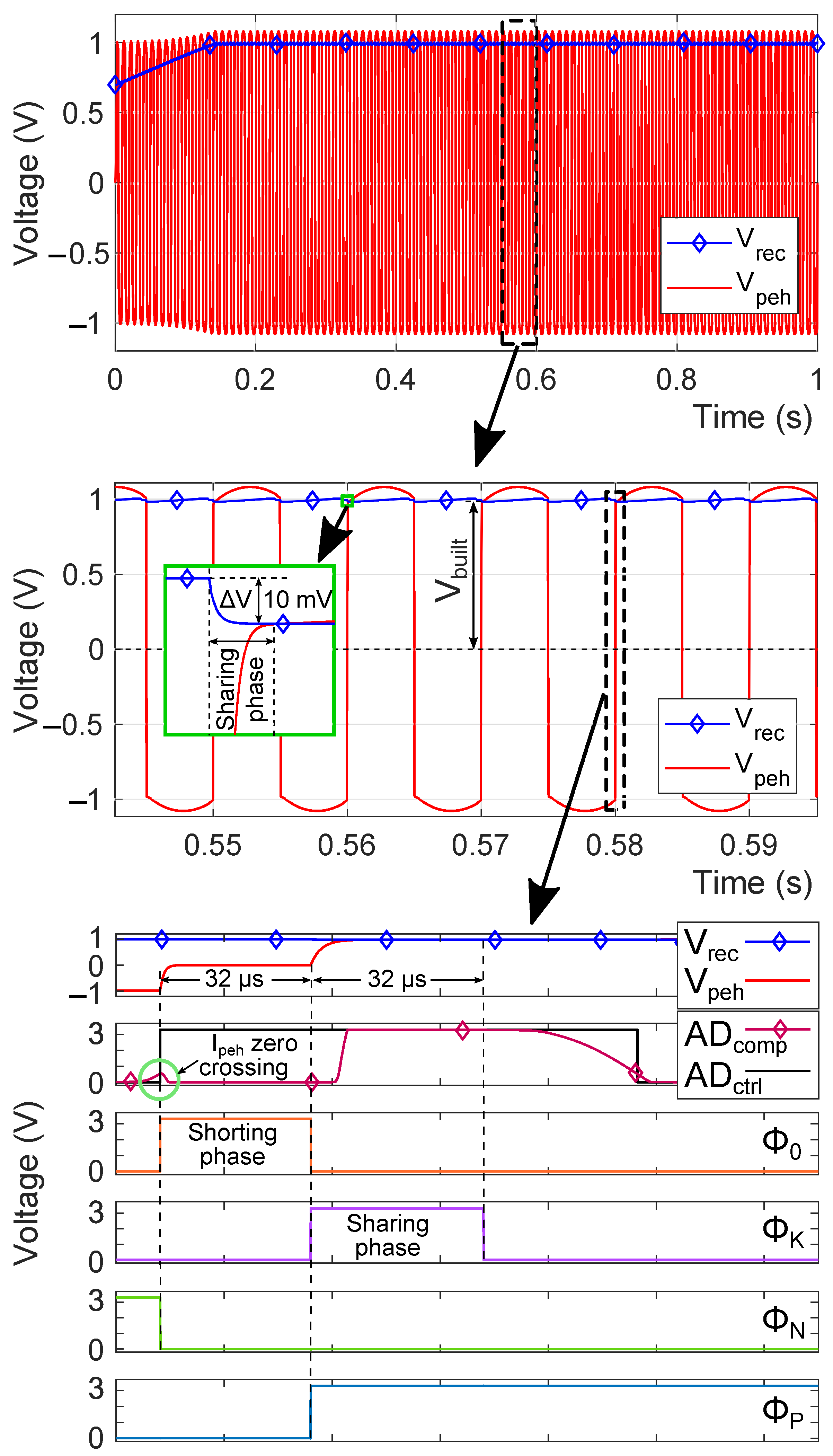
Figure 4 shows the sequence and its effect on the PEH’s voltages, while Table 1 shows the operating scheme of the switches according to the control signals. It is worth noticing that the voltage flip operation is triggered by signal A D c t r l and thus the control block auto-adapts according to the zero-crossing moment of I p e h regardless of the PT’s excitation frequency f e x .
The operation of the FAR breaks down into 3 phases.

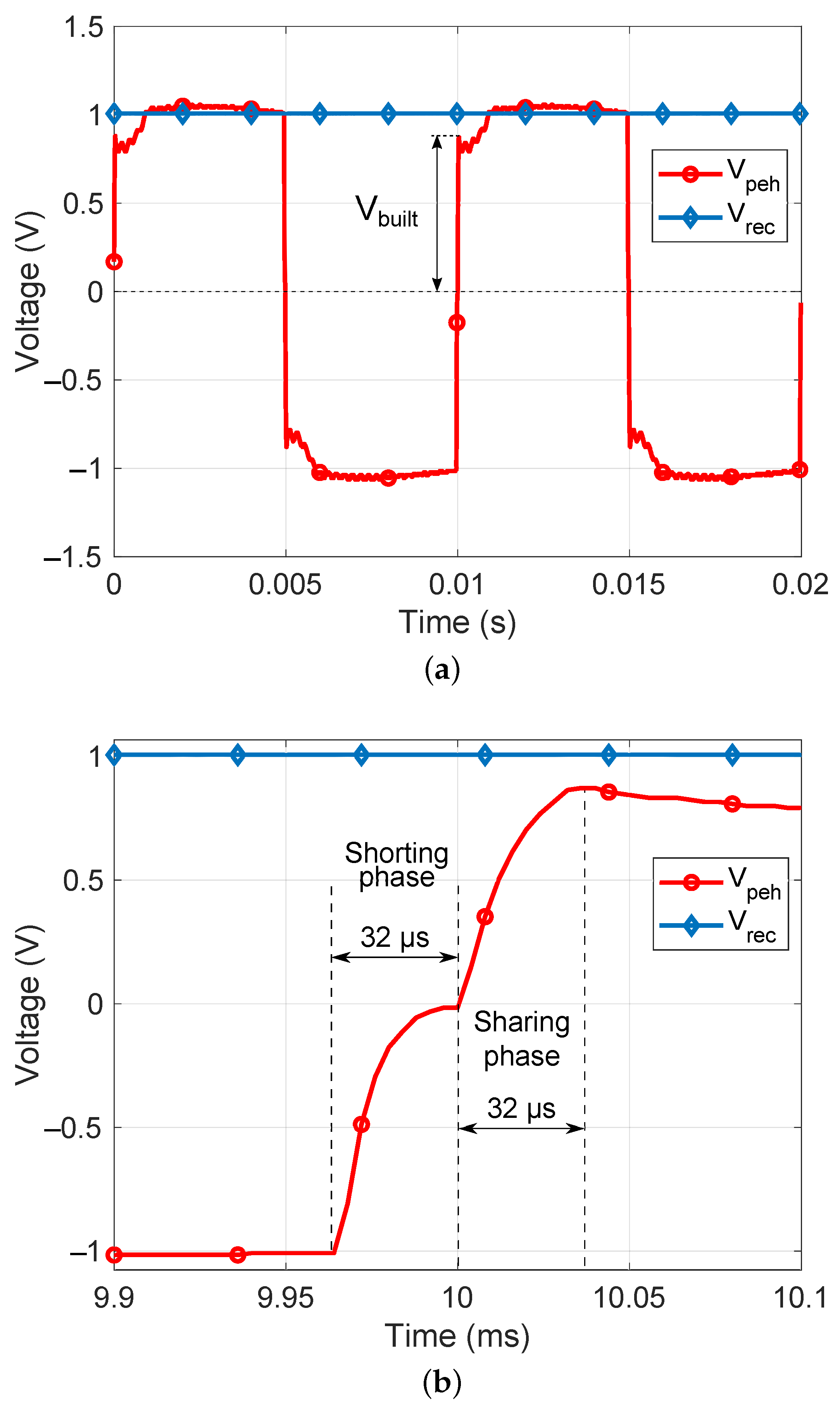
2.2.1. Shorting Phase

Signal A D c o m p acts as the clock signal of a D flip-flop whose data input is set to a constant logic “high” state (Figure 3). When A D c o m p goes high, a trigger signal T R I G turns on signals Φ P and Φ N simultaneously, which puts switches S W 1 and S W 2 in high impedance, i.e., off (Table 1). In the meantime, signal Φ 0 turns on S W 0 (Figure 4), which shorts C p e h . Signal T R I G remains high until C p e h is discharged. The duration of the shorting phase τ Φ 0 depends on the value of C p e h and the resistance of S W 0 . The TGs used to implement the switches have very low ON-resistance, typically around 15 Ω . Assuming C p e h = 100 nF, based on the off-the-shelf transducer characteristics (S118-J12S-1808YB, Piezo.com, accessed on 1 September 2021) used in the experiments (Section 3), the corresponding R C time constant is thus 1.5 µs. The duration τ Φ 0 is controlled by means of a counter (CNT in Figure 3) clocked by the RO signal O S C . This signal is initially used to clock the charge pump used in the switch drivers, and has a frequency of 125 kHz. Therefore, O S C allows controlling τ Φ 0 with 8 µs accuracy. In the proposed system, we used a modulo 4 counter, which thus yields τ Φ 0 = 32 µs. This duration is largely sufficient to ensure complete discharging of C p e h .

2.2.2. Sharing Phase

Once T R I G is reset, i.e., T R I G ¯ goes high, a toggle sets either Φ P or Φ N to high depending on whether I p e h is positive or negative, respectively. When Φ P is high, S W 1 is connected to node V s p and S W 2 is connected to ground, and inversely when Φ N is high (Table 1). In the meantime, Φ K goes high, which closes S W 3 and causes C L to share its charge with C p e h . During this sharing phase, S W 3 is in series with either S W 1 or S W 2 . Since all switches are implemented with the same TGs, the RC time constant is thus 3 µs. Therefore, we also used a modulo 4 counter (Figure 3) to set the duration of the sharing phase τ Φ K = 32 µs, which is also sufficient to complete the charge transfer.
At the end of the sharing phase, the value of V p e h across C p e h is V b u i l t :
V b u i l t = Q L + Q p e h C L + C p e h
V b u i l t only depends on the charge Q L stored in C L , the charge of C p e h being Q p e h = 0 after the shorting phase. If C L C p e h , then V b u i l t   = V r e c V r e c m a x , which is the value of V r e c right before the voltage flip operation is triggered (see Figure 4). Note that, V b u i l t continuously increases as C L charges.

2.2.3. Power Extraction Phase

Once C p e h is recharged, S W 3 turns off while either S W 1 or S W 2 remains on, depending on whether I p e h is negative ( Φ N high) or positive ( Φ P high), respectively (Figure 4). Since the terminals of the PT are swapped by S W 1 and S W 2 at each phase inversion of I p e h , this procudes the rectifying of V p e h (i.e., V s p =   V p e h ). In this phase, the AD’s PMOS switch turns on as soon as V p e h   > V r e c , which in turn connects the PT to C L . As a result, most of the charges transfer directly from PT to C L and R L .
Note that the PMOS switch turns on very shortly after the sharing phase, since the voltage at node V s p is V p e h   =   V b u i l t   = V r e c as mentioned in Section 2.2.2. This has significant consequence on the power efficiency as discussed in Section 2.3.

2.3. Power Performance Analysis

If we suppose that I p e h is a sine current source such as
I p e h t   = I ^ p e h · sin 2 π f e x t
where I ^ p e h represents the amplitude and f e x is the vibration frequency, then the expression of the open-circuit voltage V O C across the PT is given by:
V O C t   = V ^ O C · sin 2 π f e x t + π 4   = 1 C p e h I p e h t d t
with V ^ O C the open-circuit amplitude. When V O C t shifts from V ^ O C to + V ^ O C , the total amount of charge generated by the PT in half a period is thus (Du and Seshia [3], Ramadass [25]):
Q p e h = 2 C p e h V ^ O C = 0 1 / 2 f e x I p e h t d t = 2 I ^ p e h ω
where ω = 2 π f e x .

2.3.1. With Infinite R L

The total charge loss Q l o s s breaks down into two main contributions: Q 1 , lost by C L during the recharging of C p e h (sharing phase) and Q 2 , the charge that goes to C p e h during the power extraction phase, i.e., when C p e h is in parallel with C L .
In steady state, when V r e c reaches its maximum value V r e c m a x (Figure 4) imposed by VR, the expressions for Q 1 and Q 2 are
Q 1 = V b u i l t C p e h = Δ V · C L
Q 2 =   V r e c m a x V b u i l t   ·   C p e h = Δ V · C p e h
where Δ V represents the ripple of V r e c caused by the recharging of C p e h . The total charge loss is then
Q l o s s = C p e h ·   Δ V + V b u i l t   = C p e h · V r e c
From (1) and (5), we may consider Δ V 0 provided that C L C p e h . Therefore, we can consider that C L fully recharges C p e h , making Q 1 = V b u i l t · C p e h the principal charge loss (i.e., Q 1 Q l o s s ). We can thus express the total charge stored on C L in half a period as
Q L = Q p e h Q l o s s = C p e h ·   2 V ^ O C V r e c
and then the total charge on a full period is then 2 Q L .
Thus, the output power is given by
P r e c = 2 V r e c f e x Q L = 2 V r e c f e x C p e h ·   2 V ^ O C V r e c
From (9), we can deduce that the maximum power extraction is achieved when V r e c = V ^ O C , which corresponds to a maximum power
P r e c m a x = 2 C p e h V ^ O C 2 f e x
This result shows that the power efficiency is inherently load-dependent because applying a finite value load R L affects V r e c , as it would for any synchronized switch harvesting system ( Çiftci et al. [1], Chen et al. [21], Du et al. [29]) and suggests VR should regulate V r e c to V ^ O C (Ramadass and Chandrakasan [17]). Moreover, it is identical to Switch-only, the architecture and signals of which are presented in Figure 5.
When R L is infinite and V r e c is regulated to V ^ O C , the amount of charge needed to recharge either C L (FAR) or C p e h (Switch-only) is Q p e h / 2 . Yet, energy harvesting systems are meant to supply a finite value load with charges delivered by C L and PT. As demonstrated in the next section and in Section 3.2, the proposed FAR architecture has an impact on the power performance when R L has finite value. Furthermore, since FAR and Switch-only have the same power performance a priori, we compared both architectures.
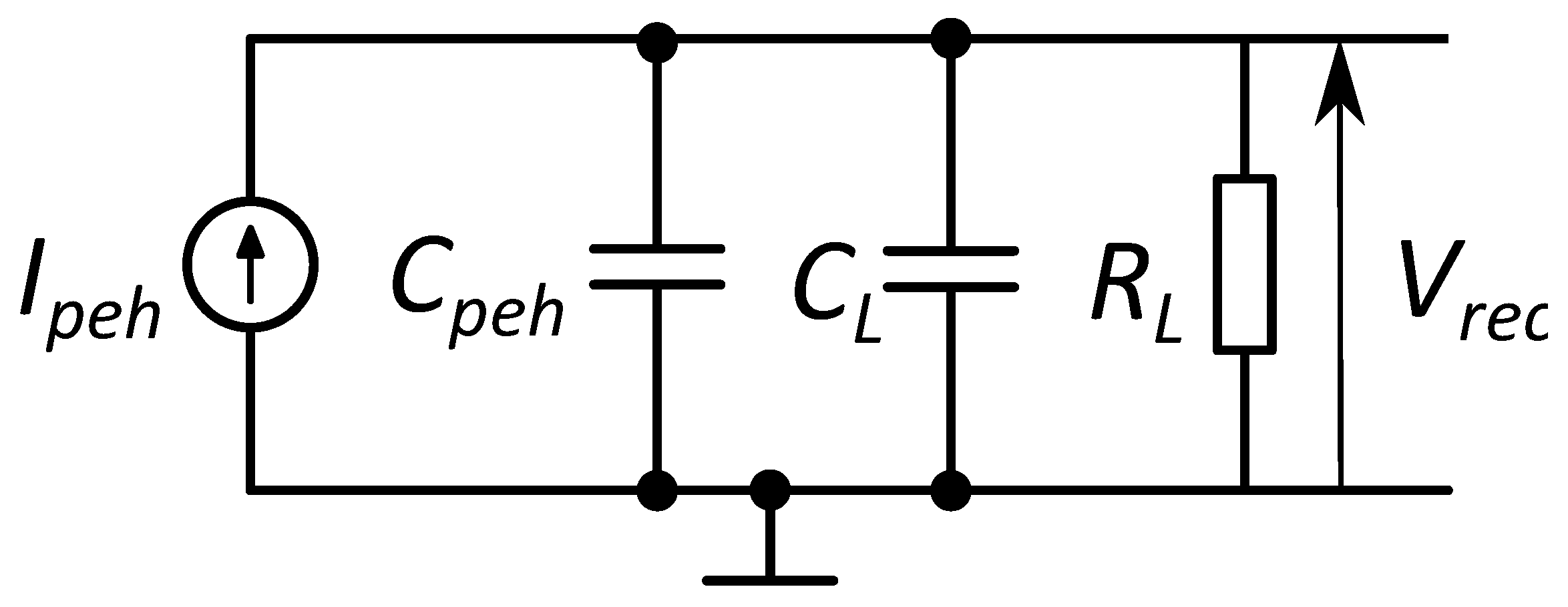
2.3.2. With Finite R L

Figure 6 shows the equivalent electrical model of the PEH during the power extraction phase (i.e., AD is “ON”), when R L has a finite value. Note that this model assumes the series resistances of the switches and ADs are negligible, which is realistic considering R L is around several tens of kilo-ohms as discussed below. The expression of V r e c is given by:
V r e c t   = K e t τ + R L I ^ p e h 1 + τ ω 2 sin ω t     R L τ ω I ^ p e h 1 + τ ω 2 cos ω t
where τ = R L C / / and K is the initial condition constant such as V r e c 0   = V b u i l t , considering t = 0 s corresponds to the zero-crossing moment of I p e h . Equation (11) applies for V r e c lower than V ^ O C . When V r e c reaches V ^ O C , it is regulated to this value by VR.
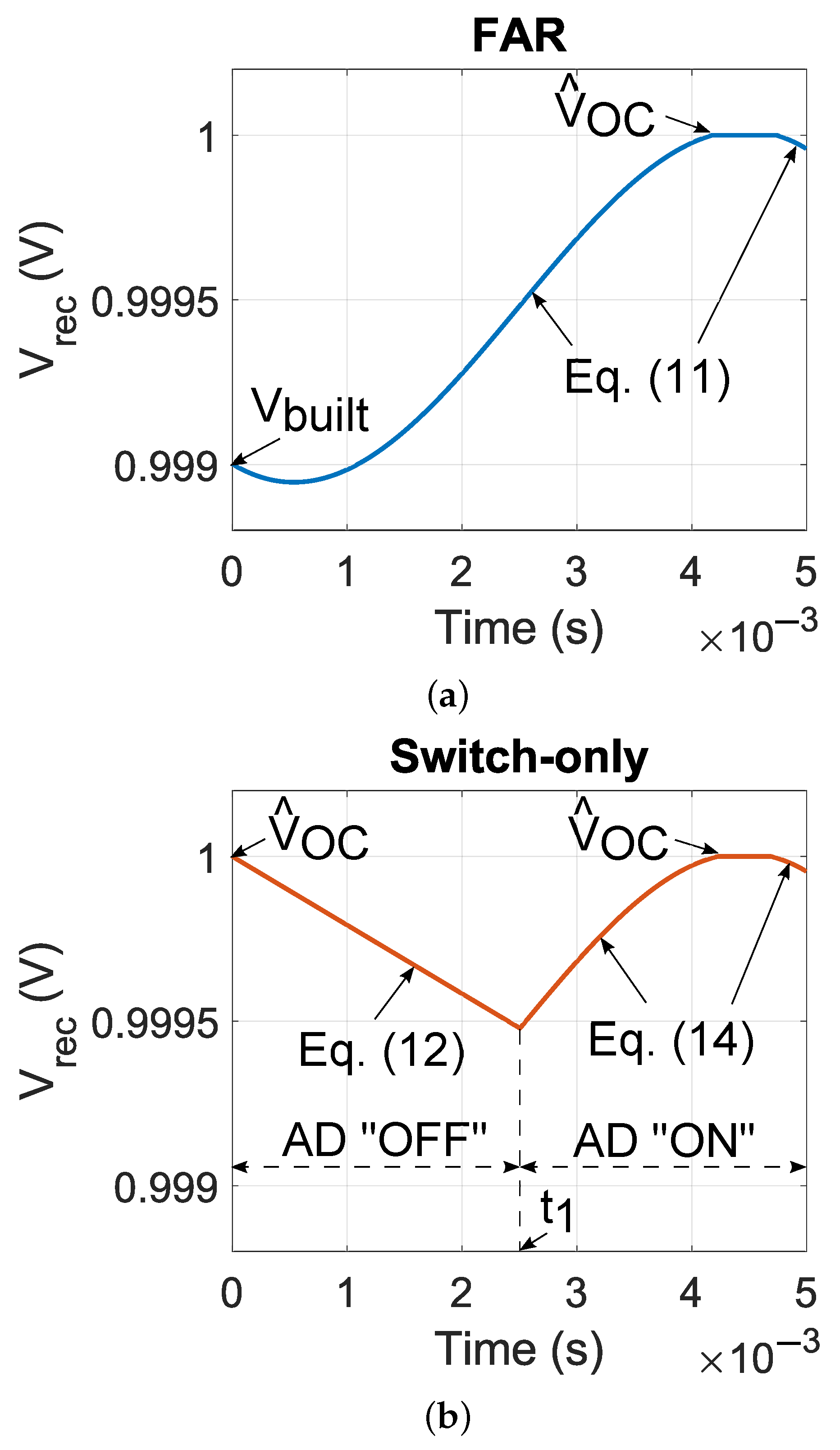
 Figure 7a shows V r e c t for the FAR architecture ( V r e c F A R ) simulated on half a period of I p e h when applying a finite load R L at t = 0 s. The parameters of PT are: C p e h = 100 nF and I p e h = 20 π e 6 A, and the excitation frequency is f e x = 100 Hz. This corresponds to V ^ O C = 1 V. The load is R L = 48 k Ω , and K is set so that V r e c 0   = K R L τ ω I ^ p e h / 1 + τ ω 2   = V ^ O C · C L / C p e h + C L , which is the value of V b u i l t when V r e c = V ^ O C at the zero-crossing moment of I p e h (See Section 2.2.2).
In the Switch-only architecture, the evolution of V r e c breaks down into two phases. First, its AD is “OFF” and C p e h recharges, while in the meantime, C L discharges into R L . Therefore, in this phase, V r e c and V p e h evolve separately. On the one hand, the expression of V r e c is
V r e c t   = K S O e t R L C L
where K S O is the initial value of V r e c at the zero-crossing moment of I p e h . On the other hand, the expression of V p e h is
V p e h t   = V ^ O C V ^ O C · cos ω t
The second phase of V r e c for the Switch-only starts when AD is “ON” (i.e., V p e h   = V r e c ). In this phase, the equivalent schematic of the Switch-only architecture is exactly the same as for the FAR (cf. Figure 6). Therefore, the expression of V r e c is deduced from (11) but with an offset V o f f :
V r e c t   = K e t τ + R L I ^ p e h 1 + τ ω 2 sin ω t     R L τ ω I ^ p e h 1 + τ ω 2 cos ω t   +   V o f f
This offset V o f f is induced by the decay of V r e c during the first phase of Switch-only. Furthermore, just as for the FAR architecture, when V r e c reaches V ^ O C , it is regulated by VR. Figure 7b shows V r e c for the Switch-only architecture ( V r e c S O ) simulated with the same parameters as for the FAR simulation presented in Figure 7a. Note that, for Switch-only V r e c 0   = K S O = V ^ O C = 1 V.
To establish whether V o f f is positive or negative, i.e., which one yields the greater value (11 or 14, FAR or Switch-only), we first needed to find the moment t 1 when V r e c of Switch-only caught up with V p e h , which corresponds to the moment when AD turns “ON”:
K S O e t 1 R L C L = V ^ O C V ^ O C · cos ω t 1
Note: there is no analytic expression to solve (15). Therefore, to evaluate t 1 we need to apply a numerical method, such as Newton–Raphson ( Conejo and Baringo [30]). The value t 1 is then injected into (14) to determine V o f f so that Equations (12)–(14) yield the same value. Numerical simulations (Figure 8) reveal that, whatever the values of the parameters in (11) and (14), V o f f < 0 , which means that for t t 1 , V r e c F A R > V r e c S O .
This result has significant consequences for the power efficiency of the systems as R L evolves. More specifically, from (11) we found the limit value R L lim of R L for which V r e c F A R reached V ^ O C at t = T / 2 . Applying R L l i m in (14) yielded V r e c S O T / 2 < V ^ O C . Since the value of V r e c T / 2 set the initial conditions of V r e c for the next half period of I p e h , we verified that for R L = R L lim , the average value of V r e c S O decreased to compensate for the presence of R L while the average value of V r e c F A R remained constant. More generally, when R L < R L lim , V r e c decreased in both architectures, V r e c S O decreased faster and, more importantly, stabilized to a lower value than V r e c F A R . Note that, for either architecture, V r e c adjusted to a steady-state average value that depended on the amount of energy the harvester transfered from the PT to R L . This amount was lower in Switch-only because the power extraction phase was shorter than in FAR. Furthermore, the value of C L only affected the evolution speed of V r e c when R L changed. The faster decreasing speed of V r e c S O cames from the smaller time constant R L C L when the ADwas “OFF” (see 12). The same reason explains why V r e c S O stabilized at a lower value than V r e c F A R . 
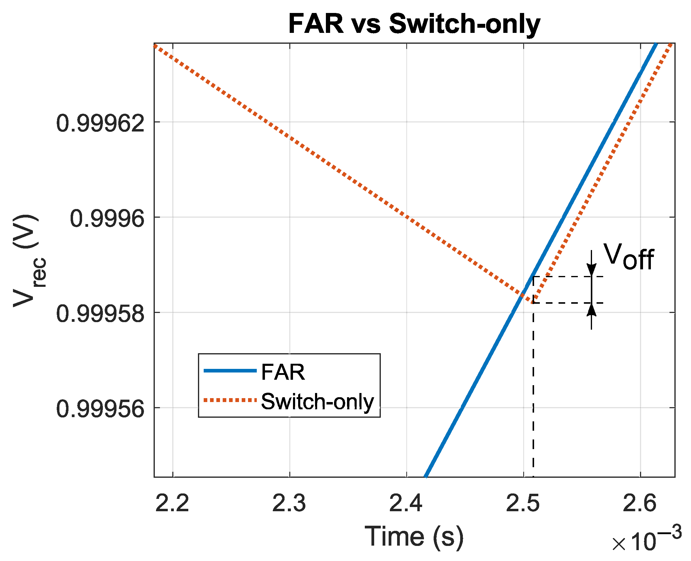
Figure 9 shows the numerical simulations of both architectures with R L = 48 k Ω and the same initial conditions as above. We noticed that V r e c S O stabilized around 3 mV below V r e c F A R .
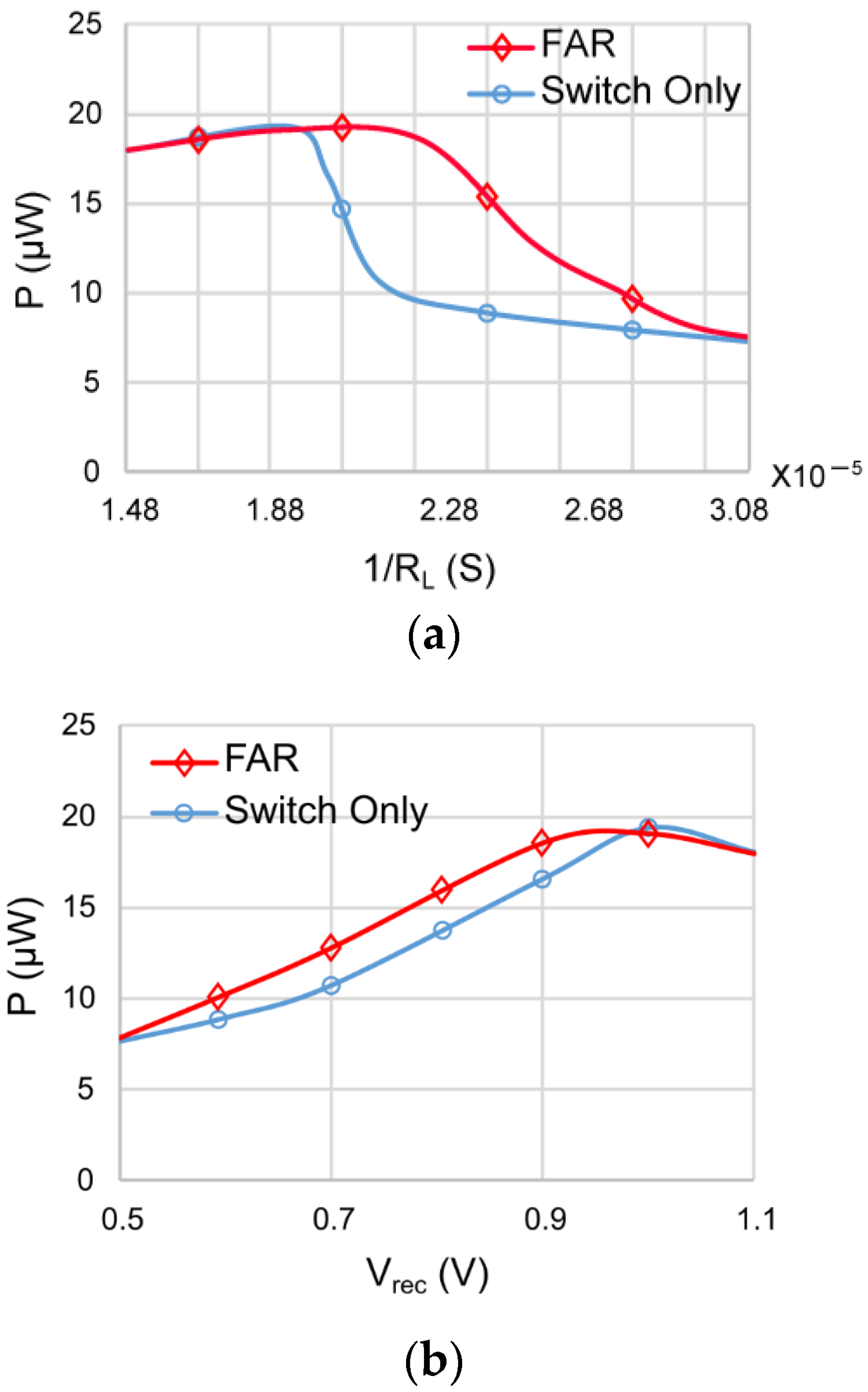
For power, FAR was also more efficient than Switch-only once V r e c had been stabilized. 
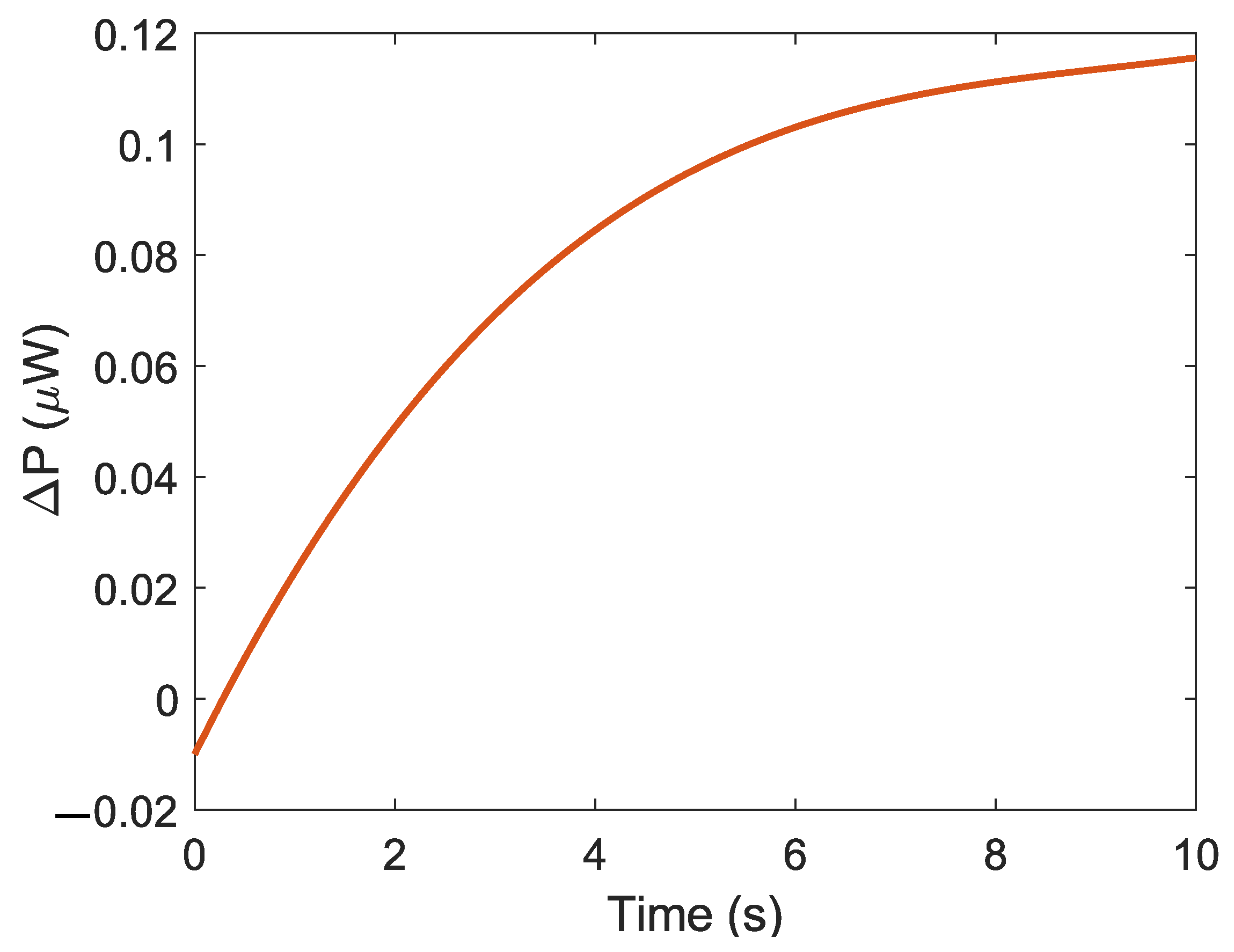
Figure 10 shows the average power difference Δ P = P F A R P S O between FAR and Switch-only. It is worth noticing that at t = 0 s, i.e., before and shortly after applying R L , Switch-only achieved slightly better power performance than FAR ( Δ P < 0 ). This was due to the fact that without R L , the FAR principle yielded lower average values of V r e c . However, energy harvesting systems are not just meant to charge a storage device; they are intrinsically designed to supply energy to a load. Therefore, as shown here in the FAR implementation, there was a benefit in using voltage flip enhancement to improve power performance.
Furthermore, we believe that combining the voltage flip enhancement principle to SSHI or SSHC might contribute to further improve the power performance under load constraint. But for the time being, this statement is based on theoretical assumptions and needs to be further investigated.

3. Experimental Results and Discussion

3.1. Prototype Design and Experimental Setup

We designed and tested a fully integrated prototype fabricated using AMS 0.35 µm High-Voltage CMOS technology. The circuit features all the blocks of the FAR architecture presented in Figure 2. The voltage supply was 3.3 V for AD, SD and VR and 1.2 V for CB and RO (Figure 2). Note that CB can be configured either in FAR or in Switch-only mode to allow performance comparison between both architectures.
To validate the voltage flip efficiency, we performed post-layout transistor-level 1 s transient simulations with C L = 10 µF and no load resistance R L . The model of the PT was based on the off-the-shelf device S118-J12S-1808YB by Piezo.com (accessed on 1 September 2021) with C p e h = 100 nF. We set I ^ p e h and f e x to achieve an open-circuit amplitude V ^ O C = 1 V. According to (3), this corresponds to I ^ p e h = 20 π e 6 A 62.8 µA and f e x = 100 Hz. Since there was no R L , we set VR to regulate V r e c to V ^ O C , which corresponded to the theoretical maximum power efficiency, P r e c m a x = 20 µW according to (10).
Figure 11 shows the simulation results performed with Cadence®. Note that C L was pre-charged with V r e c = 0.7 V by a cold start circuit, not detailed here. Once V r e c 0.7 V, the control block CB was activated and the the FAR system started to operate. The middle plot in Figure 11 shows that when V r e c was regulated to V ^ O C , V b u i l t was around 0.99 V ( Δ V 10 mV, see inset zoom view), which corresponded to 99% voltage flip efficiency. It also revealed the effect of the “ON” resistance of the non-ideal AD PMOS switch, which caused V p e h   = V s p to exceed V r e c . The bottom plot focusedon a voltage flip sequence following a zero-crossing of I p e h . The voltage flip duration was 64 µs. One noticed that the AD output signal A D c o m p returned to a low level almost instantly after the voltage flip operation started. This was due to a temporary increase in voltage at node V s p (Figure 2) caused by charge injection when switches S W 1 and S W 2 opened. Therefore, to prevent spurious behavior of the FAR, the signal A D c t r l was locked by the combinatorial O R function of A D c o m p , Φ 0 and Φ K . Signal A D c o m p went high again as C p e h recharged during the sharing phase, and eventually returned to low leveld shortly after this phase was complete, as V p e h   = V s p increased and power extraction started.
Figure 12 shows a micrograph of the ASIC and the test bench. For mechanical excitation, we used an LDS® V400 series shaker by Brüel & Kjær, driven by an AC power source 6813B by Agilent®. The excitation signal was a 100 Hz sine waveform and the acceleration was set to get V ^ O C = 1 V. For these experiments, the extracted energy was stored on a conventional capacitor C L = 100 µF. A LabVIEW® platform performs shaker control and raw signal acquisition via a Tektronix® TDS series digital oscilloscope.

3.2. Experimental Results

Figure 13 shows the measured waveforms of V p e h and V r e c corresponding to the above mentioned parameters and operating conditions of the FAR architecture. After the voltage flip operation, the voltage across C p e h was V b u i l t = 0.864 V. This corresponded to 86.4% voltage flip efficiency, which was lower than the Cadence simulated value. There were two reasons for this. First, when operating the PT close to its mechanical resonance frequency (130 Hz), the strong coupling effect induced harmonic oscillations that prevented complete voltage flip, as can be seen in Figure 13a. Second, the series resistance of the T-gate switches combined with the various interconnections between the test board and the PT induced a larger time constant. As can be seen on Figure 13b, this effect was greater during the sharing phase when the charge from C L transited through S W 3 and S W 2 / 3 , and the series resistance was thus larger than during the shorting phase. One solution to circumvent this issue was to extend the duration of the sharing phase, but this had only limited benefit because the deleterious effect of harmonic oscillations prevailed. We experimentally determined that a 32 µs sharing phase duration yielded optimal voltage flip efficiency.
Note that with C L = 100 µF, the voltage ripple Δ V on V r e c is negligible (i.e., below 1 mV).
To evaluate the benefit of the proposed voltage flip enhancement principle on power efficiency, we measured the output power in both FAR and Switch-only mode. For this experiment, we applied a variable load resistance and disabled VR. Figure 14a shows the output power as a function of 1 / R L . One can clearly see that FAR achieved better power performance as 1 / R L increased and delivered around 100% more power than Switch-only for 1 / R L 0.024 S ( R L 41 k Ω ). Yet, as demonstrated in Section 2.3.2 (see Figure 9), for a given value of R L , both architectures did not yield the same output voltage. Therefore, for a more realistic comparison, Figure 14b shows the output power as a function of V r e c . For both architectures maximum power was achieved when V r e c V ^ O C . As mentioned in Section 2.3.2, Switch-only achieved slightly better performance than FAR with P S O m a x = 19.3 µW and P F A R m a x = 19.1 µW, respectively. Yet, for a given value of V r e c < V ^ O C , FAR delivered up to 20% more power than Switch-only. This result confirmed the theoretical demonstration (Section 2.3.2) that FAR achieved better power efficiency than Switch-only under load constraint. It is also worth pointing out that FAR kept operating, and the efficiency improvement ratio remained almost constant (around 20%), for V r e c as low as 0.7 V, i.e., as the load constraint increased (when R L drained more current from C L ). Note that for V r e c < 0.5 V, the ASIC was unable to work properly.
Concerning absolute value, the measurements revealed that the power improvement of FAR over Switch-only was much more significant than the simulations presented in Figure 9 and Figure 10. The reason is that FAR was more robust against circuit non-idealities than Switch-only, and particularly against the offset of the AD comparator, which can be as high as a few millivolts. Indeed, in FAR, during the sharing phase S W 3 shorted the inputs of the AD comparator and the voltage at node V s p was pre-charged to V r e c . This caused the comparator to flip state shortly after the sharing phase had been completed, as mentioned in Section 2.2.3. Conversely, in Switch-only V p e h first had to overcome the offset of the AD comparator before power extraction started. The influence of the offset was particularly important for large C L as a few millivolts difference between V r e c and V p e h may represent a large amount of charge and thus a large power difference. For the time being, this was the most tangible assumption, but further investigations are currently under way to gain a better understanding of this phenomenon.
The maximum output power improving rate (MOPIR) (Ramadass and Chandrakasan [17], Chen et al. [21]) allows the comparison of FAR power performance with that of a conventional FBR.
M O P I R = P F A R P F B R
where P F A R and P F B R are the output powers of FAR and FBR, respectively. The maximum output power of FBR is (Ramadass and Chandrakasan [17])
P F B R m a x = C p e h f e x V ^ O C 2 V t h
where V t h is the diodes’ threshold voltage. If we consider a conventional Schottky-diode based FBR with high-performance diodes having a low V t h (around 0.3 V), using a FBR under the same operating condition as the FAR yielded P F B R m a x = 1.6 µW. The MOPIR was thus around 11.94× .
Table 2 compares the proposed FAR concept with some of the best results available in the recent literature. As mentioned in the introduction, discussing absolute raw performance was not the object of this paper. When considering the FAR as a stand-alone rectifier solution, the power efficiency was equivalent to Switch-only, which was much lower than the SSHI or SSHC systems referenced in the table. Hence, the PIC was lower compared to the state-of-the-art. Nevertheless, the FAR operated with an open circuit V O C of only 1 V while the latest systems usually have a larger V O C . Therefore, compared to a conventional diode-based FBR, the output power ratio of FAR was much higher, and above all, helped keep power efficiency as the load constraint increased.

4. Conclusions

This paper reported on a simple concept of voltage flip enhancement for piezoelectric energy harvesting. A thorough analysis of the power performance revealed that, besides the boost effect on the voltage flip, the FAR principle also helped improve the power efficiency of the PEH, especially as the load constraint increased. The FAR can be used as a fully integrated standalone rectifier solution, and is particularly well suited for low-voltage operation. Yet, it may also be considered as an additional boost solution to improve the performance of more a complex PEH architecture such as SSHI or SSHC. Experimental results performed on a CMOS prototype confirmed that, under load constraint, the FAR principle achieved better performance compared to Switch-only, and is more robust against circuit non-idealities. These conclusive results opened interesting research perspectives that we are currently working on, consisting of combining the FAR principle with SSHI or SSHC to improve both voltage flip and power efficiency.

Author Contributions

Conceptualization, V.F., L.W.; methodology, V.F., E.J.; resources, V.F., L.W., E.J.; writing—original draft, V.F.; writing—review and editing, V.F., E.J. All authors have read and agreed to the published version of the manuscript.

Funding

This research was funded by the Agence Nationale de la Recherche: ANR-18-CE09-0033.

Conflicts of Interest

The authors declare no conflict of interest.

References

  1. Çiftci, B.; Chamanian, S.; Koyuncuoğlu, A.; Muhtaroğlu, A.; Külah, H. A Low-Profile Autonomous Interface Circuit for Piezoelectric Micro-Power Generators. IEEE Trans. Circuits Syst. I Regul. Pap. 2021, 68, 1458–1471. [Google Scholar] [CrossRef]
  2. Chen, Z.; Jiang, Y.; Law, M.; Mak, P.; Zeng, X.; Martins, R.P. 27.3 A Piezoelectric Energy-Harvesting Interface Using Split-Phase Flipping-Capacitor Rectifier and Capacitor Reuse Multiple-VCR SC DC-DC Achieving 9.3× Energy-Extraction Improvement. In Proceedings of the 2019 IEEE International Solid-State Circuits Conference–(ISSCC), San Francisco, CA, USA, 17–21 February 2019; pp. 424–426. [Google Scholar] [CrossRef]
  3. Du, S.; Seshia, A.A. An Inductorless Bias-Flip Rectifier for Piezoelectric Energy Harvesting. IEEE J. Solid-State Circuits 2017, 52, 2746–2757. [Google Scholar] [CrossRef] [Green Version]
  4. Sanchez, D.A.; Leicht, J.; Hagedorn, F.; Jodka, E.; Fazel, E.; Manoli, Y. A Parallel-SSHI Rectifier for Piezoelectric Energy Harvesting of Periodic and Shock Excitations. IEEE J. Solid-State Circuits 2016, 51, 2867–2879. [Google Scholar] [CrossRef]
  5. Rahimi, A.; Zorlu, O.; Muhtaroglu, A.; Külah, H. Fully Self-Powered Electromagnetic Energy Harvesting System with Highly Efficient Dual Rail Output. IEEE Sens. J. 2012, 12, 2287–2298. [Google Scholar] [CrossRef]
  6. Tao, K.; Liu, S.W.; Miao, J.M.; Lye, S.W. A three-dimensional electrostatic/electret micro power generator for low acceleration and low frequency vibration energy harvesting. In Proceedings of the 2014 IEEE 27th International Conference on Micro Electro Mechanical Systems (MEMS), San Francisco, CA, USA, 26–30 January 2014; pp. 366–369. [Google Scholar] [CrossRef]
  7. Stanzione, S.; Liempd, C.V.; Nabeto, M.; Yazicioglu, F.R.; Hoof, C.V. 20.8 A 500 nW batteryless integrated electrostatic energy harvester interface based on a DC-DC converter with 60 V maximum input voltage and operating from 1 μW available power, including MPPT and cold start. In Proceedings of the 2015 IEEE International Solid-State Circuits Conference–(ISSCC) Digest of Technical Papers, San Francisco, CA, USA, 22–26 February 2015; pp. 1–3. [Google Scholar] [CrossRef]
  8. Herbawi, A.S.; Velarde, F.; Paul, O.; Galchev, T. Self-powered CMOS active rectifier suitable for low-voltage mechanical energy harvesters. In Proceedings of the 2016 IEEE SENSORS, Orlando, FL, USA, 30 October–3 November 2016; pp. 1–3. [Google Scholar] [CrossRef]
  9. Peters, C.; Handwerker, J.; Maurath, D.; Manoli, Y. A Sub-500 mV Highly Efficient Active Rectifier for Energy Harvesting Applications. IEEE Trans. Circuits Syst. I Regul. Pap. 2011, 58, 1542–1550. [Google Scholar] [CrossRef]
  10. Richard, C.; Guyomar, D.; Audigier, D.; Ching, G. Semi-Passive Damping Using Continuous Switching of a Piezoelectric Device; Symposium on Smart Structures and Materials; International Society for Optics and Photonics: Newport Beach, CA, USA, 1999; pp. 104–111. [Google Scholar] [CrossRef]
  11. Hehn, T.; Hagedorn, F.; Maurath, D.; Marinkovic, D.; Kuehne, I.; Frey, A.; Manoli, Y. A Fully Autonomous Integrated Interface Circuit for Piezoelectric Harvesters. IEEE J. Solid-State Circuits 2012, 47, 2185–2198. [Google Scholar] [CrossRef]
  12. Dini, M.; Romani, A.; Filippi, M.; Tartagni, M. A Nanopower Synchronous Charge Extractor IC for Low-Voltage Piezoelectric Energy Harvesting With Residual Charge Inversion. IEEE Trans. Power Electron. 2016, 31, 1263–1274. [Google Scholar] [CrossRef]
  13. Shi, G.; Xia, Y.; Wang, X.; Qian, L.; Ye, Y.; Li, Q. An Efficient Self-Powered Piezoelectric Energy Harvesting CMOS Interface Circuit Based on Synchronous Charge Extraction Technique. IEEE Trans. Circuits Syst. I Regul. Pap. 2018, 65, 804–817. [Google Scholar] [CrossRef]
  14. Morel, A.; Gasnier, P.; Wanderoild, Y.; Pillonnet, G.; Badel, A. Short Circuit Synchronous Electric Charge Extraction (SC-SECE) Strategy for Wideband Vibration Energy Harvesting. In Proceedings of the 2018 IEEE International Symposium on Circuits and Systems (ISCAS), Florence, Italy, 27–30 May 2018; pp. 1–5. [Google Scholar] [CrossRef] [Green Version]
  15. Morel, A.; Pillonnet, G.; Gasnier, P.; Lefeuvre, E.; Badel, A. Frequency tuning of piezoelectric energy harvesters thanks to a short-circuit synchronous electric charge extraction. Smart Mater. Struct. 2019, 28, 025009. [Google Scholar] [CrossRef] [Green Version]
  16. Du, S.; Amaratunga, G.A.J.; Seshia, A.A. A Cold-Startup SSHI Rectifier for Piezoelectric Energy Harvesters With Increased Open-Circuit Voltage. IEEE Trans. Power Electron. 2019, 34, 263–274. [Google Scholar] [CrossRef]
  17. Ramadass, Y.K.; Chandrakasan, A.P. An Efficient Piezoelectric Energy Harvesting Interface Circuit Using a Bias-Flip Rectifier and Shared Inductor. IEEE J. Solid-State Circuits 2010, 45, 189–204. [Google Scholar] [CrossRef] [Green Version]
  18. Wu, L.; Do, X.; Lee, S.; Ha, D.S. A Self-Powered and Optimal SSHI Circuit Integrated With an Active Rectifier for Piezoelectric Energy Harvesting. IEEE Trans. Circuits Syst. I Regul. Pap. 2017, 64, 537–549. [Google Scholar] [CrossRef]
  19. Chamanian, S.; Muhtaroğlu, A.; Külah, H. A Self-Adapting Synchronized-Switch Interface Circuit for Piezoelectric Energy Harvesters. IEEE Trans. Power Electron. 2020, 35, 901–912. [Google Scholar] [CrossRef]
  20. Chamanian, S.; Çıftcı, B.; Muhtaroğlu, A.; Külah, H. A Self-Powered and Area Efficient SSHI Rectifier for Piezoelectric Harvesters. IEEE Access 2021, 9, 117703–117713. [Google Scholar] [CrossRef]
  21. Chen, Z.; Law, M.; Mak, P.; Ki, W.; Martins, R.P. Fully Integrated Inductor-Less Flipping-Capacitor Rectifier for Piezoelectric Energy Harvesting. IEEE J. Solid-State Circuits 2017, 52, 3168–3180. [Google Scholar] [CrossRef]
  22. Hong, J.; Chen, F.; He, M.; Wang, S.; Chen, W.; Guan, M. Study of a Low-Power-Consumption Piezoelectric Energy Harvesting Circuit Based on Synchronized Switching Technology. Energies 2019, 12, 3166. [Google Scholar] [CrossRef] [Green Version]
  23. Çiftci, B.; Chamanian, S.; Uluşan, H.; Yiğit, H.A.; Koyuncuoğlu, A.; Muhtaroğlu, A.; Külah, H. Low-Cost Fully Autonomous Piezoelectric Energy Harvesting Interface Circuit with up to 6.14x Power Capacity Gain. In Proceedings of the 2019 IEEE Custom Integrated Circuits Conference (CICC), Austin, TX, USA, 14–17 April 2019; pp. 1–4. [Google Scholar] [CrossRef] [Green Version]
  24. Wassouf, L.; Jamshidpour, E.; Frick, V. A High-Efficiency Full Active Rectifier for Piezo Energy Harvesting. In Proceedings of the 2020 International Conference on Environment and Electrical Engineering (EEEIC), Madrid, Spain, 9–12 June 2020; pp. 341–345. [Google Scholar]
  25. Ramadass, Y.K. Energy Processing Circuits for Low-Power Applications. Ph.D. Thesis, Massachusetts Institute of Technology, Cambridge, MA, USA, 2009. [Google Scholar]
  26. Ferreira, J.V.T.; Galup-Montoro, C. Ultra-low-voltage CMOS ring oscillators. Electron. Lett. 2019, 55, 523–525. [Google Scholar] [CrossRef]
  27. Tsuji, Y.; Hirose, T.; Ozaki, T.; Asano, H.; Kuroki, N.; Numa, M. A 0.1–0.6 V input range voltage boost converter with low-leakage driver for low-voltage energy harvesting. In Proceedings of the 2017 24th IEEE International Conference on Electronics, Circuits and Systems (ICECS), Batumi, Georgia, 5–8 December 2017; pp. 502–505. [Google Scholar] [CrossRef]
  28. Matsuzuka, R.; Hirose, T.; Shizuku, Y.; Shinonaga, K.; Kuroki, N.; Numa, M. An 80-mV-to-1.8-V Conversion-Range Low-Energy Level Shifter for Extremely Low-Voltage VLSIs. IEEE Trans. Circuits Syst. I Regul. Pap. 2017, 64, 2026–2035. [Google Scholar] [CrossRef]
  29. Du, S.; Jia, Y.; Seshia, A.A. An Efficient Inductorless Dynamically Configured Interface Circuit for Piezoelectric Vibration Energy Harvesting. IEEE Trans. Power Electron. 2017, 32, 3595–3609. [Google Scholar] [CrossRef] [Green Version]
  30. Conejo, A.J.; Baringo, L. Power System Operations; Power Electronics and Power Systems; Springer International Publishing: Cham, NY, USA, 2018. [Google Scholar] [CrossRef]
  31. Quelen, A.; Morel, A.; Gasnier, P.; Grézaud, R.; Monfray, S.; Pillonnet, G. A 30 nA quiescent 80 nW-to-14 mW power-range shock-optimized SECE-based piezoelectric harvesting interface with 420% harvested-energy improvement. In Proceedings of the 2018 IEEE International Solid–State Circuits Conference–(ISSCC), San Francisco, CA, USA, 11–15 February 2018; pp. 150–152. [Google Scholar] [CrossRef] [Green Version]
Figure 1. Piezoelectric harvesting system.
Electronics 10 02400 g001
Figure 2. Full Active Rectifier (FAR) IC architecture Wassouf et al. [24].
Electronics 10 02400 g002
Figure 3. Architecture of the control block.
Electronics 10 02400 g003
Figure 4. Voltage and current waveforms of PEH, and control signals.
Electronics 10 02400 g004
Figure 5. Switch-only architecture and related signal when V r e c is regulated to V ^ O C .
Electronics 10 02400 g005
Figure 6. Equivalent of PEH during power extraction phase.
Electronics 10 02400 g006
Figure 7. Simulated transient evolution of V r e c t on half a period if I p e h (a) FAR, (b) Switch-only. The parameters are C p e h = 100 nF; C L = 100 µF; R L = 48 k Ω ; ω = 200 π rad/s; and I p e h = 20 π e 6 A.
Electronics 10 02400 g007
Figure 8. Detail plot around t = t 1 of Figure 7a,b superimposed.
Electronics 10 02400 g008
Figure 9. Simulated transient evolution of V r e c in FAR and Switch-only when R L = 48 k Ω , with 1 V initial condition.
Electronics 10 02400 g009
Figure 10. Simulated transient evolution of average power difference Δ P between FAR and Switch-only for R L = 48 k Ω .
Electronics 10 02400 g010
Figure 11. Transistor-level transient simulation results: V p e h , V r e c and control signals.
Electronics 10 02400 g011
Figure 12. (a) FAR ASIC micrograph. (b) Experimental test bench.
Electronics 10 02400 g012
Figure 13. (a) Measured waveform of V p e h and V r e c , and (b) Zoom view during the voltage flip operation. VR regulated V r e c to V ^ O C = 1 V .
Electronics 10 02400 g013
Figure 14. Output power as a function of (a) 1 / R L , (b) V r e c .
Electronics 10 02400 g014
Table 1. Switches states according to control signals.
Switch SW 0 SW 1 SW 2 SW 3
Signal
Φ 0 ONOFFOFFOFF
Φ K OFF V S P ( I p e h > 0 ) g n d  (a) ( I p e h > 0 )ON
g n d  (a) ( I p e h < 0 ) V S P ( I p e h < 0 )
Φ P OFF V S P g n d  (a)OFF
Φ N OFF g n d  (a) V S P OFF
(a)  g n d = ground.
Table 2. FAR performance compared to the state-of-the-art architectures.
ReferenceJSSC [3]ISSCC [2]ISSCC [31]JSCC [17]This Work
CMOS process0.35 µm0.18 µm40 nm0.35 µm0.35 µm
Energy Harvesting TechniqueSSHCSPFCRSECESSHISSHC
PT modelMide V21BLMide PPA1021Mide PPA1011Mide V22BS118-J12S-1808YB
C p e h 45 nF22 nF43 nF18 nF100 nF
f e x 92 Hz200 Hz75.4 Hz225 Hz100 Hz
V ^ O C 2.5 V1.6 V2.85 V2.4 V1 V
PIC (a)161.8 µW64 µW82.6 µW56 µW19.1 µW
MOPIR2.7–9.79.33.14411.94
(a) PIC: maximum output Power of the Interface Circuit.
Publisher’s Note: MDPI stays neutral with regard to jurisdictional claims in published maps and institutional affiliations.

