1. Introduction
The advancement of power electronic devices and their decreasing price due to market demands has increased the use of grid-connected Adjustable Speed Drive (ASD) systems as an effective energy saving solution in various industrial, commercial and residential applications [
1,
2]. DC-link filters are an important part of a standard ASD, in terms of stability, reliability, size, weight, and cost. It serves to limit the DC-link voltage ripple, absorb harmonics, and provide certain amount of energy storage for abnormal and transient operations [
3,
4].
In the standard ASD system, a DC-link filter including a large magnetic inductor and electrolytic capacitor is preferred due to cost effectiveness and simplicity. The criteria for sizing DC links come mostly from the stability and power-quality point of view, such as voltage and current ripple limitations, dynamic response, hold-up energy requirement, stability of the overall grid-connected drives, and so on [
5]. These DC links work well for now, however, they also raise challenges on performance improvement in the next generation of products from following aspects:
The DC-link inductor is commonly selected based on stability, power quality, and reliability criteria. It is always large and cannot be reduced, due to the functionality requirements for grid-current sharpening and DC-link ripple mitigation [
6,
7]. The use of these large-value magnetic inductors raises concerns about their size, weight, and cost. They are made of a magnetic core and copper coil, which are large and heavy. Since their invention in the 1800s, research has continued. By developing new core material and optimizing the inductor structure, their performance improves approximately 10% per decade in terms of power density and efficiency. This is good progress but compared to the 500% improvement per decade of power semiconductors in power electronic systems, their inferior position becomes more obvious. Until now, the inductor has taken up around 20–40% of the volume and weight and has been identified as the bottleneck of the whole system [
8]. Therefore, a high-density inductor to replace the existing magnetic inductor is expected.
The use of a large inductor and electrolytic capacitor raises concerns on the stability and reliability of the DC links [
9]. In a normal operation with the three-phase balanced grid condition, the DC-link capacitor and inductor can filter out six times the fundamental frequency harmonics at the DC link and stabilize the DC voltage. However, when the grid voltage is unbalanced, there will be two-times the fundamental frequency harmonics at the DC link, which is further amplified by the resonant magnetic inductor and storage capacitor [
10,
11,
12,
13]. This oscillation is unexpected and leads to an unstable DC-link voltage and the failure of electrolytic capacitors and inverter stage [
9]. Therefore, methods to stabilize the DC-link voltage and mitigate the DC-link oscillation in both the balanced and unbalanced grid voltage conditions are demanded practically.
In order to cope with these practical challenges, both industrial and academic researchers have made considerable efforts, which are discussed below:
The first category of methods is the use of a slim drive with only a film capacitor at the DC link, which is proposed to reduce the size, weight, and cost, and improve the reliability of the ASD [
1,
2]. However, the DC-link voltage has a large oscillation, which leads to challenges in the control and modulation of the inverter stage and higher electrothermal stress on the switching devices of the inverter.
The second category of methods is to use an advanced active capacitor to replace the existing DC-link capacitor [
14,
15,
16]. The active capacitor is made of a power electronic circuit and can emulate the electrical characteristics of the large electrolytic capacitor to stabilize the DC-link voltage. However, the active capacitor is parallel at the DC link and it has no contribution to the magnetic inductor reduction due to the large inductance needed for sharpening the grid current.
The last category of methods is to design an active inductor to replace the magnetic inductor [
17,
18,
19]. Similarly to the active capacitor, by using the power electronic circuits in the active inductor it is able to reduce size and weight. Because the inductor is connected in series with the DC link, it has the possibility to sharpen the grid current and stabilize the DC link at the same time. The concept of the fixed active inductor has been proposed and demonstrated before. It proves only the concept, and still has limitations that need to be studied more practically. Specifically, for the DC link of motor drives, the research challenges are:
- ○
It is still not clear what the quantitative benefits of the active inductor are compared to the passive inductors in specific applications and in terms of volume, weight, and cost, which are concerns in the industry.
- ○
Existing research has emulated a fixed inductor to prove the concept, the adaptive variable inductor has never been proposed before. For real applications, considering the grid voltage and unbalanced grid conditions, how to have the variable inductor adaptively change with the operating conditions to satisfy the grid code and DC-link stability and reliability requirements is still an open question.
This paper proposes a novel variable active inductor for the DC link of an ASD system. The contributions are:
- (1)
Study the reliability-oriented design of the variable inductor. The quantitative benefits of the variable inductor in terms of size, weight, and cost can be identified.
- (2)
Propose a variable control method to stabilize the DC link at both unbalanced and balanced grid voltage conditions.
Prototypes are manufactured to verify the accuracy of the modeling results and functionality of the adaptive variable inductance control for different grid conditions.
2. Overview of the Adjustable Speed Drive with DC-Link Inductor
The structure of the adjustable speed drive with the DC-link magnetic inductor and active inductor are presented in this section [
1].
Figure 1 shows the block diagram of the three-phase grid-connected ASD with the specification in
Table 1 investigated in this paper. It shows the conventional drive, which is implemented with a DC-link LC filter [
20]. A large size DC-link magnetic inductor is used to reduce the line current harmonics as well as a large DC capacitor to limit the DC-link voltage fluctuation. The DC-link capacitor is implemented with two electrolytic capacitors connected in series for higher voltage rating, and then two in parallel for large capacitance. The magnetic inductor is selected based on the requirements of the grid code and DC-link ripple limitation, which is bulky and heavy.
Figure 2 shows one of the implementations of variable active inductors studied in this paper [
18]. It has the same functionality and position as the conventional magnetic inductor, which is connected in series with the DC link for grid-current sharpening and DC-link ripple mitigation. In contrast to the magnetic inductor, made of magnetic core and copper coil, it is made of the power electronic circuit including a high-frequency full-bridge bidirectional converter, a high-frequency filter, conditioning circuits, and a controller. By using the high-frequency circuit, it can reduce the size and weight. The full-bridge circuit is controlled as a variable impedance to emulate the performance of the magnetic inductor. Existing work only proves the basic concept of the active inductor. The practical reliability-oriented design of the active inductor and the variable inductance control will be studied in following section.
3. Reliability-Oriented Design of Variable Active Inductor
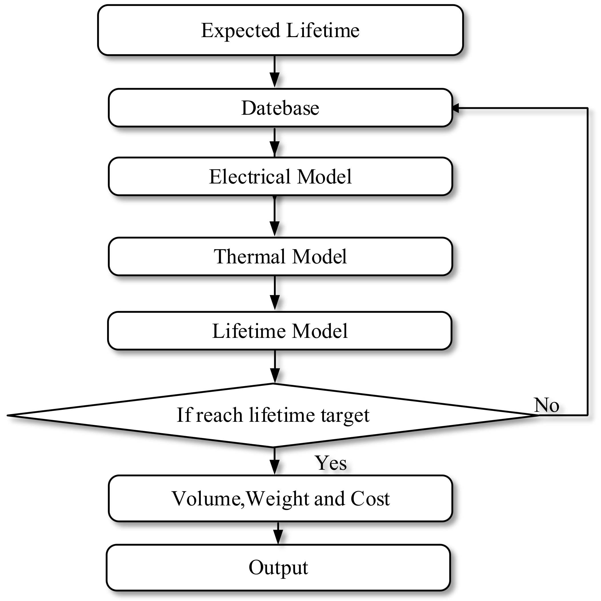
There are two reasons to study the reliability-oriented design of variable active inductors. First is the reliability requirement of the product. Magnetic inductors being reliable in power converters in common knowledge. In order to replace the magnetic inductor by using a variable active inductor, it is necessary to achieve the same level of reliability. The second reason is to identify the benefit of this technology from the practical of view. The comparison of the results of size, weight, and cost from magnetic inductors and active variable inductors should rely on the same reliability specifications. Then, the results would be meaningful. Based on the background, the flow chart based on reliability design is considered and shown in
Figure 3.
The reliability-oriented design flowchart includes eight steps [
21,
22]. The inputs of the design are the expected lifetime and operating conditions. Suitable devices are initially selected in the component database based on the operating conditions and expected lifetime. The database contains capacitors, inductors and switching devices. Then, the power losses of capacitors and switching devices are calculated by the electrical model. The power loss is used as an input to the thermal model, and the temperature of the capacitor and switching devices during operation is obtained by thermal stress analysis. Finally, the results of the thermal stress analysis are input to the lifetime model, and the lifetime of the capacitors and power semiconductors are estimated through the lifetime model. If the lifetime fulfills the expected requirements, the physical characteristics of the active inductor can be exported, otherwise, the devices continue to be reselected in the database until the expected lifetime is fulfilled [
3].
3.1. Capacitor
3.1.1. Capacitor Selection
The voltage stress and current stress of the capacitor should be determined based on the operating conditions of the system before selecting the capacitor. For the active inductor module, the capacitor voltage to complete the DC-link capacitive energy conversion should satisfy as:
The current stress of the capacitor, by ignoring the power loss of the converter, can be calculated by the law of conservation of energy as:
where
is the current flowing through the active inductor which can be calculated by the method in [
23]. The final step in capacitor selection is to obtain the capacitance of the DC link from [
23].
3.1.2. Electrical Model
The hotspot temperature of the capacitor changes with the power loss of the capacitor and affects the lifetime of the capacitor. Therefore, the power loss of capacitor is an important factor in determining its lifetime. The power loss of the capacitor can be calculated as [
3]:
where
is the Equivalent Series Resistance (ESR) of the capacitor when the current frequency is
, and
is the Root Mean Square (RMS) value of the harmonic current at the frequency
. The ESR of the capacitor and the RMS of the current can be derived from the electrical model.
3.1.3. Thermal Model
For electrolytic capacitors, the high temperature of the capacitor will accelerate the electrolyte vaporization and lead to the aging of the capacitor [
3]. Based on the power loss of the capacitor derived in the previous step, the hotspot temperature of the capacitor can be calculated from the thermal model of the capacitor [
3]:
where
is the ambient temperature,
is the thermal resistance of the capacitor hotspot to the environment.
3.1.4. Lifetime Model
For electrolytic capacitors, a generic lifetime model is as follows [
3]:
where
and
are the lifetime under operating and test conditions, respectively.
and
are the voltages under operating and test conditions, respectively.
and
are hotspot temperatures under operating and test conditions, respectively. The value of n for electrolytic capacitors usually varies from 3 to 5.
3.2. Power Semiconductors
3.2.1. Power Semiconductor Selection
The selection of the power semiconductor depends on its electrical stress and the required switching frequency of the system. The structure and principle of the active inductor circuit show that the voltage stress
and current stress
of the switching device are:
3.2.2. Power-Loss Calculation
Power loss of power semiconductors mainly includes conduction loss and switching loss [
24]:
The conduction loss includes the conduction loss of the switching device
and
the equivalent diode [
24]:
where
is equal to Iindrms,
is the on-resistance of the switching device,
and
are the zero-current voltage of the diode on state and the diode on-state resistance, respectively.
and
are the transient currents flowing through the switch and diode, respectively.
is the average diode current and
is the root mean square diode current. The above parameters can be obtained from the data sheet of the switching device.
Power semiconductor switching loss consists of switching device loss and diode loss. The diode conduction loss can be ignored, and the switching loss is the product of switching energy and switching frequency:
where
and
are the turn-on energy loss and turn-off energy loss of the switching device, respectively,
is the switching frequency and
is the turn-on energy of the diode.
3.2.3. Thermal Model
The temperature variation of a power semiconductor is determined by the power loss and thermal resistance of the power semiconductor [
24]:
where
is the thermal resistance from the junction to the case,
is the thermal resistance from the case to the heat sink, and
is the thermal resistance of the heat sink to ambient.
3.2.4. Lifetime Model
The Bayerer model, which is a more comprehensive analytical model, is used for the prediction of power-switch lifetime. When using this model, it is important to specify the experimental conditions involved in the model before making lifetime predictions for the device [
25]. The model equation is as follows:
where A,
to
are constants that can be proposed after data fitting,
is the junction temperature variation of the power switch and
is the maximum junction temperature of the power switch,
is the on-time of the power switch during the power cycle.
3.3. Inductor
The inductor has less degradation compared to power switches and capacitors, so the lifetime of the inductor is not considered in this paper. The selection of inductors is based on the Total Harmonic Distortion (THD) and ripple-current requirements of the inductor current. In addition, electrical stresses should be satisfied.
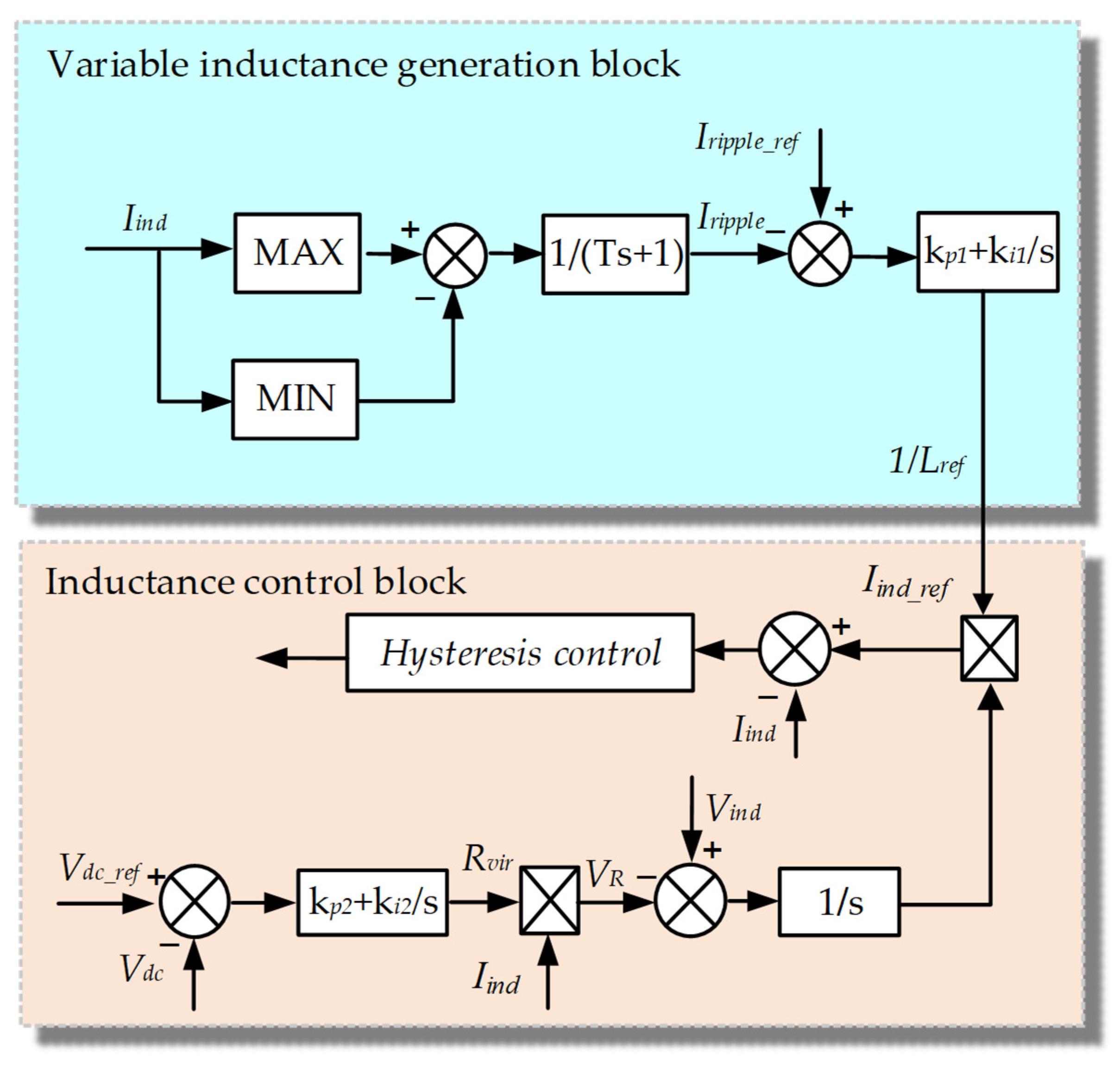
4. Variable Inductance Control for Performance Improvement
The control of the variable inductor includes two parts. The first part aims to generate the equivalent inductance reference based on the terminal information of the variable inductor. Another part is to realize this equivalent inductance reference by using closed-loop current control. The control diagram is shown in
Figure 4. The parameter definitions are shown below.
Vdc_ref is the reference voltage of Cdc,
Vdc is the actual voltage of the Cdc,
Rvir is the virtual impedance of the active inductor,
Iind is the current flowing through the active inductor,
Iind_ref is the current reference value of the active inductor,
VR is the virtual impedance voltage,
Vind is the active inductor port voltage,
Lref is the reference value of the equivalent inductance of the active inductance,
Iripple_ref is the reference value of active inductor ripple current,
Iripple is the actual ripple current of the active inductor.
In the equivalent inductance reference generation block, the input is the DC-link current limit and the measured DC-link current. By extracting the peak-to-peak current ripple and comparing it with the ripple limit, the control error can be obtained. Through a PI controller, the inductance reference can be derived. If the measured ripple is higher than the limit, the equivalent inductance value will increase to reduce the ripple, otherwise it will reduce to enlarge the ripple component.
In the inductance control block, there are two loops to achieve the certain inductance value and stabilize the variable inductor. The outer loop is the low-speed loop, used to stabilize the DC-link voltage inside of the active inductor. During operation, the active inductor will consume energy to support the power loss of the switches, filters, and other auxiliary components. The DC-link voltage inside of the active inductor could drop continually if there is no additional energy compensation. By using the voltage outer loop, the active power will be absorbed by the variable inductor to maintain the constant DC-link voltage. The input of the outer loop is the DC-link reference voltage and the measured voltage. Through a PI controller, the equated loss of a series’ virtual resistance R
vir can be obtained. The product of the virtual resistance and the inductor current is the voltage drop of the virtual resistance, V
R. This result is subtracted from the port voltage, V
ind, to be the actual voltage drop of the inductor. The voltage of the inductor obtained through the voltage loop is used as the input to the current loop. The function of the current loop is to track the reference current calculated from the equivalent inductance reference. The current loop controls the current of the active inductor according to following equation.
The resulting current error signal is fed to the hysteresis controller to generate the drive signals for the power switches that control the operation of the H-bridge, and the terminal impedance is controlled as a magnetic inductor by the current loop.
Simulation results of an ASD system with a magnetic inductor and variable active inductor are provided for comparison to support the theoretical analysis in
Figure 5. In the ASD system with the passive magnetic inductor, when the grid voltage is balanced, the grid-side current is a continuous current. There are 6-times the fundamental current at the DC link and the load side, as shown in the red curve. In the system when the active inductor replaces the passive inductor, it can be seen that the waveforms are totally overlapped, which means the active variable inductor can achieve the same performance as the passive magnetic inductor in this ASD system. It proves the functionality of the fixed-inductance control method.
The simulation results prove the variable inductance control as shown in
Figure 6. The test condition is 3% unbalanced grid-voltage amplitude. When the grid voltage becomes unbalanced, the three-phase diode bridge rectifier will be forced into the single-phase operation mode. There it will introduce two times the fundamental frequency oscillation at the DC link beside six times the fundamental oscillation. The cut-off frequency of the low-pass filter is 10 Hz. Kp1 and Ki1 are 1 and 150, respectively. Kp2 and Ki2 are 0.03 and 0.5, respectively. The bandwidth of the hysteresis controller is 0.5 A. By using the existing magnetic inductor, the filter characteristic is constantly fixed, therefore, the oscillations at the grid unbalances are severe. However, when the ASD system is implemented with the variable active inductor, the equivalent inductance is adaptively increased from 2.5 mH to 8 mH with the DC-link oscillation, instead of fixed filtering characteristics. From the simulation, it can be seen that the DC-link ripple and the load-current ripple can be reduced significantly, due to the equivalent inductance of the variable active inductor being updated automatically from 2.5 mH to 8 mH. As a comparison, the DC-link ripple of the magnetic inductor is much higher than the expected, which raises the stress of the inverter stage and could lead to higher failure rate and shorter lifetime.
5. Experimental Verification of the Variable Inductor
A prototype is built in the lab to prove the physical characteristics of the variable active inductor, which is shown in
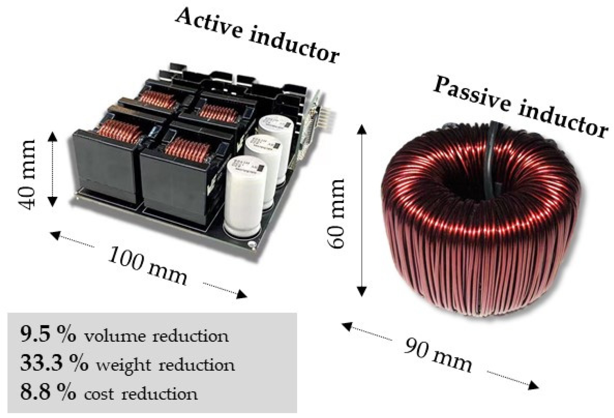
Figure 7. It is designed for the DC link of a 7.5 kW ASD system. In order to emulate the operating condition of the ASD system, an equivalent testing system is built in the lab. The first stage uses a programmable voltage source to emulate the grid voltage, and then is connected with a front-end diode bridge rectifier. The load inverter is simplified by using a resistor load. Unbalanced grid voltage at 3% amplitude at one phase is considered to emulate the unbalanced grid-voltage case. Even though the harmonics content is different from the real case, the low-frequency six times and two times the fundamental frequency harmonics are the same with the field applications. Therefore, it has no effect on the accuracy of the experimental verification. The prototype built in the lab is shown below. There are two PCBs assembled together, where one board is the power stage and another one is the conditioning and controller circuit. Separate design could reduce the noise transmission from the power stage to the signal stage. From the pictures of the prototypes, it can be seen that the variable active inductor has a smaller size, lighter weight, and lower height compared with the passive magnetic inductor. The estimated power loss of the device, capacitor, and filter inductor are 2.5 W, 1.8 W and 10 W, respectively. The control frequency of the prototype is 20 kHz to track the harmonics at six times and two times fundamental frequency. The control parameters are shown below. The detailed comparison and the verification of the control methods are discussed below.
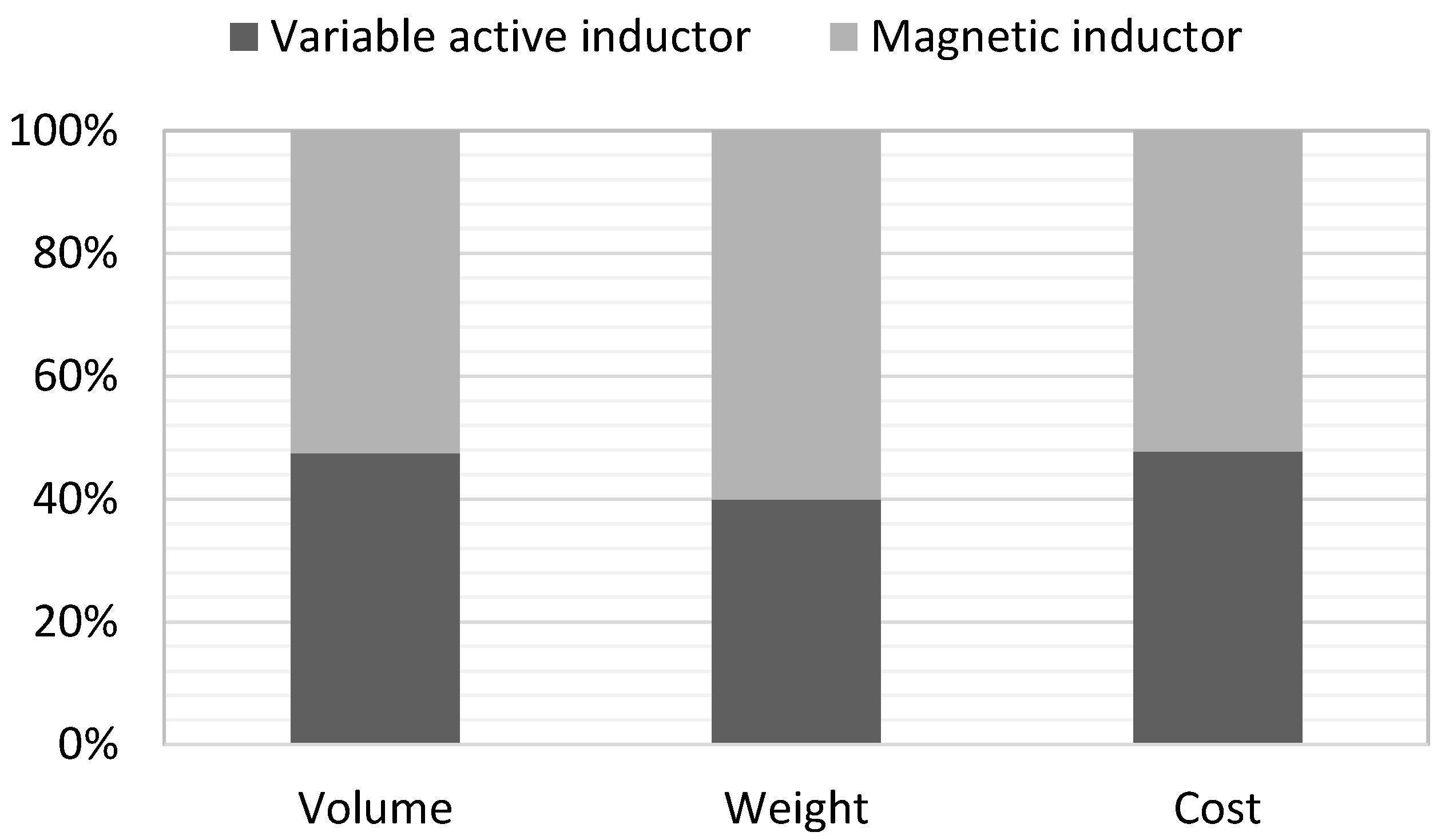
5.1. Physical Characteristics Comparison between Magnetic and Active Inductor
The physical characteristics are compared between magnetic and active inductor, with results shown in
Table 2. The active inductor component selection is based on the reliability-oriented component sizing procedure, where the designed lifetime is 10 years. For the passive magnetic inductor, it is commonly assumed that it is much reliable compared with the components in the power converter, so the reliability is sufficient. In this case, the physical characteristics can be benchmarked, and the results are shown in
Figure 8. It can be seen that all the physical characteristics can be optimized by using a variable active inductor, especially the weight of the active inductor. By using the semiconductor circuit, the weight is much lower than the magnetic-core- and copper-coil-based inductor, which is a great contribution to weight-sensitive applications, such as EV, traction, aircraft and so on.
5.2. Verification of the Electrical Characteristics of the Variable Inductor under Balanced Grid Condition
The first step to prove the effectiveness of the active variable inductor is to compare the electrical performance with the magnetic inductor with the same inductance value. Due to the power limit in the lab, downscale testing is conducted, where the experimental results of the ASD with the active inductor is shown in
Figure 9. It can be seen that when the grid voltage is balanced, there will be six times the fundamental frequency at the DC link. From the comparison in (a–d), it can be seen that the variable active inductor can achieve the same performance as the passive magnetic inductor. Therefore, it can work well and replace it for the normal operation.
5.3. Verification of Electrical Characteristics of the Variable Inductor under Unbalanced Grid Condition
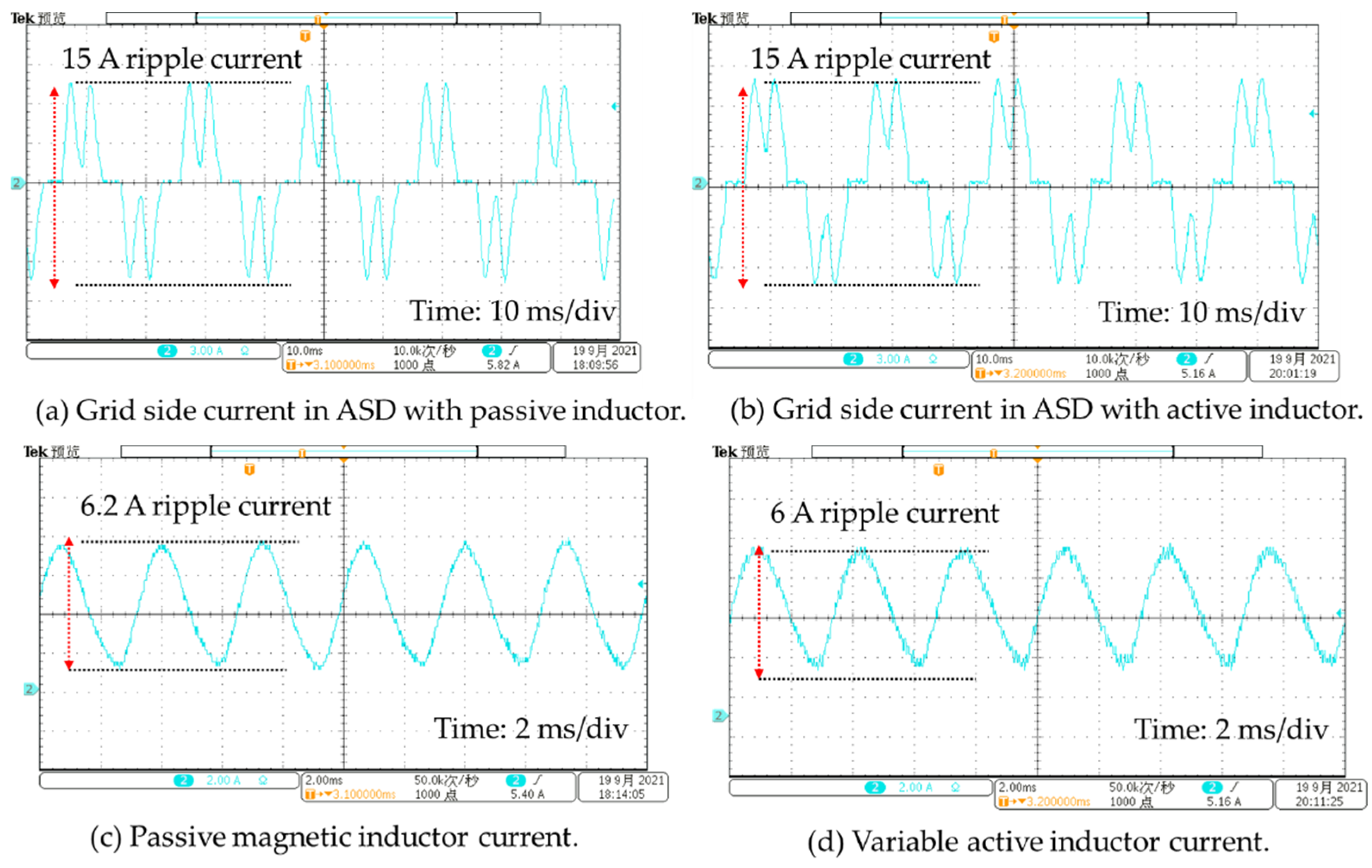
In real applications, the unbalanced grid voltage will introduce two times the fundamental harmonics at the DC link. The existing fixed inductor cannot filter out these harmonics, leading to high oscillation. The proposed variable active inductor can adaptively change the inductance value to mitigate the high ripple. Experimental testing to prove the effectiveness of the variable active inductor in the unbalanced grid voltage conditions are shown in
Figure 10. It can be seen that when the grid voltage is unbalanced, the grid-side current will distort and the DC-link current will have a higher ripple, which includes both six times the fundamental harmonics and the two times the fundamental harmonics. By using the active variable inductor, the harmonics at the DC link can be reduced to 60% of the ripple in the passive inductor case study. This will be helpful to reduce the stress and enhance the stability of the motor-drive system.
6. Discussion and Future Perspectives
This paper studies the benefits of the active inductor compared with the conventional magnetic inductor from the practical point of view and proposes a novel variable active inductor for the performance improvement of motor drive, considering real grid conditions. Even though it has been fully discussed and the concept has been proven, there are still some interesting aspects to be studied in the future:
The benefits of the active inductor at a range of power rating applications are different. It is necessary to model the performance in a wide range and identify the best region for use.
The applications of variable inductor are not limited to the DC link. It can also be used as the fixed AC magnetic inductor and variable AC inductor. The corresponding circuit structure and control are necessary to be studied in the future.
The plug-and-play functionality is preferred due to the conventional magnetic inductor being a two-terminal component, which is easy to use. Practical design and implementation are interesting to study.
There are also application limits to the variable inductor. For high-frequency harmonics applications, such as kHz and MHz, ultrahigh-frequency switching devices are needed to implement the variable active inductor. The benefit of the variable inductor is not clear. The physical characteristics and cost could limit the application of the variable inductor, which requires further study.
7. Conclusions
This paper proposes a novel variable inductor for the DC link of an ASD system. It can adaptively change the inductance under different conditions and effectively improve the electrical and physical characteristics in principle. The reliability-oriented design is first studied to demonstrate the benefits of the variable active inductor. All the components are based on the same design procedures and same reliability targets, so that the comparison between solutions is more useful. It considers the practical factors (e.g., size, weight, cost, and reliability) compared to the proof-of-concept studied in previous work. A novel variable inductance control method is proposed to stabilize the system under normal and abnormal operating conditions. The key conclusions are summarized below:
Based on the reliability-oriented design, the physical characteristics in terms of size, weight, and cost of the variable inductor for the commercial products can be reduced to maximum of 30%;
By online adaptive tuning the inductance value, the oscillation at the DC link can be mitigated at both the unbalanced and balanced grid voltage conditions.
Author Contributions
Conceptualization, Q.W. and B.L.; methodology, Z.K. and F.L.; validation, Z.K., and F.L.; investigation, Z.K., J.W.; data curation, Z.K., J.W.; writing—original draft preparation, Q.W. and Z.K.; writing—review and editing, Q.W. and B.L.; supervision, Q.W. and B.L. All authors have read and agreed to the published version of the manuscript.
Funding
This work was supported by project of National Natural Science Foundation of China (Grant No: 51777146, 51977163).
Data Availability Statement
Data available in a publicly accessible repository.
Conflicts of Interest
The authors declare no conflict of interest.
References
- Zare, F.; Soltani, H.; Kumar, D.; Davari, P.; Delpino, H.A.M.; Blaabjerg, F. Harmonic emissions of three-phase diode rec-tifiers in distribution networks. IEEE Access 2017, 5, 2819–2833. [Google Scholar] [CrossRef]
- Hinkkanen, M.; Luomi, J. Induction motor drives equipped with diode rectifier and small dc-link capacitance. IEEE Trans. Ind. Electron. 2008, 55, 312–320. [Google Scholar] [CrossRef]
- Wang, H.; Blaabjerg, F. Reliability of Capacitors for DC-Link Applications in Power Electronic Converters—An Overview. IEEE Trans. Ind. Appl. 2014, 50, 3569–3578. [Google Scholar] [CrossRef] [Green Version]
- Wen, H.; Xiao, W.; Wen, X.; Armstrong, P. Analysis and Evaluation of DC-Link Capacitors for High-Power-Density Electric Vehicle Drive Systems. IEEE Trans. Veh. Technol. 2012, 61, 2950–2964. [Google Scholar] [CrossRef]
- Rajashekara, K.S.; Rajagopalan, V.; Sevigny, A.; Vithayathil, J. DC Link Filter Design Considerations in Three-Phase Voltage Source Inverter-Fed Induction Motor Drive System. IEEE Trans. Ind. Appl. 1987, IA-23, 673–680. [Google Scholar] [CrossRef]
- Dzhankhotov, V.; Pyrh¨onen, J. Passive LC Filter Design Considerations for Motor Applications. IEEE Trans. Ind. Electron. 2013, 60, 4253–4259. [Google Scholar] [CrossRef]
- Council of European Energy Regulators (CEER). 5th Ceer Benchmarking Report on the Quality of Electricity Supply; Council of European Energy Regulators (CEER): Brussels, Belgium, 2011. [Google Scholar]
- Kolar, J.W.; Friedli, T. The Essence of Three-Phase PFC Rectifier Systems—Part I. IEEE Trans. Power Electron. 2013, 28, 176–198. [Google Scholar] [CrossRef]
- Wang, H.; Davari, P.; Wang, H.; Kumar, D. Lifetime estimation of DC-Link capacitors in adjustable speed drives under grid voltage unbalances. IEEE Trans. Power Electron. 2019, 34, 4064–4078. [Google Scholar] [CrossRef]
- Von Jouanne, A.; Banerjee, B. Assessment of voltage unbalance. IEEE Trans. Power Deliv. 2001, 16, 782–790. [Google Scholar] [CrossRef]
- Wang, H.; Liserre, M.; Blaabjerg, F. Toward reliable power electronics: Challenges, design tools, and opportunities. IEEE Ind. Electron. Magazine 2013, 7, 17–26. [Google Scholar] [CrossRef] [Green Version]
- ANSI C84.1. American National Standard for Electric Power Systems and Equipment-Voltage Ratings (60 Hertz); NEMA: Rosslyn, VA, USA, 2006. [Google Scholar]
- Lee, K.; Jahns, T.; Venkataramanan, G.; Berkopec, W. DC bus electrolytic capacitor stress in adjustable-speed drives under input voltage unbalance and sag conditions. In Proceedings of the Conference Record of the 2004 IEEE Industry Applications Conference, 2004. 39th IAS Annual Meeting, Seattle, WA, USA, 3–7 October 2004. [Google Scholar] [CrossRef]
- Wang, H.; Wang, H. Capacitive dc links in power electronic systems reliability and circuit design. Chin. J. Elect. Eng. 2018, 4, 29–36. [Google Scholar]
- Wang, H.; Wang, H.; Zhu, G.; Blaabjerg, F. An overviewof capacitive dc links—Topology derivation and scalability analysis. IEEE Trans. Power Electron. 2020, 35, 1805–1829. [Google Scholar] [CrossRef]
- Wang, H.; Wang, H. A two-terminal active capacitor. IEEE Trans. Power Electron. 2017, 32, 5893–5896. [Google Scholar] [CrossRef]
- Funato, H.; Kawamura, A. Proposal of variable active-passive reactance. In Proceedings of the 1992 International Conference on Industrial Electronics, Control, Instrumentation, and Automation, San Diego, CA, USA, 13–13 November 1992; Institute of Electrical and Electronics Engineers (IEEE): Piscataway, NJ, USA, 2003; pp. 381–388. [Google Scholar]
- Rana, D.; Hafez, B.; Garg, P.; Essakiappan, S.; Enjeti, P. Analysis and design of active inductor as DC-link reactor for lightweight adjustable speed drive systems. In Proceedings of the 2014 IEEE Energy Conversion Congress and Exposition (ECCE), Pittsburgh, PA, USA, 14–18 September 2014; Institute of Electrical and Electronics Engineers (IEEE): Piscataway, NJ, USA, 2014; pp. 3243–3250. [Google Scholar]
- Dai, W.; Enjeti, P.; Qiu, D. Advanced active output filter for low acoustic noise adjustable speed drive (ASD) system. In Proceedings of the 2016 IEEE International Power Electronics and Motion Control Conference (IPEMC-ECCE Asia), Hefei, China, 22–26 May 2016; pp. 3646–3653. [Google Scholar]
- Das, J. Passive filters-potentialities and limitations. IEEE Trans. Ind. Appl. 2003, 40, 232–241. [Google Scholar] [CrossRef]
- Wang, H.; Wang, H. Performance evaluation of a two-terminal active Inductor in the DC-link filter of a three-phase di-ode bridge rectifier. In Proceedings of the IEEE APEC, Anaheim, CA, USA, 17–21 March 2019; pp. 2844–2848. [Google Scholar]
- Wang, H.; Wang, H. A Two-Terminal Active Inductor with Minimum Apparent Power for the Auxiliary Circuit. IEEE Trans. Power Electron. 2019, 34, 1013–1016. [Google Scholar] [CrossRef]
- Sakui, M.; Fujita, H.; Shioya, M. A method for calculating harmonic currents of a three-phase bridge uncontrolled rectifi-er with DC filter. IEEE Trans. Ind. Electron. 1989, 36, 434–440. [Google Scholar] [CrossRef]
- Graovac, D.; Pürschel, M.; Kiep, A. MOSFET Power Losses Calculation Using the DataSheet Parameters. Infineon Technologies AG. Available online: www.infineon.com (accessed on 31 July 2006.).
- Bayerer, R.; Herrmann, T.; Licht, T.; Lutz, J.; Feller, M. Model for Power Cycling lifetime of IGBT Modules - various factors influencing lifetime. In Proceedings of the 2008 International Conference on Integrated Power Electronics Systems, Nuremberg, Germany, 11–13 March 2008; pp. 1–6. [Google Scholar]
| Publisher’s Note: MDPI stays neutral with regard to jurisdictional claims in published maps and institutional affiliations. |
© 2021 by the authors. Licensee MDPI, Basel, Switzerland. This article is an open access article distributed under the terms and conditions of the Creative Commons Attribution (CC BY) license (https://creativecommons.org/licenses/by/4.0/).


