Article

Multi-Level Control of Resistive RAM (RRAM) Using a Write Termination to Achieve 4 Bits/Cell in High Resistance State

1
M2NP, UMR CNRS 7334, Aix-Marseille Université, 38 rue Joliot Curie, F-13451 Marseille, France
2
Computer Engineering Laboratory, Delft University of Technology, Mekelweg 4, 2628 CD Delft, The Netherlands
3
LIRMM, University of Montpellier/CNRS, F-34095 Montpellier, France
*
Author to whom correspondence should be addressed.
Electronics 2021, 10(18), 2222; https://doi.org/10.3390/electronics10182222
Submission received: 10 August 2021 / Revised: 26 August 2021 / Accepted: 7 September 2021 / Published: 10 September 2021
(This article belongs to the Section Microelectronics)

Abstract

:
RRAM density enhancement is essential not only to gain market share in the highly competitive emerging memory sector but also to enable future high-capacity and power-efficient brain-inspired systems, beyond the capabilities of today’s hardware. In this paper, a novel design scheme is proposed to realize reliable and uniform multi-level cell (MLC) RRAM operation without the need of any read verification. RRAM quad-level cell (QLC) capability with 4 bits/cell is demonstrated for the first time. QLC is implemented based on a strict control of the cell programming current of 1T-1R HfO2-based RRAM cells. From a design standpoint, a self-adaptive write termination circuit is proposed to control the RESET operation and provide an accurate tuning of the analog resistance value of each cell of a memory array. The different resistance levels are obtained by varying the compliance current in the RESET direction. Impact of variability on resistance margins is simulated and analyzed quantitatively at the circuit level to guarantee the robustness of the proposed MLC scheme. The minimal resistance margin reported between two consecutive states is 2.1 kΩ along with an average energy consumption and latency of 25 pJ/cell and 1.65 μs, respectively.

1. Introduction

Memory is an essential component of today’s electronic systems. It is used in any equipment using a processor such as computers, smart phones, digital cameras, automotive systems, etc., [1]. Moreover, the unprecedented growth in Internet of Things (IoT) devices across all industry verticals continuously generates a massive amount of data which increases the demand for even more physical space for memory. This trend is further accelerated due to the booming increase in artificial intelligence (AI) applications and particularly edge-AI applications which require processing and storage of data at the same physical location [2]. Different alternative memory concepts have been explored in the last twenty years aiming to overcome the major limitations of existing semiconductor memories, i.e., the volatility of RAM’s and the slow programming of flash [3]. Among these emerging technologies, resistive RAMs (referred to as RRAM) are believed to be a good choice due to the advantages of simple structure offering low manufacturing costs, fast switching speed (~10 ns), small feature sizes (<10 nm), compatibility with current CMOS technology, and low voltage operation [4]. In an attempt to gain market share in these highly competitive emerging memory sectors, non-volatile memories (NVMs) vendors are trying to squeeze more and more capacity into constantly shrinking silicon dies, thereby optimizing both storage density and cost benefits. In general, there are three ways to increase the storage density of RRAMs [5]: crossbar structures, 3D integration, and MLC storage. Crossbar architectures are very challenging to implement. These architectures leverage the non-linear relationship between voltage and resistance of some RRAM technologies, which is essential to avoid the integration of a selector at the cell level in order to reach an optimal cell size of 4F2 [6]. However, in the absence of an access device, a large amount of leakage current (known as sneak-path current) flowing through unselected cells is inevitable, leading to the limitation of crossbar array sizes [6]. Regarding 3D, although eight-layer crossbar RRAM prototypes have been demonstrated, many of the manufacture-related issues including layer-dependent resistance variability are still not resolved [7]. Compared with the two abovementioned methods, MLC with its capability of storing more than a single bit of information in a single cell, is considered as one of the most promising properties of RRAM as it can increase the memory density without much change to current technologies. Alternatively, MLC can be combined with crossbar/3D technologies to reach integration densities never seen before. Although MLC relaxes the magnitude of the sneak currents and voltage drop problems related to crossbar and 3D approaches, the main challenge facing MLC storage is the implementation at the circuit level of programming techniques capable to tune accurately the analog resistance levels in order to go beyond 3 bits/cell, which is the current limit of the state-of-the-art.
The MLC storage characteristics of RRAM have been reported in many studies [5,8,9,10,11,12,13]. MLC can be implemented by varying the RRAM compliance current during the SET programming operation, or by varying the voltage during the RESET (RST) operation, or by varying the pulse widths and amplitudes during SET or RST operations. However, related prior works have the following shortcomings: MLC operation has been validated at the device level but design implications for MLC at the circuit and system levels remain to be explored. In particular, programming currents of the order of 500 µA [12] or 1 mA [13] have been reported at the device level which is incompatible with low power RRAM applications. Only a few studies of the prior art explore applications of MLC at the circuit level [14]. Most of the work focuses on read-out circuits [15,16,17]. Thereby, RRAM variability at the memory array level is not accounted during MLC programming operations. Also, so far, all the proposed solutions are limited to 3 bits/cell [18]. The proposed study advances the state-of-the-art by proposing a new design scheme that enables 4 bits/cell. To the authors’ knowledge, this is the first work addressing quad-level cell (QLC) operation. The study also introduces compelling MLC features that are missing or poorly achieved in other previously proposed works, including:
  • A MLC architecture based on compliance current control during the RST operation, allowing a tight control of post-programming resistances for optimal robustness. The compliance current being defined as the minimal current allowed during the RST operation.
  • An implementation at the circuit level with a minimal area overhead (i.e., dozens of transistors per bit-line) as no specialized read verification circuits are required.
  • A minimal energy consumption as high resistance levels (i.e., HRS RRAM states) are targeted.
The remainder of this paper is organized as follows. Section 2 presents the RRAM technology along with conventional MLC approaches. In Section 3, the MLC design scheme implementation is presented. Section 4 presents simulation results. Section 5 discusses the proposed MLC strategy. Finally, Section 6 concludes this paper.

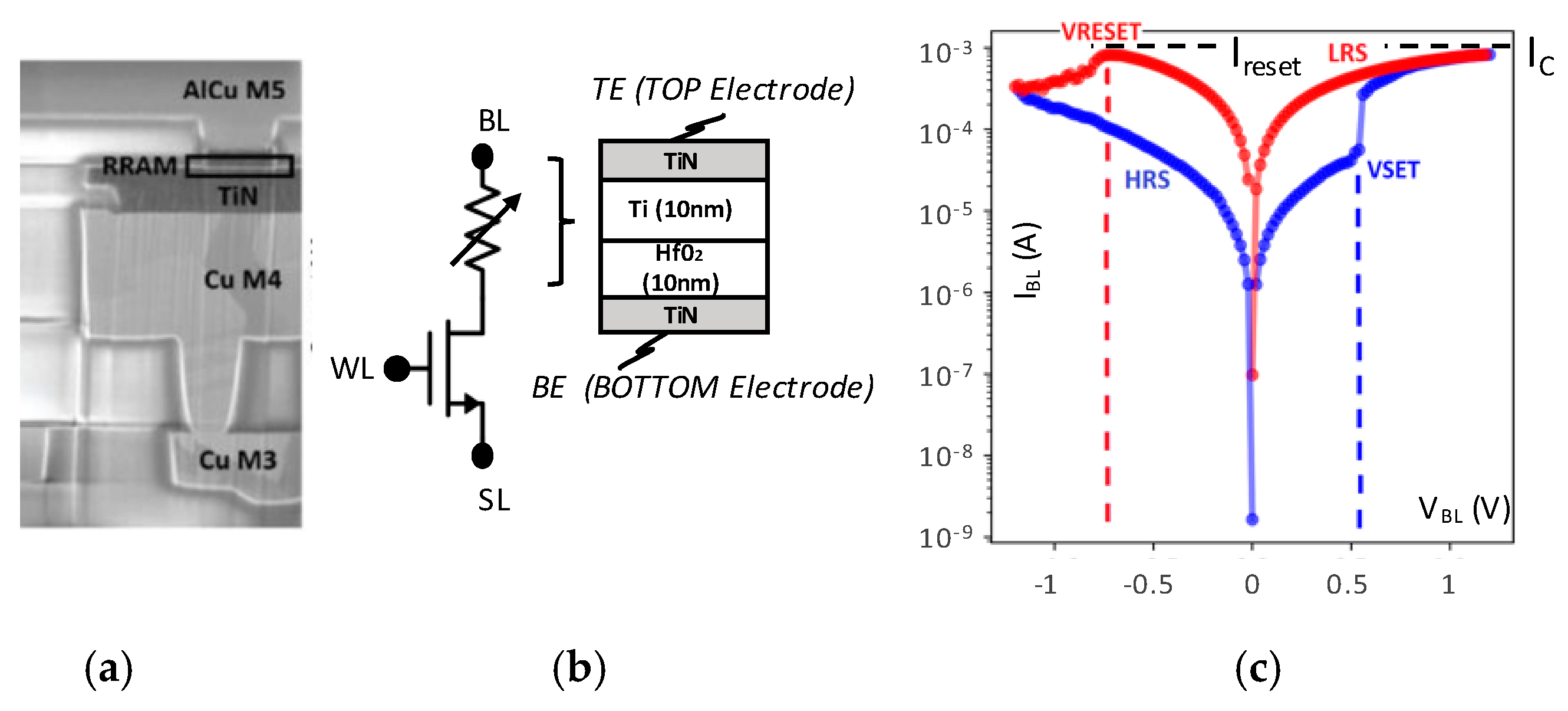
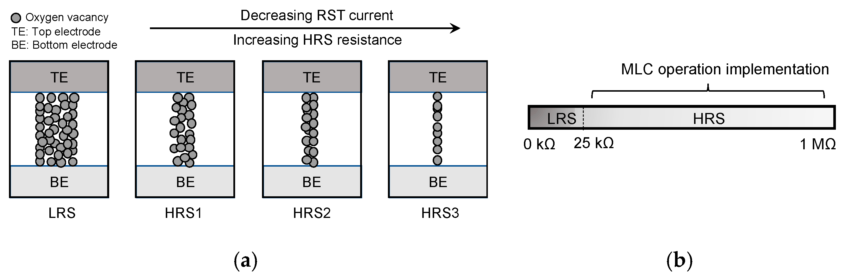
2. OxRAM Technology vs. MLC Modes

Oxide-based RRAMs memories (so-called OxRAMs) are considered in this study. An OxRAM memory cell consists of two metallic electrodes that sandwich a thin dielectric layer serving as a permanent storage medium. This metal-insulator-metal (MIM) structure, denoted RRAM in Figure 1a, can be easily integrated in the back-end of line (BEOL) on top of the CMOS subsystem. The MIM structure is integrated on top of the Metal 4 copper layer (Cu). A TiN bottom electrode (BE) is first deposited. Then, a 10 nm-HfO2/10 nm-Ti/TiN stack is added to form a capacitor-like structure [19]. Figure 1b shows the basic 1T-1R memory cell where one MOS transistor (W = 0.8 µm and L = 0.5 µm) is connected in series with an OxRAM cell. Figure 1c presents a typical 1T-1R OxRAM I-V characteristic in logarithmic scale. Based on the I-V curve, the memory cell operation can be seen as follows: after an initial electro-FORMING step [19], the memory element can be reversibly switched between the low resistance state (LRS) and the high resistance state (HRS). Resistive switching corresponds to an abrupt change between the HRS and the LRS. The resistance change is triggered by applying specific biases across the 1T-1R cell, i.e., VSET to switch to LRS and VRST to switch to HRS. In the 1T-1R configuration, the transistor controls the amount of current flowing through the cell according to its gate voltage bias. The maximum current allowed by the select transistor is called the compliance current and is referred to as IC in Figure 1c. IC controls the LRS resistance value in the SET state as well as the maximal RST current Ireset. Table 1 presents the different voltage levels used during the different operating stages. Note that the FMG step, achieved one time in the device life is a voltage-induced resistance switching from an initial virgin state with a very high resistance to a conductive state and that high voltages are typically needed during FMG.

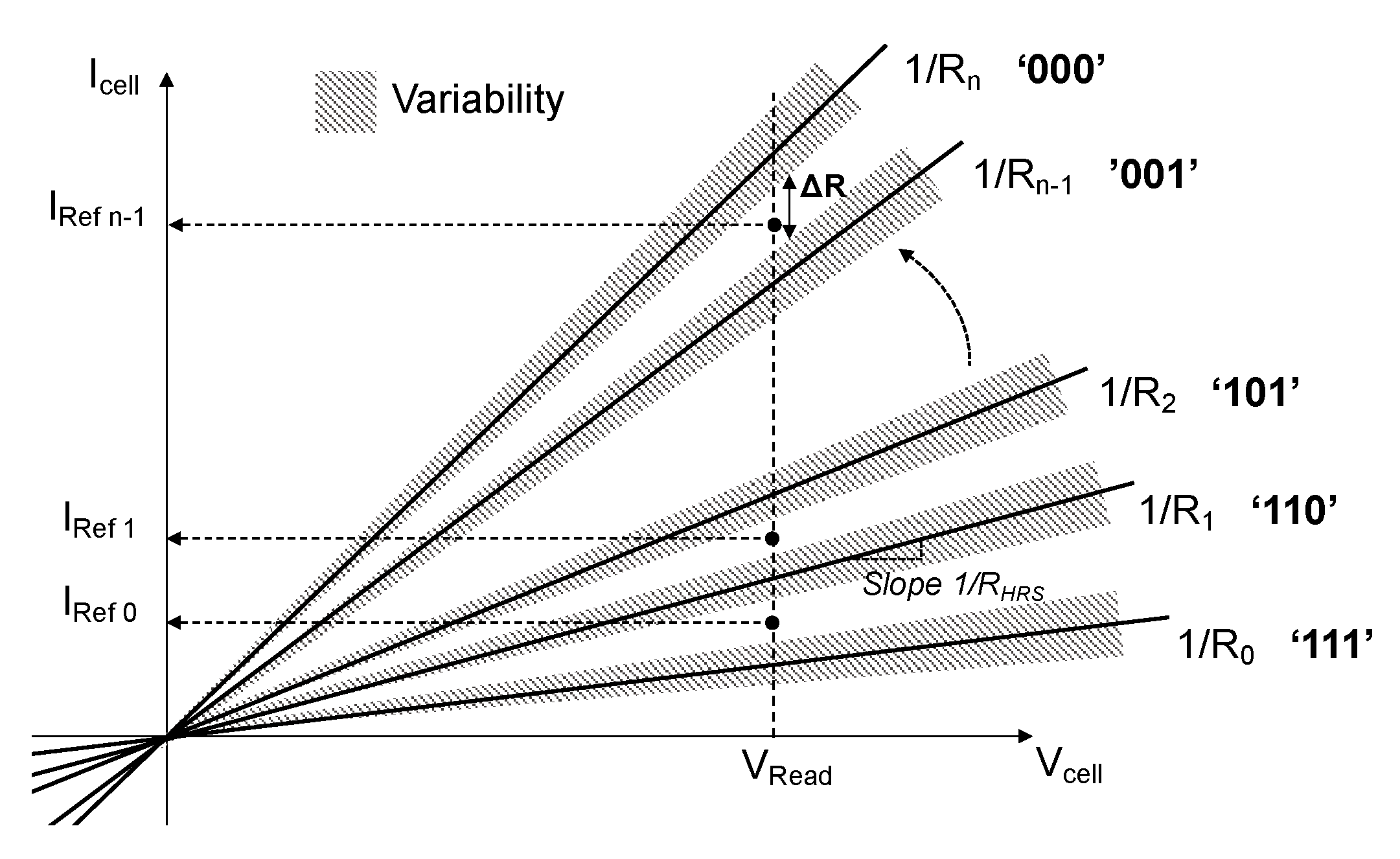
2.1. OxRAM Variability

Although OxRAM-based devices have shown encouraging properties, challenges remain, among which device variability (or reproducibility) is the main [20]. Indeed, the variance from cycle to cycle (C2C) and from device to device (D2D) can be very large, impacting directly the memory cell HRS/LRS resistance ratio. This inherent drawback of the technology has to be investigated due to its impact on MLC operation. In this regard, an 8 × 8 elementary 1T-1R array presented in Figure 2a is considered for measurements. Word lines (WLX) are used to select the active row, bit lines (BLX) are used to select active columns during a SET operation and source lines (SLX) are used to RST a whole memory word or a specific cell. Figure 2b presents the micrograph of the memory array test chip fabricated in a 130 nm CMOS technology. Experiments are performed using a B1500 semiconductor parameter analyzer (Keysight, Santa Rosa, CA, USA). The memory array is first formed. Then, memory cells are RST one by one to extract the HRS resistance. After RST, cells are SET to extract the LRS resistance. The effect of variability (combining D2D and C2C) can be seen in the cumulative probability plot shown in Figure 3 obtained after 500 consecutive RST/SET cycles applied to the memory array (500 × 64 cells). A 0.3 V READ bias voltage is used to extract RLRS and RHRS distributions. The HRS distribution spread is more pronounced compared to the LRS spread, which is a common feature of OxRAM technologies. These experimental results clearly indicate that a strict control of the HRS resistance is required to implement a reliable MLC scheme in HRS state. To mitigate the impact of variability on HRS/LRS resistances, it has been demonstrated, at the device level, that multi-step programming helps tolerate both temporal and spatial process variations to obtain uniform intermediate states [8]. However, although this method of obtaining MLC characteristics is relatively easy to implement, the approach is energy and time inefficient as it involves a sequence of programming-and-verify operations.

2.2. OxRAM Model

From a physical point of view, when a voltage VCell is applied across the OxRAM cell (i.e., between the TE and BE electrodes), depending upon the voltage polarity, one or more conductive filaments (CFs) made out of oxygen vacancies are either formed or ruptured. Once the CFs are formed inside the metal oxide to bridge the top and bottom electrodes, current can flow through the CFs, to switch the cell in a low resistance state. An interesting marker of the considered OxRAM technology is its soft-RST capability attributed to a dependency between the HRS resistance and the RST voltage or RST compliance current. The lower the RST compliance current, the thinner the CF and the higher the HRS resistance. This feature can be understood as an incomplete destruction of the CFs as shown in Figure 4a. Incomplete destruction of CFs can lead to multiple HRS levels (ranging from HRS1 to HRS3), which is believed to be the main reason for HRS variability [20]. MLC operation implementation will target the HRS state as depicted in Figure 4b to exploit the full variation range of HRS levels. Our MLC approach will consist in controlling the RST current in order to split the HRS domain into different HRS ranges equally separated. In addition to the large HRS window available for MLC, targeting the HRS, instead of the LRS domain, will result in a significant reduction in energy during the READ operations following the programming operations.
For memory array simulations, a compact OxRAM model [21,22] calibrated on measurements proposed in Section 2 is used. The model accurately reproduces the stochastic switching nature of OxRAM cells. The variation is chosen to fit experimental data as presented in Figure 5 where the model (lines) is consistent with experimental data (symbols) for SET (blue), RST (red) and FMG (green) operations. VCell is the voltage across the cell and ICell the current through the cell. A good agreement with experimental data is obtained with a ±5% standard deviation on parameters α and Lx of the model, where Lx is the OxRAM oxide thickness and α is the transfer coefficients (ranging between 0 and 1) [22].

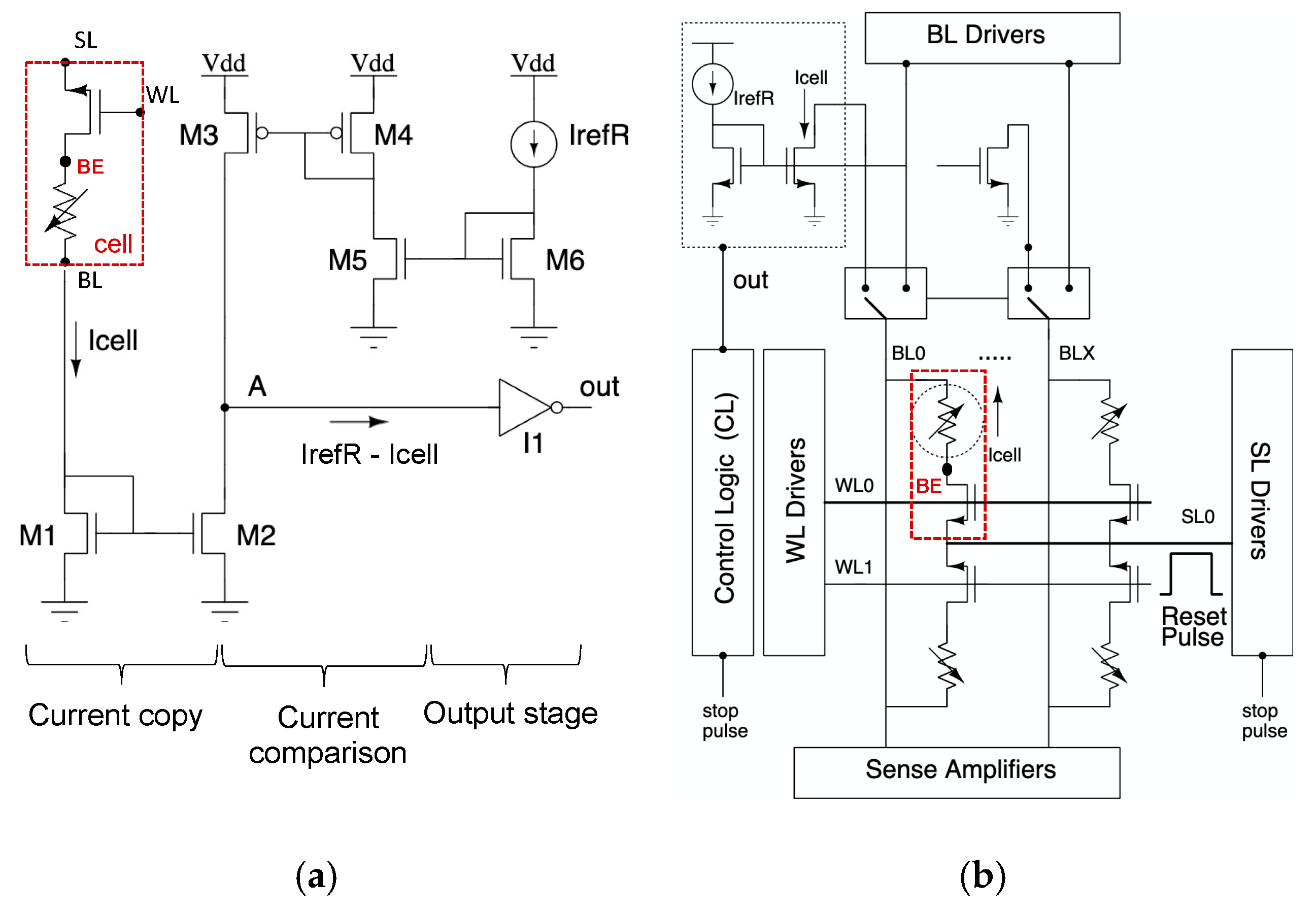
3. MLC Design Scheme

In this section, we use varying RST compliance currents to implement a robust MLC architecture. At the design level, a write termination circuit is used to constantly sense the RST current and stop the programming pulse when the preferred RST current is reached, resulting in well-defined HRS resistances.

3.1. High Level Architecture Implementation

Figure 6 shows the high-level architecture of our MLC design scheme. It consists of a regular OxRAM memory array, word line (WLX), bit line (BLX) and source line (SLX) drivers, and sense amplifiers. The drivers select active SLs, BLs and WLs during a memory operation, while the sense amplifiers convert a read current to a logical value. Eight memory cells are grouped together in a word (dashed line in the figure). The gray highlighted blocks in Figure 6 are the changes applied to the regular OxRAM memory to integrate the MLC functionality. We add one RST termination circuit per BL driver, and we modify the control logic to stop the RST operation once the cell current equals predefined reference currents. The core element of our MLC design scheme is the RST termination circuit that strictly controls the RST current in order to obtain different HRSs: during a RST operation, the circuit constantly compares the cell current to the reference current of the desired HRS. Once these currents are equal, the driver terminates the RST operation.

3.2. Low Level Architetcure Implementation

Figure 7a shows the transistor level implementation of the proposed RST termination circuit.
During the RST operation, the RRAM cell current Icell is copied by an n-MOS current mirror (M1, M2). The current mirror (M3, M4) is used to mirror the reference current IrefR (provided by M5, M6) which feeds the input of inverter I1. If (Icell − IrefR) > 0, the inverter input A is set low and the comparator output out is set to high. If (Icell − IrefR) < 0, input A is set high and out is set to low to terminate the RST operation (i.e., the RST operation is terminated when Icell decreases down to IrefR). IrefR is derived from a bandgap voltage reference circuit that is also included in a regular memory architecture to achieve stability over process, voltage and temperature [23].
Note that the RST process is a negative feedback mechanism: as the current flows from the BE to the BL, the cell resistance increases, causing current to reduce. In contrast, the SET operation is a positive feedback mechanism: as the current flows, the cell resistance is reduced, and as such, more current flows. Hence, a SET operation requires a current limitation to prevent a breakdown of the device. However, when considering MLC operation for the HRS, it is beneficial to control the RST current and terminate the RST operation when the cell current reaches a predefined minimal current, as a limit is set for the HRS resistance (i.e., the lower limit of the current is the upper limit of the HRS resistance). Figure 7b shows the usage of the termination circuit in the memory architecture. For clarity, we only show the current copy stage of the RST termination circuit. The RST operation is performed by biasing the memory cell through the SL driver while WL0 is activated. BL0 connects to the current copy stage of Figure 7a and sinks the cell current. When Icell equals IrefR (i.e., out signal is set low), the control logic triggers a stop pulse to the SL driver to terminate the RST operation.

4. Circuit Level Evaluation

4.1. MLC Concept

It is possible to define a relationship between the RST compliance current and the HRS resistance as presented in Figure 8a,b in linear and log scale respectively, to show the pseudo-exponential relation of the HRS resistance. Compliance currents are ranging from 6 μA to 36 μA and resistance values are ranging from 38 kΩ to 267 kΩ. These current and resistance ranges are considered for the MLC operation implementation. The deeper we go in the HRS state, the higher the variability [20]. Hence, the maximal HRS value is limited to 267 kΩ. This last point will be developed in the next sections. Regarding the minimal resistance, its value is set to 38 kΩ to maintain reading currents below 8 μA during READ operations.
Given the minimum and maximum HRS resistances and the number of levels required, there are different schemes in determining the resistance values, including ISO-∆R where the resistance is linearly spaced and ISO-∆I where the programming current (inverse of the resistance) is linearly spaced as described in [5]. The ISO-∆I approach is adopted as the proposed MLC scheme is based on RST current control. Table 2 presents the 16 different binary states allocated in the range (38 kΩ–267 kΩ) along with the corresponding compliance currents IrefR. It is worth noticing that each compliance current IrefR differs from the previous and the subsequent one by a constant value equal to 2 μA.
At the OxRAM device level, the resistance allocation strategy can be seen as a segmentation of the I-V plane by several I-V characteristics as shown in Figure 9. For clarity only 8 different characteristics are considered. Each characteristic is associated with a single resistance state and has a slope of 1/Rx, where x is the number of HRS states ranging from 0 to n. The precision required in the MLC operation is not only limited by the programming operation. It is also necessary to develop an accurate and robust READ mechanism. The READ operation is implemented by applying a gate voltage to the memory cells (VRead) and comparing the current drawn by the cell to currents provided by a set of reference current sources denoted by IRefx in Figure 9, where x ranges from 0 to n−1. If 8 resistance states are targeted, 7 current references are required. If 16 resistance states are targeted, 15 current references are necessary. Moreover, the DC value of each current reference needs to be located in between the current provided by two consecutive memory states which are separated by a resistance margin denoted by ΔR. Note that ΔR takes into account the variability of the n resistance states. The latter is represented by the shaded area encompassing each characteristic.

4.2. Simulation Setup

We implemented the memory circuit presented in Figure 6 using a 0.13 μm high voltage CMOS technology offering a 3.3 V supply voltage. A 3.3 V technology is required as the FMG operation involves high voltages. To verify the operation of our design scheme, SPICE simulations are performed using the Eldo simulator (Siemens, Munich, Germany). In order to accurately evaluate the benefits of our proposed scheme on large memory arrays, BL and WL lengths have been modelled to mimic a 1 Kbyte array (made of 1024 WLs and 1024 BLs). As a BL is characterized by a parasitic capacitance distributed through its length, a 1 pF bit line capacitance is used according to the targeted technology and the array architecture. Additionally, parasitic resistances [24] distributed along BLs and WLs have been inserted in the design, following the methodology developed in [25]. Based on the proposed simulation setup, after SET, RST pulses with different compliance currents are applied to the memory array. Then, HRS resistance values are extracted. More specifically, word programming is performed in two steps. Once an 8-bit word is addressed, each memory word is first entirely SET. Then a RST operation is performed in parallel through the SL with a predefined compliance current set according to the data bus values at the BL driver level. During RST, multi-bit access is guaranteed as one RST write termination is associated with a single bit-line (see Figure 7a,b).

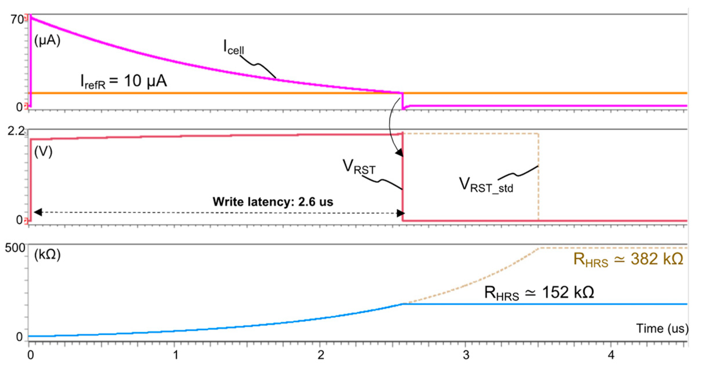
4.3. Transient Simulations

Transient simulation results are presented in Figure 10 after an RST operation associated with a compliance current equal to 10 µA. The cell current Icell gradually decreases down to IrefR set to 10 µA. Beyond this point, the RST pulse is terminated by the write termination circuit, limiting the HRS resistance value to 152 kΩ with a 2.6 µs latency. The standard RST pulse VRST_std is also reported. Adopting this standard pulse would lead to a final HRS resistance value close to 382 MΩ. Note that the standard RST pulse width is set to 3.5 µs to cover the worst cases during RST (i.e., tail bits in the switching parameter distributions [26,27]).

4.4. Monte Carlo (MC) Analysis

To assess the robustness of our MLC design scheme, a Monte Carlo (MC) analysis is conducted. In this analysis, only actual possible variations are reported, since cell variability is generated based on a targeted OxRAM technology. Moreover, the variability (including transistor mismatch [28,29]) targets the CMOS subsystem and especially the memory cell access transistor as its impact on the memory cell electrical characteristics is dominant [30]. Process variation parameters used for CMOS transistors are provided by ST-Microelectronics (Crolles, France). For each simulation run, the MC analysis calculates every parameter randomly according to statistical distribution models. The latter are provided for active devices as well as for passive devices and cover corner cases.

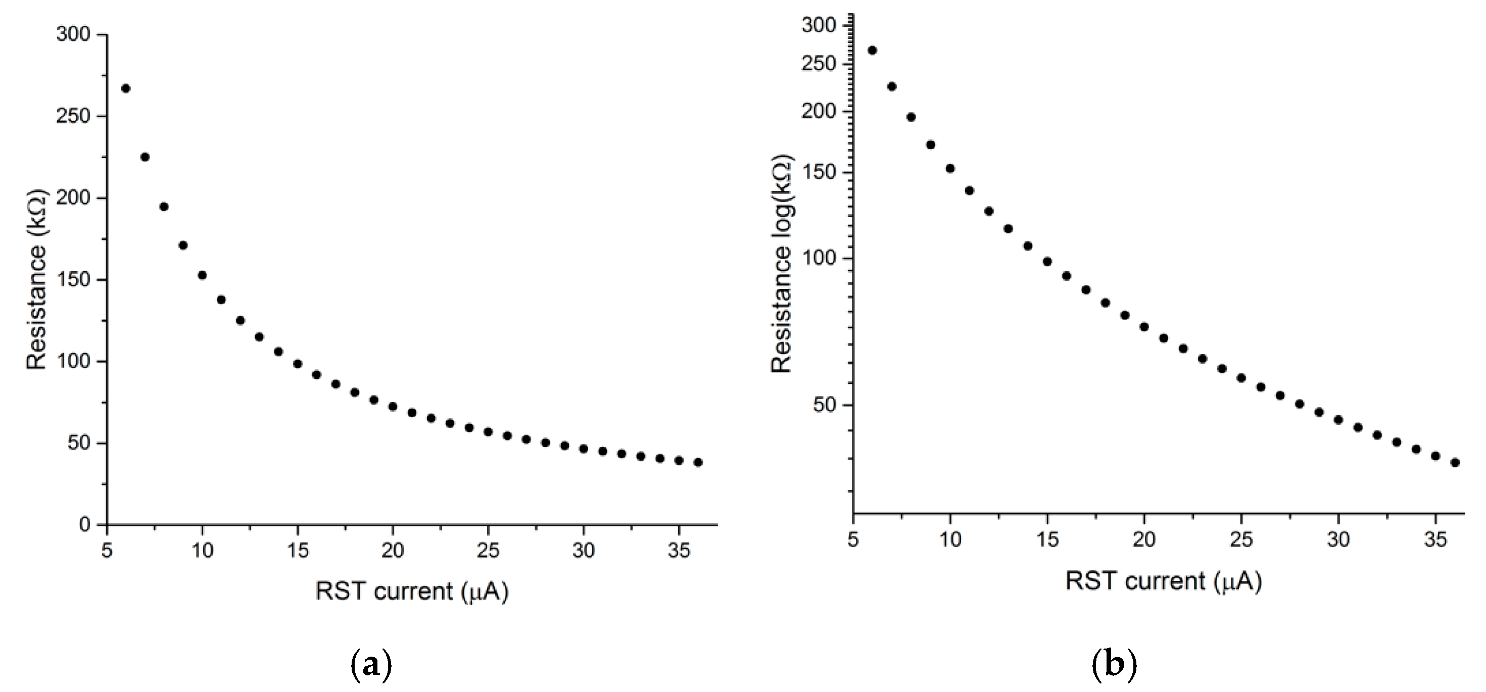
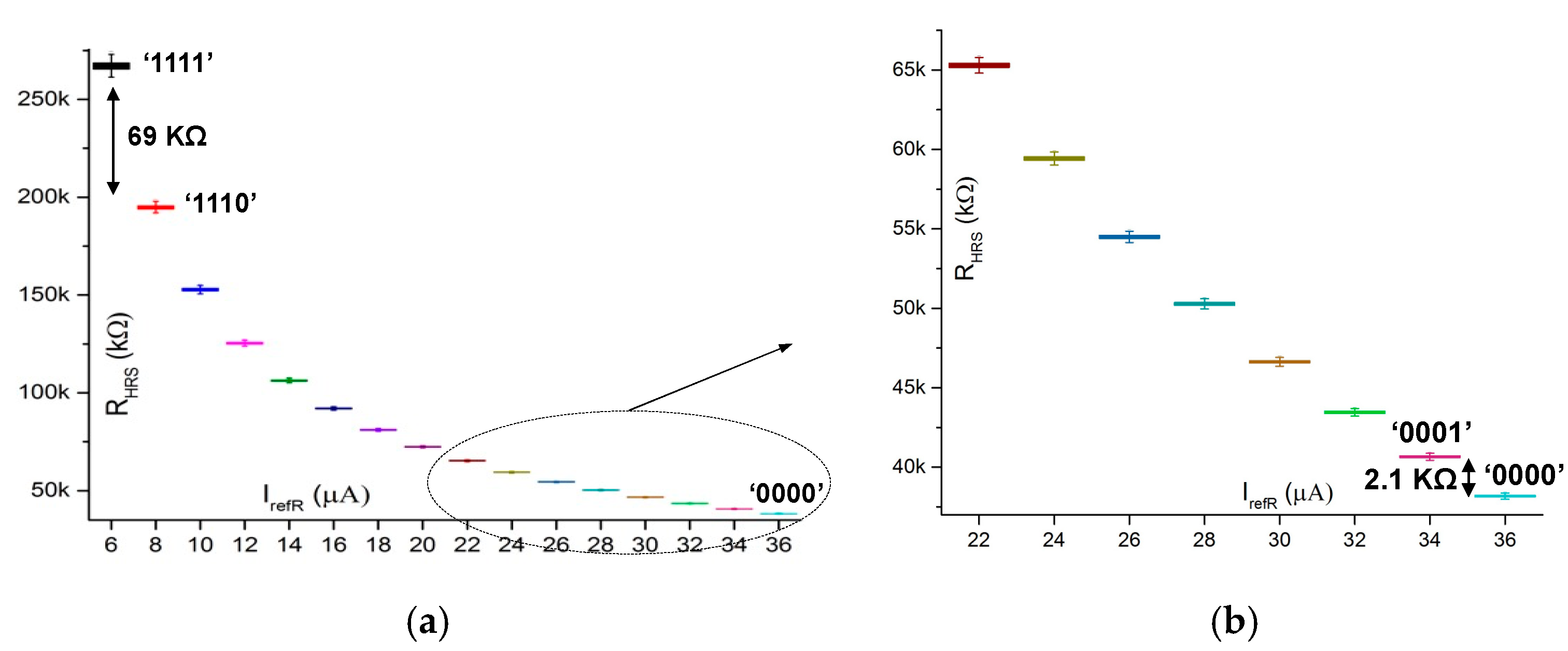
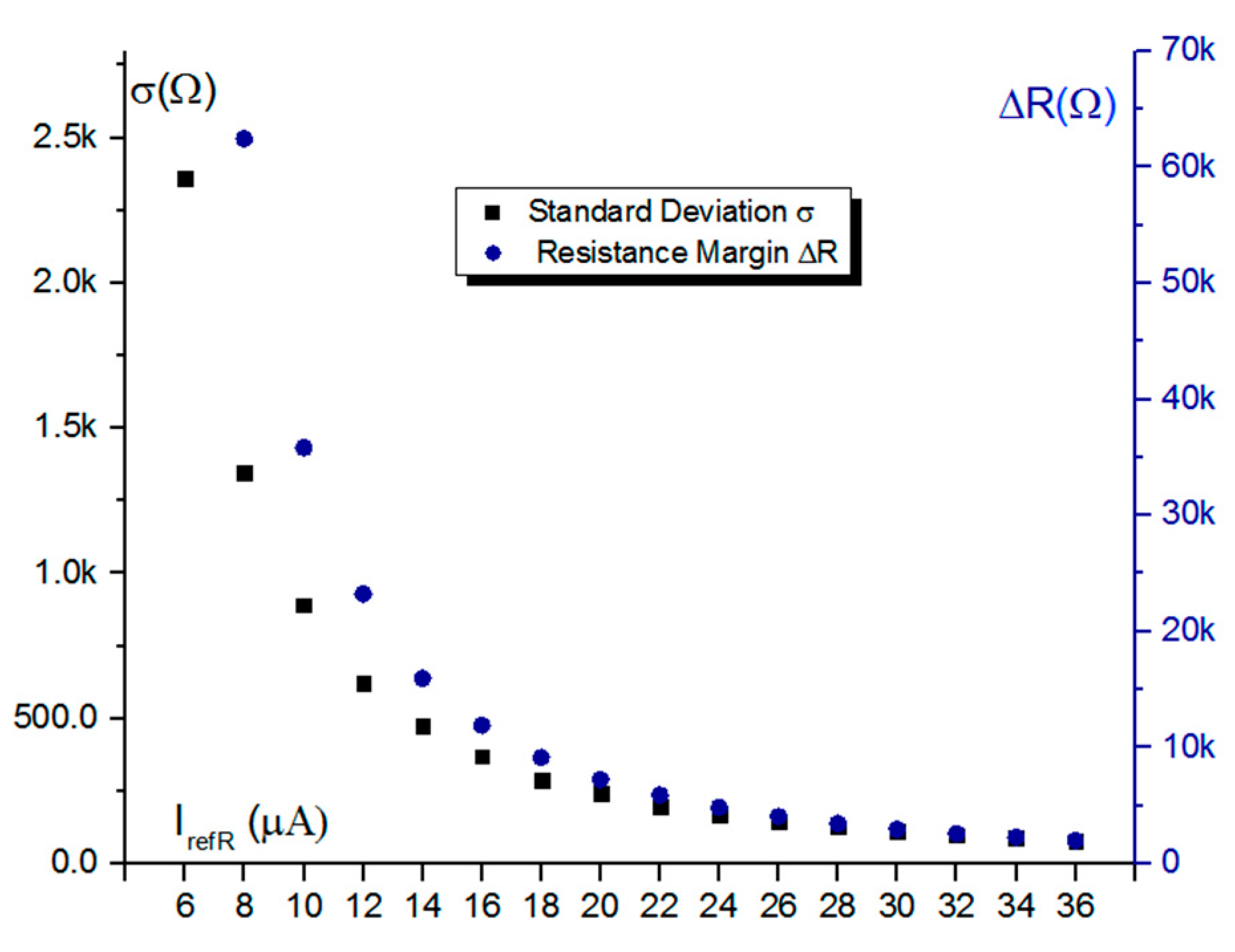
4.4.1. Quad-Level Cell (4 Bits/Cell)

Figure 11a presents the impact of variability on HRS resistance distributions in the form of box plots after 500 statistical runs following RST operations performed with the 16 compliance currents IrefR defined in Table 2 (4 bits/cell). Figure 11b shows an expanded view of Figure 11a for currents ranging from 22 µA to 36 µA. The resistance margin ranges from a minimal value of 2.1 kΩ (between states ‘0000’ and ‘0001’) to 69 kΩ (between states ‘1111 and ‘1110’). It is worth noticing that the minimal resistance margin of 2.1 kΩ is associated with the worst-case scenario where variability impacts both ‘0000’ and ‘0001’ resistance states. Moreover, this minimal margin is compliant with the resistance per unit length of copper wires used for BLs and WLs (10 Ω/µm for a 50 nm wire width [25]).
The overall uniformity of the HRS states is well-controlled. Indeed, having a strict control over the RST pulse through the RST compliance current limits the HRS resistance variation. However, when smaller IrefR values are considered, the variability of the HRS state noticeably increases, but without causing distribution overlaps, demonstrating the robustness of the proposed MLC approach.

4.4.2. Projections beyond Quad-Level Cell

Although multiple resistance levels can be easily obtained by the above-mentioned method, the successful implementation of MLC mainly depends on the ability to precisely control the resistance margin between two resistance levels. Various factors, including variability in the first place, can degrade the resistance margin and eventually lead to failures [20]. Figure 12 shows the evolution of the HRS distribution standard deviations versus the RST compliance currents associated with the 16 HRS states presented in Table 2. The resistance margin is also reported to establish a link between the standard deviation and the resistance margin evolution. We can see that standard deviation evolution follows the resistance margin one. Also, HRS standard deviation is more pronounced for low compliance currents which are associated with important HRS values. Moreover, Figure 12 reveals that the HRS standard deviation is a strong function of the compliance current and increases exponentially with decreasing compliance currents. Thus, in order to ensure sufficient margin between MLC states, we opted to increase the resistance margin with decreasing compliance currents.
Regarding the degradation of our device over time, it is possible to reach an outstanding endurance of a billion cycle for the technology considered in this paper, as shown in [19]. Furthermore, endurance and data retention issues at high temperature are mitigated by the proposed programming scheme as the final state of the cell is only determined by the current drawn by the cell and not by the resistance of the cell (i.e., the programming scheme is agnostic about resistance distribution). Thus, reliable multi-level operation is guaranteed whatever the resistance state of the memory cell and without the need of dedicated and complex write/read assist circuits [31,32,33].
Results presented in Figure 12 are in line with previous published works where it is demonstrated experimentally that variability increases as the programming current is reduced [34]. Based on these observations, our MLC approach limits the minimal compliance current to 6 µA. On the other hand, the maximal compliance current is limited to 36 µA, which results in HRS resistances of the order of 38 kΩ, limiting the maximal current bellow 8 μA for most of the time during READ operations (for a 0.3 VREAD voltage). Achieving a low read current is motivated by energy consideration, especially when dealing with low-power RRAMs [35] or read-intensive applications generally associated with in-memory processing and more specifically with neural network (NN) applications where synaptic weights are constantly and simultaneously read during inference [36,37]. Considering these compliance current boundaries (6 μA–36 µA), projection results up to 5 bits/cell and 6 bits/cell are summarized in Table 3. Moving from 4 bits/cell to 5 bits/cell results in a minimal resistance margin ∆R of 1.24 kΩ and a worst case ∆R of 490 Ω between two consecutive states. Moving up to 6 bits/cell results in a minimal ∆R of 620 Ω and a worst case ∆R of 90 Ω, making current sensing detection (i.e., capacity to recognize a state) challenging for state-of-the-art sense amplifiers [38] as the current difference sensed at 0.3 V falls below 0.5 μA. Note that worst case ∆R are related to corner case scenarios obtained after MC simulations.

5. Discussion

5.1. Performance Metrics

OxRAM operation is affected by stochastic mechanisms leading to intrinsic variability, which affects OxRAM overall performances. For this reason, OxRAM switching time (i.e., latency) and energy consumption can be degraded. The energy/cell distributions reported in Figure 13a show that low compliance currents result in higher energy dissipation due to longer RST pulses (the maximum energy reaches 150 pJ for 6 μA). The average energy/cell over the 16 states is evaluated to 25 pJ/cell. Figure 13b presents the RST latency evolution versus IrefR. The average Latency over the 16 states is evaluated to 1.65 µs. The worst-case scenario in terms of RST speed is associated with low IrefR values (the maximum latency reaches 4.01 μs for 6 μA). Latency results provided in Figure 13b do not reflect the SET operation preceding each RST operation. This is explained by the fact that the standard SET pulse is constant and common to any RST operation. The SET pulse is very short (~100 ns), which is a common feature of the considered OxRAM technology and contributes 20 pJ/cell to the total energy dissipation. Hence, in the worst case, the total energy/cell associated with a SET/RST cycle can reach 175 pJ.

5.2. Comparison with State-of-the-Art MLC Approaches

Table 4 summarizes the proposed MLC design scheme and compares it to the state-of-the-art. Comparison metrics include the targeted RRAM technology, the number of resistance states, the MLC operation mode and the design level (i.e., device or circuit level). Storing 8 states has been reported in [12,14,39,40] at the device level, mainly by varying RST voltages (VRST) and programming pulses. Our methodology is the first one to report 16 HRS resistance levels, which is a major step forward compared to the state-of-the-art. The approach leveraging on compliance current (IC) control in the RST direction, proposed in [14], is extended to 4 bits/cell. The only approach implemented at the circuit level is developed in [17]. However, this approach only considers the read operation of MLC RRAMs where the current drawn from a 2 bits/cell RRAM is converted to voltage pulses proportional to the current’s magnitude of the cell. No mention of MLC programming is made.

6. Conclusions

MLC RRAM research is still in an early stage and most studies are focused on the device level. In this context, an MLC operation design scheme based on RST current control is proposed at the circuit level to achieve robust MLC operation without the need of read-verify operations. The proposed write termination circuit allows remarkable resistance margins between consecutive memory states. Quad-level cell with 4 bits/cell simulation results are presented to validate the concept. Simulation results are validated versus variability to assess the robustness of the proposed MLC scheme. For the proposed 4 bits/cell approach, resistance margins are extracted and the worst-case margin reaches 2.1 kΩ. Moreover, the proposed MLC approach is flexible as it can target different HRS resistance ranges to optimize both energy and latency. Extensions of the current work will address the application of the presented MLC design scheme to any resistive RAM technology, providing an analog programming mechanism, such as phase-change memory (PCM).

Author Contributions

Conceptualization, H.A., M.M., M.F. and S.H.; formal analysis, H.A., A.V., M.T. and P.G.; methodology, H.A.; project administration, H.A.; supervision, H.A.; writing–original draft, H.A. and S.H.; writing–review and editing, M.F, P.G., A.V., M.M., K.C. and H.A. All authors have read and agreed to the published version of the manuscript.

Funding

This research received no external funding.

Institutional Review Board Statement

Not applicable.

Informed Consent Statement

Not applicable.

Data Availability Statement

Not applicable.

Conflicts of Interest

The authors declare no conflict of interest.

References

  1. Aziza, H. Embedded Memories. In Silicon Systems for Wireless Lan; Stamenković, Z., Leger, G., Bosio, A., Eds.; World Scientific: Singapore, 2020; Volume 22, pp. 199–222. [Google Scholar] [CrossRef]
  2. Lee, Y.-L.; Tsung, P.-K.; Wu, M. Techology trend of edge AI. In Proceedings of the 2018 International Symposium on VLSI Design, Automation and Test (VLSI-DAT), Hsinchu, Taiwan, 16–19 April 2018; pp. 1–2. [Google Scholar] [CrossRef]
  3. Yu, S.; Chen, P.-Y. Emerging Memory Technologies: Recent Trends and Prospects. IEEE Solid-State Circuits Mag. 2016, 8, 43–56. [Google Scholar] [CrossRef]
  4. Ielmini, D. Resistive switching memories based on metal oxides: Mechanisms, reliability and scaling. Semicond. Sci. Technol. 2016, 31, 063002. [Google Scholar] [CrossRef]
  5. Xu, C.; Niu, D.; Muralimanohar, N.; Jouppi, N.P.; Xie, Y. Understanding the trade-offs in multi-level cell ReRAM memory design. In Proceedings of the 50th Annual Design Automation Conference, Austin, TX, USA, 29 May–7 June 2013; p. 108. [Google Scholar] [CrossRef]
  6. Liang, J.; Wong, H.-S.P. Cross-Point Memory Array without Cell Selectors—Device Characteristics and Data Storage Pattern Dependencies. IEEE Trans. Electron Devices 2010, 57, 2531–2538. [Google Scholar] [CrossRef]
  7. Gao, R.; Lei, D.; He, Z.; En, Y.; Huang, Y. Layer-dependent resistance variability assessment on 2048 8-layer 3D vertical RRAMs. Electron. Lett. 2019, 55, 955–957. [Google Scholar] [CrossRef]
  8. Lee, S.R.; Kim, Y.-B.; Chang, M.; Kim, K.M.; Lee, C.B.; Hur, J.H.; Park, G.-S.; Lee, D.; Lee, M.-J.; Kim, C.J.; et al. Multi-level switching of triple-layered TaOx RRAM with excellent reliability for storage class memory. In Proceedings of the 2012 Symposium on VLSI Technology (VLSIT), Honolulu, HI, USA, 12–14 June 2012; pp. 71–72. [Google Scholar] [CrossRef]
  9. Lee, M.-H.; Lin, Y.-H.; Lee, F.-M.; Lee, D.-Y.; Hsieh, K.-Y. Studies on ReRAM Conduction Mechanism and the Varying-bias Read Scheme for MLC and Wide Temperature Range TMO ReRAM. In Proceedings of the 14th IEEE International Conference on Solid-State and Integrated Circuit Technology (ICSICT), Qingdao, China, 31 October–3 November 2018; pp. 1–3. [Google Scholar] [CrossRef]
  10. Zhu, X.; Su, W.; Liu, Y.; Hu, B.; Pan, L.; Lu, W.; Zhang, J.; Li, R.-W. Observation of Conductance Quantization in Oxide-Based Resistive Switching Memory. Adv. Mater. 2012, 24, 3941–3946. [Google Scholar] [CrossRef] [PubMed]
  11. Chakrabarti, B.; Galatage, R.V.; Vogel, E.M. Multilevel Switching in Forming-Free Resistive Memory Devices with Atomic Layer Deposited HfTiOx Nanolaminate. IEEE Electron Device Lett. 2013, 34, 867–869. [Google Scholar] [CrossRef]
  12. Zhao, L.; Chen, H.-Y.; Wu, S.-C.; Jiang, Z.; Yu, S.; Hou, T.-H.; Wong, H.-S.P.; Nishi, Y.; Shimeng, Y. Improved multi-level control of RRAM using pulse-train programming. In Proceedings of the Technical Program—2014 International Symposium on VLSI Technology, Systems and Application (VLSI-TSA), Hsinchu, Taiwan, 28–30 April 2014; pp. 1–2. [Google Scholar] [CrossRef]
  13. Wang, Y.; Liu, Q.; Long, S.; Wang, W.; Wang, Q.; Zhang, M.; Zhang, S.; Li, Y.; Zuo, Q.; Yang, J.; et al. Investigation of resistive switching in Cu-doped HfO2thin film for multilevel non-volatile memory applications. Nanotechnol. 2009, 21, 045202. [Google Scholar] [CrossRef]
  14. Aziza, H.; Hamdioui, S.; Fieback, M.; Taouil, M.; Moreau, M. Density Enhancement of RRAMs using a RESET Write Termination for MLC Operation. In Proceedings of the Design, Automation & Test in Europe Conference & Exhibition (DATE), Grenoble, France, 1–5 February 2021; pp. 1877–1880. [Google Scholar] [CrossRef]
  15. Zangeneh, M.; Joshi, A. Design and Optimization of Nonvolatile Multibit 1T1R Resistive RAM. IEEE Trans. Very Large Scale Integr. (VLSI) Syst. 2013, 22, 1815–1828. [Google Scholar] [CrossRef]
  16. Xing, J.; Xu, H.; Li, J.; Wang, W.; Liu, H.; Li, Q. Practical considerations of read-out circuits for passive, multi-level ReRAM arrays. In Proceedings of the 2016 IEEE International Conference on Manipulation, Manufacturing and Measurement on the Nanoscale (3M-NANO), Chongqing, China, 18–22 July 2016; pp. 168–171. [Google Scholar] [CrossRef]
  17. Reuben, J.; Fey, D. A Time-based Sensing Scheme for Multi-level Cell (MLC) Resistive RAM. In Proceedings of the IEEE Nordic Circuits and Systems Conference (NORCAS): NORCHIP and International Symposium of System-on-Chip (SoC), Helsinki, Finland, 29–30 October 2019; pp. 1–6. [Google Scholar] [CrossRef] [Green Version]
  18. Zahoor, F.; Zulkifli, T.Z.A.; Khanday, F.A. Resistive Random Access Memory (RRAM): An Overview of Materials, Switching Mechanism, Performance, Multilevel Cell (mlc) Storage, Modeling, and Applications. Nanoscale Res. Lett. 2020, 15, 1–26. [Google Scholar] [CrossRef]
  19. Barlas, M.; Grossi, A.; Grenouillet, L.; Vianello, E.; Nolot, E.; Vaxelaire, N.; Blaise, P.; Traore, B.; Coignus, J.; Perrin, F.; et al. Improvement of HfO2 based RRAM array performances by local Si implantation. In Proceedings of the IEEE International Electron Devices Meeting (IEDM), San Francisco, CA, USA, 2–6 December 2017; pp. 14.6.1–14.6.4. [Google Scholar] [CrossRef]
  20. Grossi, A.; Nowak, E.; Zambelli, C.; Pellissier, C.; Bernasconi, S.; Cibrario, G.; El Hajjam, K.; Crochemore, R.; Nodin, J.; Olivo, P.; et al. Fundamental variability limits of filament-based RRAM. In Proceedings of the IEEE International Electron Devices Meeting (IEDM), San Francisco, CA, USA, 3–7 December 2016; pp. 4.7.1–4.7.4. [Google Scholar]
  21. Bocquet, M.; Aziza, H.; Zhao, W.; Zhang, Y.; Onkaraiah, S.; Muller, C.; Reyboz, M.; Deleruyelle, D.; Clermidy, F.; Portal, J.-M. Compact Modeling Solutions for Oxide-Based Resistive Switching Memories (OxRAM). J. Low Power Electron. Appl. 2014, 4, 1–14. [Google Scholar] [CrossRef]
  22. Hajri, B.; Mansour, M.M.; Chehab, A.; Aziza, H. Oxide-based RRAM models for circuit designers: A comparative analysis. In Proceedings of the 12th International Conference on Design & Technology of Integrated Systems in Nanoscale Era (DTIS), Palma de Mallorca, Spain, 4–6 April 2017; pp. 1–6. [Google Scholar] [CrossRef]
  23. Banba, H.; Shiga, H.; Umezawa, A.; Miyaba, T.; Tanzawa, T.; Atsumi, S.; Sakui, K. A CMOS bandgap reference circuit with sub-1-V operation. IEEE J. Solid-state Circuits 1999, 34, 670–674. [Google Scholar] [CrossRef] [Green Version]
  24. Aziza, H.; Canet, P.; Postel-Pellerin, J.; Moreau, M.; Portal, J.-M.; Bocquet, M. ReRAM ON/OFF resistance ratio degradation due to line resistance combined with device variability in 28 nm FDSOI technology. In Proceedings of the Joint International EUROSOI Workshop and International Conference on Ultimate Integration on Silicon (EUROSOI-ULIS), Athens, Greece, 3–5 April 2017; pp. 35–38. [Google Scholar] [CrossRef]
  25. Liang, J.; Yeh, S.; Wong, S.S.; Wong, H.-S.P. Effect of Wordline/Bitline Scaling on the Performance, Energy Consumption, and Reliability of Cross-Point Memory Array. ACM J. Emerg. Technol. Comput. Syst. 2013, 9, 1–14. [Google Scholar] [CrossRef]
  26. Aziza, H.; Moreau, M.; Fieback, M.; Taouil, M.; Hamdioui, S. An Energy-Efficient Current-Controlled Write and Read Scheme for Resistive RAMs (RRAMs). IEEE Access 2020, 8, 137263–137274. [Google Scholar] [CrossRef]
  27. Hajri, B.; Aziza, H.; Mansour, M.M.; Chehab, A. RRAM Device Models: A Comparative Analysis with Experimental Validation. IEEE Access 2019, 7, 168963–168980. [Google Scholar] [CrossRef]
  28. Joly, Y.; Lopez, L.; Portal, J.-M.; Aziza, H.; Bert, Y.; Julien, F.; Fornara, P. Impact of hump effect on MOSFET mismatch in the sub-threshold area for low power analog applications. In Proceedings of the 10th IEEE International Conference on Solid-State and Integrated Circuit Technology, Shanghai, China, 1–4 November 2010; pp. 1817–1819. [Google Scholar] [CrossRef]
  29. Joly, Y.; Lopez, L.; Truphemus, L.; Portal, J.-M.; Aziza, H.; Julien, F.; Fornara, P.; Masson, P.; Ogier, J.-L.; Bert, Y. Gate Voltage Matching Investigation for Low-Power Analog Applications. IEEE Trans. Electron. Devices 2013, 60, 1263–1267. [Google Scholar] [CrossRef]
  30. Aziza, H.; Bocquet, M.; Portal, J.-M.; Muller, C. Evaluation of OxRAM cell variability impact on memory performances through electrical simulations. In Proceedings of the 11th Annual Non-Volatile Memory Technology Symposium Proceeding, Shanghai, China, 7–9 November 2011. [Google Scholar] [CrossRef]
  31. Xue, X.; Jian, W.; Yang, J.; Xiao, F.; Chen, G.; Xu, S.; Xie, Y.; Lin, Y.; Huang, R.; Zou, Q.; et al. A 0.13 µm 8 Mb Logic-Based CuxSiyO ReRAM with Self-Adaptive Operation for Yield Enhancement and Power Reduction. IEEE J. Solid-State Circuits 2013, 48, 1315–1322. [Google Scholar] [CrossRef]
  32. Chen, W.-H.; Lin, W.-J.; Lai, L.-Y.; Li, S.; Hsu, C.-H.; Lin, H.-T.; Lee, H.-Y.; Su, J.-W.; Xie, Y.; Sheu, S.-S.; et al. A 16Mb dual-mode ReRAM macro with sub-14ns computing-in-memory and memory functions enabled by self-write termination scheme. In Proceedings of the IEEE International Electron Devices Meeting (IEDM), San Francisco, CA, USA, 2–6 December 2017; pp. 657–660. [Google Scholar] [CrossRef]
  33. Chang, M.-F.; Wu, J.-J.; Chien, T.-F.; Liu, Y.-C.; Yang, T.-C.; Shen, W.-C.; King, Y.-C.; Lin, C.J.; Lin, K.-F.; Chih, Y.-D.; et al. Low VDDmin Swing-Sample-and-Couple Sense Amplifier and Energy-Efficient Self-Boost-Write-Termination Scheme for Embedded ReRAM Macros Against Resistance and Switch-Time Variations. IEEE J. Solid-State Circuits 2015, 50, 2786–2795. [Google Scholar] [CrossRef]
  34. Aziza, H.; Postel-Pellerin, J.; Bazzi, H.; Canet, P.; Moreau, M.; Della Marca, V.; Harb, A. True Random Number Generator Integration in a Resistive RAM Memory Array Using Input Current Limitation. IEEE Trans. Nanotechnol. 2020, 19, 214–222. [Google Scholar] [CrossRef]
  35. Portal, J.-M.; Bocquet, M.; Onkaraiah, S.; Moreau, M.; Aziza, H.; Deleruyelle, D.; Torki, K.; Vianello, E.; Levisse, A.; Giraud, B.; et al. Design and Simulation of a 128 kb Embedded Nonvolatile Memory Based on a Hybrid RRAM (HfO2)/28 nm FDSOI CMOS Technology. IEEE Trans. Nanotechnol. 2017, 16, 677–686. [Google Scholar] [CrossRef] [Green Version]
  36. Vaz, P.I.; Girard, P.; Virazel, A.; Aziza, H. Improving TID Radiation Robustness of a CMOS OxRAM-Based Neuron Circuit by Using Enclosed Layout Transistors. IEEE Trans. Very Large Scale Integr. (VLSI) Syst. 2021, 29, 1122–1131. [Google Scholar] [CrossRef]
  37. Aziza, H.; Moreau, M.; Perez, A.; Virazel, A.; Girard, P. A Capacitor-Less CMOS Neuron Circuit for Neuromemristive Networks. In Proceedings of the 17th IEEE International New Circuits and Systems Conference (NEWCAS), Munich Germany, 23–26 June 2019; pp. 1–4. [Google Scholar] [CrossRef]
  38. Na, T.; Song, B.; Kim, J.P.; Kang, S.H.; Jung, S.-O. Offset-Canceling Current-Sampling Sense Amplifier for Resistive Nonvolatile Memory in 65 nm CMOS. IEEE J. Solid-State Circuits 2017, 52, 496–504. [Google Scholar] [CrossRef]
  39. Zhao, L.; Chen, H.-Y.; Wu, S.-C.; Jiang, Z.; Yu, S.; Hou, T.-H.; Wong, H.-S.P.; Nishi, Y. Multi-level control of conductive nano-filament evolution in HfO2 ReRAM by pulse-train operations. Nanoscale 2014, 6, 5698–5702. [Google Scholar] [CrossRef] [PubMed] [Green Version]
  40. Kim, W.; Menzel, S.; Wouters, D.J.; Waser, R.; Rana, V. 3-Bit Multilevel Switching by Deep Reset Phenomenon in Pt/W/TaOX/Pt-ReRAM Devices. IEEE Electron. Device Lett. 2016, 37, 564–567. [Google Scholar] [CrossRef]
Figure 1. (a) TEM cross-section of an OxRAM device (b) symbol view of a 1T-1R cell (c) OxRAM I-V characteristic in log scale.
Electronics 10 02222 g001
Figure 2. (a) 8 × 8 OxRAM memory array and (b) corresponding micrograph of the memory array test chip fabricated in a 130 nm CMOS technology.
Electronics 10 02222 g002
Figure 3. HRS and LRS resistance distribution measurement results.
Electronics 10 02222 g003
Figure 4. (a) Illustration of the switching mechanism of MLC operation achieved by controlling the RST compliance current. The CF thickness reduction between the TE and BE electrodes with decreasing RST compliance currents results in multiple resistance levels (HRS1 to HRS3). (b) MLC HRS domain targeted for the MLC implementation.
Electronics 10 02222 g004
Figure 5. I-V Measured and corresponding simulated I-V characteristic obtained from TiN/Ti/HfO2/TiN devices showing RLHS and RHRS variations after SET, RST and FMG operations.
Electronics 10 02222 g005
Figure 6. Memory architecture including the modifications required for the implementation of the MLC design scheme.
Electronics 10 02222 g006
Figure 7. (a) Self-terminating write driver for RST operations (b) RST write termination implementation.
Electronics 10 02222 g007
Figure 8. Evolution of the HRS resistance versus the RST compliance in (a) linear and (b) log scale for IrefR ranging from 6 μA to 36 μA.
Electronics 10 02222 g008
Figure 9. MLC allocation strategy and READ operation: the cell is read at VRead, and compared to fixed reference currents denoted by IRef.
Electronics 10 02222 g009
Figure 10. Transient simulation results after a RST operation associated with a reference current value IRefR equals to 10 µA.
Electronics 10 02222 g010
Figure 11. (a) HRS resistance box plots obtained after 500 MC simulations for 16 RST compliance currents ranging from 6 µA to 36 µA. (b) Expanded view of the HRS box plots for currents ranging from 22 µA to 36 µA.
Electronics 10 02222 g011
Figure 12. Standard deviation and resistance margin between HRS distributions for the 16 RST compliance currents presented in Table 3.
Electronics 10 02222 g012
Figure 13. (a) Energy/cell and (b) RST latency box plots obtained after 500 MC simulation performed for RST compliance currents ranging from 6 µA to 36 µA (4 bits/cell).
Electronics 10 02222 g013
Table 1. Standard operating voltages (cell level).
FMGRSTSETREAD
WL2 V2.5 V2 V2.5 V
BL3.3 V0 V1.2 V0.2 V
SL0 V1.2 V0 V0 V
Table 2. Allocation of the 16 resistance levels ranging from 38 kΩ to 267 kΩ.
State11111110101111001011101010011000
IrefR68101214161820
RHRS267185153125106928172.4
State01110110010101000011001000010000
IrefR2224262830323436
RHRS65.359.454.550.346.643.4540.6538.17
Table 3. Projections beyond quad-level cell.
Mlc Levels4 Bits/Cell5 Bits/Cell6 Bits/Cell
Minimal ∆R2.5 kΩ1.24 kΩ620 Ω
Worst case ∆R2.1 kΩ490 Ω90 Ω
Table 4. State-of-the-art of MLC implementations.
RRAM DeviceStates NumberMLC ModeDesign Level
[8]Pt/TaOx/Ta2O5/Pt4 HRSVRSTDevice
[11]TiN/HfTiO2/TiN3 LRS/1 HRSIC SETDevice
[39]TiN/HfOx/Pt8 HRSVRSTDevice
[13]Cu/HfO2/Cu/Pt3 LRS/1 HRSIC SETDevice
[17]Ti/HfOx/Ti/TiN3 LRS/1 HRSIC SETCircuit
[12]TiN/HfOx/Pt8 HRSVRSTDevice
[40]Pt/W/ TaOx/Pt7 HRS/1 LRSVRSTDevice
[14]TiN/Ti/HfOx/TiN8 HRSIC RSTCircuit
WorkTiN/Ti/HfOx/TiN16 HRSIC RSTCircuit
Publisher’s Note: MDPI stays neutral with regard to jurisdictional claims in published maps and institutional affiliations.

