Abstract
A physics-informed neural network (PINN) model is presented to predict the nonlinear characteristics of high frequency (HF) noise performance in quasi-ballistic MOSFETs. The PINN model is formulated by combining the radial basis function-artificial neural networks (RBF-ANNs) with an improved noise equivalent circuit model, including all the noise sources. The RBF-ANNs are utilized to model the thermal channel noise, induced gate noise, correlation noise, as well as the shot noise, due to the gate and source-drain tunneling current through the potential barriers. By training a spatial distribution of the thermal channel noise and a Fano factor of the shot noise, underlying physical theories are naturally embedded into the PINN model as prior information. The PINN model shows good capability of predicting the noise performance at high frequencies.
1. Introduction
The continuous advances in CMOS fabrication processes and aggressive channel length reductions enable high frequency (HF) operation in the hundreds of GHz range of nanoscale MOSFETs [1,2]. In addition, CMOS devices are competitive devices in radio frequency (RF) applications, such as internet and wireless sensor networks, because of their advantages of low power consumption, low cost, and high integration. In high-frequency applications, the noise characteristics of the device are very important because they determine the noise performance of the low-noise amplifier used in the front-end receiver and the overall receiver. Therefore, the accurate and physics-based modeling of the high-frequency noise of modern CMOS devices is essential [3,4,5,6,7].
The HF noise sources in MOSFETs include the thermal drain current noise, due to the channel resistance, giving rise to the induced gate noise and the correlation noise [2,3,4,5,6,7]. In the quasi-ballistic regime, with the channel length comparable to the mean free path length of carriers, there is a tunneling current and its shot noise through the source-to-drain (SD) potential barrier [8,9,10,11,12,13,14,15,16,17,18]. Moreover, the continuous reduction of gate oxide thickness leads to tremendous gate tunneling currents and noise [2,19,20,21,22,23,24]. These noise sources must be included to accurately predict the overall noise performance for future CMOS technologies, because significant tunneling current and shot noise are expected at normal operating conditions. However, whenever there is a change in the device structure, a complete physical analysis model is required [9,10,13,22], and the parameter extraction of an HF noise model requires a complicated and difficult process [2,3,4,23]. The accuracy and simplicity of an HF noise model is very important for designing RF circuits.
Artificial neural networks (ANNs) have widely served as compact models for semiconductor device applications [25,26,27,28,29,30]. Recently, with the surge of machine learning applications, efficient modeling methodologies for ANN training were developed and applied to modeling and simulation problems for advanced transistors [31,32,33,34]. Compared with physical models, the ANN models are fast, adaptable, accurate, and technology-independent for predicting a high nonlinearity of HF noise characteristics in quasi-ballistic MOSFETs. However, the ANN models are not capable of adapting to variations in the correctness of underlying physics [27,28]. In this work, based on the combination of the ANNs and the improved noise equivalent circuit model, a physics-informed neural network model is proposed to predict the HF noise performance in quasi-ballistic MOSFETs. Radial basis function-artificial neural networks (RBF-ANNs) are constructed using physics-based numerical data of all the noise sources and are implemented into the noise equivalent circuits to model the nonlinear relationship between the noise parameters (minimum noise figure , noise resistance , optimum source admittance ) and inputs (frequency , gate-source voltage , drain-source voltage ).
2. Theoretical Models
2.1. Thermal Noise Model
The channel length of MOSFET is divided by two sections, which are the linear and the velocity saturation regions. Since the contribution of carriers in the velocity saturation region is negligible, the noise model in the linear region is mainly formulated. For the longitudinal electric field less than the critical field , the drift current in the source-drain direction in strong inversion is expressed at position in the channel as [4,5]
where , is the saturation velocity of carriers, is the effective mobility, is the channel width, is the channel charge per unit area, is the gate capacitance per unit area, is the threshold voltage, is the bulk-charge effect coefficient, and is the source referenced quasi-Fermi potential along the channel. Performing the substitution of into Equation (1) and the integration yields as [5]
where and . The electric field is obtained as [5]
The critical channel length is denoted as the point at in the channel and using Equation (4) yields .
The diffusion current noise contributed by two local noise sources at and is given by [3,4]
where is the electronic charge and is the diffusion coefficient. The drain current noise due to two local noise sources is expressed by
where is the short-circuited local noise current. Substituting Equation (5) into Equation (6) and summing the contributions of all uncorrelated elements in the channel, the spectral density of total drain current noise becomes
where , is the Boltzmann constant, and is the ambient temperature. This represents the contribution of all the noisy elements between and to the drain current noise. Using in Equation (1) and expressing Equation (7) as an integral over leads to
In MOSFETs operating at high frequencies, the thermal noise generated in the channel is coupled to the gate through the gate capacitance, resulting in the induced gate noise [3]. The velocity saturation region does not contribute to the induced gate noise because thermal noise in this region of the channel is negligible. The established potential along the channel is perturbed by the current noise due to the local noise sources. The induced gate noise caused by the perturbed potential is given by [3,6]
Substituting Equation (6) into Equation (9) and integrating it over the linear region in the channel, the spectral density of induced gate noise is derived as
where is the angular frequency. The correlation coefficient between and is defined as where the correlation noise can be obtained by using Equations (6) and (9) as follows
It is noticed that a spatial distribution of the thermal noise source is identified by using analytical expressions for the integrand of Equations (8), (11) and (12). For decreasing channel length, as expected, the drain current noise of Equation (8) increases, while the induced gate noise of Equation (11) and the correlation noise of Equation (12) decrease owing to the cubic and quadratic dependence of , respectively. This is consistent with other noise models and measured results [2,3,4,5,6,7].
2.2. Shot Noise Model
For extremely short channel lengths and ultrathin gate oxide thickness, the tunneling currents with the density-of-states between two electron reservoirs separated by the energy barrier can be described in Figure 1. The tunneling probability is given by the WKB integral for the energy barrier profile as [11]
where is the reduced Planck’s constant, is the effective mass, and are the turning points at which is equal to , and is in x-direction for the channel-gate tunneling and in y-direction for the source-drain tunneling, respectively. Assuming that the barrier potential is approximately represented by a parabolic function of y, the source-drain tunneling probability is obtained as [11,12,13]
where is the electron effective mass along y-direction and is the built-in potential of the source-channel junction. The maximum barrier height at is expressed as [35], where is the surface potential calculated by an explicit model and is the threshold voltage shift due to drain-induced barrier lowering (DIBL) [11]. The gate tunneling mechanisms can be primarily divided into Fowler-Nordheim (FN), Poole-Frenkel (PF), and direct tunneling [19,21,24]. For non-stressed devices with a gate oxide thickness below 3nm, direct tunneling is a dominant mechanism of the gate leakage current [24]. This direct tunneling consists of current components such as channel-gate, S/D-gate, and substrate-gate currents. However, for the channel-gate tunneling current becomes a main component since a higher oxide voltage between the channel and the gate causes the current to be proportional to the channel length [19,24]. For the channel-gate tunneling path through the oxide layer, the barrier potential will be , where is the barrier height above the conduction band edge at the Si-SiO2 interface, is the oxide voltage, and is the oxide thickness. Integration of Equation (13) from to for the gate tunneling probability with gives [19]
where is the electron effective mass in the oxide.
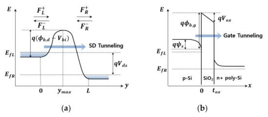
Figure 1.
Representation of the energy barrier profile (a) along the y-axis in the source-drain direction and (b) along the x-axis in the channel-gate direction.
The spectral density of shot noise is expressed by the Fano factor as a function of frequency where or corresponds to the source-drain or channel-gate current. The microscopic mechanisms responsible for shot noise have been associated with a sequential tunneling (ST) through the potential barrier [36,37]. The sequential tunneling model is described by the interaction of carriers, resulting in other tunneling events due to the potential fluctuation [23,36,37]. The electron transport is governed by the total number of carriers between the left reservoir and barrier . Using the Langevin Equation for the number fluctuation and making a Fourier transform, the spectral density of shot noise is obtained as [23,36,37]
where is the average number of and and are the characteristic times related to due to the current fluctuations through the left and right reservoirs, respectively. If the flow rate of injected carriers from the left in the single barrier is independent of , the characteristic times and given in Equation (16) are represented by the derivatives of carrier flow to the left and to the right , respectively. By using the Landauer formula and introducing the ballistic efficiency , , and take the expressions [11,36,37,38]
where is the Planck’s constant and and 3 are the source-drain and the channel-gate tunneling, respectively. and are the Fermi–Dirac distribution functions of the transversal energy and longitudinal energy at the left and right reservoirs, respectively. The derivatives of Equations (18) and (19) with respect to lead to the expression (= 1 for L and = 2 for R)
For the source-drain tunneling, . By differentiating Equation (14) with respect to and synthesizing all electrostatic effects in a geometrical gate capacitance , the derivatives of the first term in Equation (21) become
where , , , and are the quantum capacitances of the gate, source and drain, respectively, and are the Fermi energy of the source and the drain, respectively, and is the 2D density-of-states (DOS) in the channel [14,38].
In the case of the channel-gate tunneling through the oxide layer, the derivatives are obtained from Equations (15) and (20) as
where , , , and [23]. Note that the set of Equations (16), (17) and (20)–(25) provide the analytical formulation of the shot noise as a function of the applied voltages.
3. Artificial Neural Network Model
Figure 2 shows a neural-based small-signal equivalent circuit of a quasi-ballistic MOSFET including the drain, gate, correlation noise model, and conductance model, as well as the shot noise due to the gate and source-drain tunneling current. The capacitor and are the capacitance of the gate-source and the gate-drain overlap, respectively. The gate resistance consists of the distributed gate electrode resistance and the non-quasistatic (NQS) distributed channel resistance [39]. At a high frequency operation in GHz range of devices, the channel transit time is comparable to the input signals, and hence the NQS distributed gate resistance should be included in the equivalent circuit [39,40]. The proposed ANN model has been developed by using a network associated with the radial basis function (RBF). The RBF neural network shows advantages with respect to the multilayer perceptron (MLP), since it has a simpler structure and a much faster training process [27,41,42,43]. The RBF neural network is a universal approximator which can solve extremely nonlinear problems with a high degree of accuracy [43]. The RBF neural network structure consists of three layers. The input and hidden layers in the RBF neural network include input signals and radial basis transfer functions, respectively, and the output layer performs the linear combination of weighted RBF outputs.
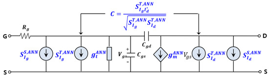
Figure 2.
Neural-based small-signal equivalent circuit model of a quasi-ballistic MOSFET for high frequency noise analysis. The model describes the drain, gate, correlation noise source, and conductance as well as the gate and drain shot noise source.
3.1. RBF-ANN and RBF-DANN
The RBF-ANN input to the transfer function is the distance between the input , and its weight multiplied by the bias as follows
where is the weight for the kth neuron and jth input, and is the bias for the kth neuron. The transfer function for a radial basis neuron in the hidden layer is Gaussian function
where the weight performs the Gaussian center and the bias acts as variance. For a given input and , the input-output mapping for the drain current and the gate leakage current can be computed by [27]
where , is the weight for the kth neurons of the output layer, and is the bias for the output layer.
Output conductance () and transconductance () can be obtained by the differential of Equation (28) with respect to the input , , and the RBF-DANN (Differential ANN) function for becomes
For neural modeling of shot noise, the expression of RBF neural network for the Fano factor () in Equation (16) is obtained as
The complete shot noise for is expressed by using Equations (28) and (30) as follows
3.2. RBF-IANN
The ANN model for the thermal noise of the drain current, the induced gate current, and the correlation is obtained by training the integrand function of Equations (8), (11), and (12) describing the noise source The network input to the transfer function is , , , and , and the integrand function with is expressed as [27]
With the use of Gaussian integral approximation, the noise integral is parameterized by the error function as
The integral Equation (33) can be approximated by the hyperbolic tangent function, and RBF-IANN (Integration of ANN) function is given by
This neural approach can be extended to model the high-dimensional input vector, including the channel length and temperature, to illustrate the capability of the PINN framework.
3.3. ANN Structure for Noise Performance
With knowledge of the basic noise sources, it is possible to estimate the high frequency noise performance, as shown in Figure 3. The ANN noise modeling structure consists of the neural model of noise sources and an improved noise equivalent circuit model. The individual elements in the equivalent circuit are described in Figure 2. For the prediction of noise performance, the noise parameters such as the minimum noise figure , the noise resistance , and the optimum source admittance are estimated by using , , , and as follows [2,3,4,5,6,7,9]
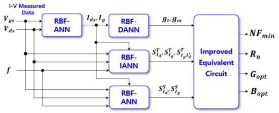
Figure 3.
ANN (artificial neural networks) -based noise modeling for the estimation of HF (high frequency) noise performance.
To derive , , , and , all the noise sources in Figure 2 are first transferred to the input of noise-free circuit as a series noise voltage and a shunt noise current [2,9]. Next, the correlation matrix is obtained in its chain form, leading to the expressions [2,9]
where , and and are the neural models of Y-parameters, including the conductance due to the gate tunneling current .
4. Model Verification
In order to measure I-V and noise characteristics, devices are fabricated with a remote plasma nitride oxide and standard processing techniques on p-Si substrate with n+ poly-Si gates. The noise and scattering parameters of a 28 nm device ( are measured using the HP8970 (HP Inc., Palo Alto, CA, USA) noise figure tester in the frequency range from 2GHz to 10GHz, in conjunction with the HP8510C(HP Inc., Palo Alto, CA, USA) network analyzer and the HP4156(HP Inc., Palo Alto, CA, USA) parameter analyzer. Noise correlation matrix of admittance representation is constructed from the measured noise and scattering parameters to calculate the noise sources. From the measured scattering-parameters, Y-parameters are obtained, and the parameters of the equivalent circuit are carefully extracted by using the open and short de-embedding techniques [2,3,4]. To check the accuracy of measured noise data, is measured using scattering parameter setup, and then extrinsic drain current noise is compared with ). It is confirmed that and are nearly equal over all the measured frequencies and different gate voltages, demonstrating the accuracy of noise measurement [4]. The noise figure is extracted after eliminating the noise contribution from the parasitic resistances [2].
Figure 4 shows the comparison of measured data with the results obtained using the RBF-DANN model for the drain transconductance and the gate tunnelling conductance. To build the RBF-DANN models, the measured I-V data as a function of , are selected to train the network, and a different subset of measured data is used to test the trained RBF-DANN. The network has three layers and five neurons in the RBF-DANN, and the training processes use optimized variances for different voltages. For the implementation of RBF-ANN models for the shot noise, the network is a trained numerical data set, as shown in Figure 5. Numerical calculations are performed by using Equations (16) and (17) with = 2.6 eV , , , , , for , and for .
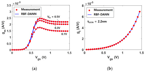
Figure 4.
Comparison of measured data with the results obtained using the RBF-DANN (radial basis function-differential artificial neural networks) model for (a) the drain transconductance and (b) the gate tunnelling conductance .
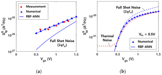
Figure 5.
Comparison of measured and numerical data with the results obtained using the RBF-DANN model for (a) the gate current shot noise and (b) the drain current shot noise.
It is found in Figure 5a that large enhancement in the gate shot noise has a good agreement with the experimental results. This is generated by the positive correlation between tunneling into the gate due to the interplay between the DOS and electrostatics [15,23]. For moderately high voltages in the inversion region, as can be seen in Figure 5b, is so low that injection noise from the left reservoir is dominant, leading to the noise suppression () in the drain shot noise [1,14,15,16,17,18]. This observation suggests that at , the major noise source shifts from thermal noise to shot noise. The dominance of the potential barrier in quasi-ballistic MOSFETs in strong inversion leads to shot noise, and in consequence, the noise power will show weak temperature dependence owing to a non-thermal effect [44,45]. For low gate voltages below 0.5 V, however, the noise power acts as the thermal noise with temperature dependence, as expected from Equation (8) [44,45].
Figure 6 shows the comparison of numerical results with measured data and the RBF-IANN model for the thermal drain current noise. Figure 6a compares the measured data with numerical results of thermal drain current noise for various voltages, showing a good agreement. As shown in Figure 6b, the RBF-IANN simulation results are further compared with numerical data for the integrand of the drain current noise of Equation (8). The RBF-IANN consists of the same structure as the RBF-DANN in the neural network. Note that the RBF-IANN has an input parameter of the normalized spatial distribution of the local current noise source , incorporating the physical origin of the high frequency [7]. Numerical calculations are performed with , , , .
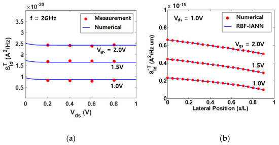
Figure 6.
(a) Comparison of measured data with numerical results obtained using the analytical model of Equation (7) for the thermal drain current noise and (b) the comparison of numerical data with the results obtained using the RBF-IANN model for the integrand of the thermal drain current noise of Equation (7).
The neural network is trained using these numerical data, leading to an accurate prediction of the RBF-IANN of the drain current noise for different voltages in Figure 7a–c, which show the comparison of numerical data with the results obtained using the RBF-IANN model for the induced gate current noise and the drain-gate correlation noise, respectively. The induced gate noise and the drain-gate correlation noise are also obtained by using a similar methodology to neural modelling of the drain current noise. The inset of Figure 7 shows a plot of the relative error values, which are less than 0.5%. As demonstrated in Figure 7, the RBF-IANN model has strong capability to perfectly predict the thermal noise characteristics for various input parameters.
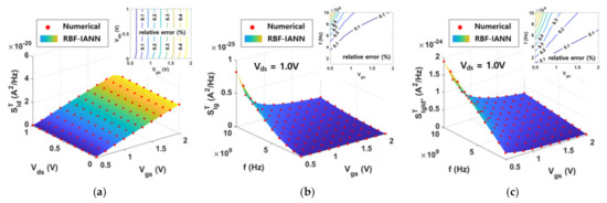
Figure 7.
Comparison of numerical data with results obtained using the RBF-IANN model for (a) the thermal drain current noise, (b) the induced gate current noise, and (c) the drain-gate correlation noise.
Figure 8 shows the noise parameter prediction with the ANN-based equivalent circuit model in 28nm scale quasi-ballistic MOSFETs. The solid line represents the prediction by including the gate and drain shot noise sources of Equation (31), and the dashed line represents the prediction by ignoring the shot noise sources. This figure clearly shows the significant impact of the gate and drain shot noise on the noise parameters, and it demonstrates the good capability of the ANN-based equivalent circuit model in predicting the noise performance.
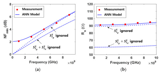
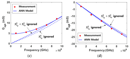
Figure 8.
Comparison of the ANN-based model with measured data for the noise parameters at for , , and (a) the minimum noise figure , (b) the noise resistance , (c) the optimum source conductance , and (d) optimum source susceptance .
5. Conclusions
The physics-informed neural network model for the high frequency noise performance, which takes into account the gate and drain shot noise effects, is proposed and verified by measured noise data for quasi-ballistic MOSFETs. The proposed model combines the equivalent noise circuit and ANN-based noise models to achieve higher accuracy. The ANN-based noise models are trained by using theoretical data for the thermal drain current noise, induced gate noise, its correlation noise, and drain and gate shot noise which incorporate the physical origin of high frequency. It is shown that the shot noise, due to the gate and source-drain tunneling current, significantly affects the noise parameters, demonstrating the need for a new modeling approach. The validity of the new approach is proved by the comparison with measured noise parameters up to 10GHz for various voltages. The proposed model provides physically feasible predictions and can be more readily generalized to the noise modeling of 10nm scale ballistic MOSFETs.
Funding
This work was supported by the National Research Foundation of Korea (NRF) grant funded by the Korea government (MSIT) (No. 2019R1F1A1050640).
Conflicts of Interest
The author declares no conflict of interest.
References
- Chen, X.; Chen, C.H.; Lee, R. Fast evaluation of the high-frequency channel noise in nanoscale MOSFETs. IEEE Trans. Electron. Devices 2018, 65, 1502–1508. [Google Scholar] [CrossRef]
- Deen, M.J.; Chen, C.H.; Asgaran, S.; Rezvani, G.A.; Tao, J.; Kiyota, Y. High frequency noise of modern MOSFETs: Compact modeling and measurement issues. IEEE Trans. Electron. Devices 2006, 53, 2062–2081. [Google Scholar] [CrossRef]
- Han, K.; Gil, J.; Song, S.S.; Han, J.; Shin, H.; Kim, C.K.; Lee, K. Complete high-frequency thermal noise modeling of short-channel MOSFETs and design of 5.2GHz low noise amplifier. IEEE J. Solid-State Circuits 2005, 40, 726–734. [Google Scholar]
- Han, K.; Shin, H.; Lee, K. Analytical drain thermal noise current model valid for deep submicron MOSFETs. IEEE Trans. Electron. Devices 2004, 51, 261–269. [Google Scholar] [CrossRef]
- Asgaran, S.; Deen, M.J.; Chen, C.H. Analytical modeling of MOSFETs channel noise and noise parameters. IEEE Trans. Electron. Devices. 2004, 51, 2109–2114. [Google Scholar] [CrossRef]
- Jeon, J.; Kim, Y.; Kang, M. Investigation of the induced gate noise of nanoscale MOSFETs in the very high frequency region. Semicond. Sci. Technol. 2016, 31, 065004. [Google Scholar] [CrossRef]
- Jeon, J.; Yun, Y.; Kim, J.; Park, B.G.; Lee, J.D.; Shin, H. On the characteristics and spatial dependence of channel thermal noise in nanoscale metal oxide semiconductor field effect transistors. Jpn. J. Appl. Phys. 2008, 47, 2636–2640. [Google Scholar] [CrossRef]
- Ohmori, K.; Amakawa, S. Direct white noise characterization of short-channel MOSFETs. IEEE Trans. Electron. Devices 2021, 68, 1478–1482. [Google Scholar] [CrossRef]
- Jeon, J.; Kang, M. Shot noise effect on noise source and noise parameter of 10-nm-scale quasi-ballistic n-/p-type MOS devices. Jpn. J. Appl. Phys. 2016, 55, 054102. [Google Scholar] [CrossRef]
- Naveh, Y.; Likharev, K.K. Modeling of 10nm-scale ballistic MOSFET’s. IEEE Electron Device Lett. 2000, 21, 242–244. [Google Scholar] [CrossRef]
- Lin, Y.K.; Duarte, J.P.; Kushwaha, P.; Agarwal, H.; Chang, H.L.; Sachid, A.; Salahuddin, S.; Hu, C. Compact modeling source-to-drain tunneling in sub-10nm GAA FinFET with industry standard model. IEEE Trans. Electron. Devices 2017, 64, 3576–3581. [Google Scholar] [CrossRef]
- Hiblot, G.; Rafhay, Q.; Boeuf, F.; Ghibaudo, G. Analytical relationship between subthreshold swing of thermionic and tunneling currents. Electron. Lett. 2014, 50, 1745–1747. [Google Scholar] [CrossRef]
- Cheng, H.; Liu, T.; Zhang, C.; Yang, Z.; Liu, Z.; Nakazato, K.; Zhang, Z. Nanowire gate-all-around MOSFETs modeling: Ballistic transport incorporating the source-to-drain tunneling. Jpn. J. Appl. Phys. 2020, 59, 1–9. [Google Scholar] [CrossRef]
- Mugnaini, G.; Iannaccone, G. Channel noise modeling of nanoMOSFETs in a partially ballistic transport regime. J. Comput. Electron. 2006, 5, 91–95. [Google Scholar] [CrossRef]
- Iannaccone, G.; Betti, A.; Fiori, G. Suppressed and enhanced shot noise in one dimensional field-effect transistors. J. Comput. Electron. 2015, 14, 94–106. [Google Scholar] [CrossRef]
- Iannaccone, G. Analytical and numerical investigation of noise in nanoscale ballistic field effect transistors. J. Comput. Electron. 2004, 3, 199–202. [Google Scholar] [CrossRef][Green Version]
- Jia, X.; He, L. Research of shot noise based on realistic nano-MOSFETs. AIP Adv. 2017, 7, 055202. [Google Scholar] [CrossRef]
- Spathis, C.; Birbas, A.; Georgakopoulou, K. Semi-classical noise investigation for sub-40nm metal-oxide-semiconductor field-effect transistors. AIP Adv. 2015, 5, 087114. [Google Scholar] [CrossRef]
- Ranuarez, J.C.; Deen, M.J.; Chen, C.H. A review of gate tunneling current in MOS devices. Microelectron. Rel. 2006, 46, 1939–1956. [Google Scholar] [CrossRef]
- Clerc, R.; O’Sullivan, P.; McCarthy, K.G.; Ghibaudo, G.; Pananakakis, G.; Mathewson, A. A physical compact model for direct tunneling from NMOS inversion layers. Solid-State Electron. 2001, 45, 1705–1716. [Google Scholar] [CrossRef]
- Gehring, A.; Selberherr, S. Modeling of tunneling current and gate dielectric reliability for nonvolatile memory devices. IEEE Trans. Device Mater. Reliab. 2004, 4, 306–319. [Google Scholar] [CrossRef]
- Mao, L.F.; Li, X.J.; Wang, Z.O.; Wang, J.Y. The gate leakage current in graphene field-effect transistor. IEEE Electron Device Lett. 2008, 29, 1047–1049. [Google Scholar] [CrossRef]
- Lee, J.; Bosman, G.; Green, K.R.; Ladwig, D. Noise model of gate-leakage current in ultrathin oxide MOSFETs. IEEE Trans. Electron. Devices 2003, 50, 2499–2506. [Google Scholar]
- Manghisoni, M. Gate current noise in ultrathin oxide MOSFETs and its impact on the performance of analog front-end circuits. IEEE Trans. Nucl. Sci. 2008, 55, 2399–2407. [Google Scholar] [CrossRef]
- Huang, A.D.; Zhong, Z.; Wu, W.; Guo, Y.X. An artificial neural network-based electrothermal model for GaN HEMTs with dynamic trapping effects consideration. IEEE Trans. Microw. Theory Technol. 2016, 64, 2519–2528. [Google Scholar] [CrossRef]
- Li, X.; Gao, J.; Boeek, G. Microwave nonlinear device modeling by using an artificial neural network. Semicond. Sci. Technol. 2006, 21, 833–840. [Google Scholar] [CrossRef]
- Lee, J. Physics-guided neural modeling for low-dimensional thermoelectric module. IEEE Electron Device Lett. 2019, 40, 1812–1815. [Google Scholar] [CrossRef]
- Li, M.; Irsoy, O.; Cardie, C.; Xing, H.G. Physics-inspired neural networks for efficient device compact modeling. IEEE J. Explor. Solid-State Compu. Devices Circuits 2016, 2, 44–49. [Google Scholar] [CrossRef]
- Zhang, L.; Chan, M. Artificial neural network design for compact modeling of generic transistors. J. Comput. Electron. 2017, 16, 825–832. [Google Scholar] [CrossRef]
- Jarndal, A. On neural network based electro- thermal modeling of GaN devices. IEEE Access. 2019, 7, 94205–94214. [Google Scholar] [CrossRef]
- Wu, T.; Guo, J. Speed up quantum transport device simulation on ferroelectric tunnel junction with machine learning methods. IEEE Trans. Electron. Devices 2020, 67, 5229–5235. [Google Scholar] [CrossRef]
- Wang, J.; Kim, Y.H.; Ryu, J.; Jeong, C.; Choi, W.; Kim, D. Artificial neural network-based compact modeling methodology for advanced transistors. IEEE Trans. Electron. Devices 2021, 68, 1318–1325. [Google Scholar] [CrossRef]
- Mehta, K.; Wong, H.Y. Prediction of FinFET current-voltage and capacitance-voltage curves using machine learning with autoencoder. IEEE Electron Device Lett. 2021, 42, 136–139. [Google Scholar] [CrossRef]
- Carrillo-Nunez, H.; Dimitrova, N.; Asenov, A.; Georgiev, V. Machine learning approach for predicting the effect of statistical variability in Si junction-less nanowire transistors. IEEE Electron Device Lett. 2019, 40, 1366–1369. [Google Scholar] [CrossRef]
- Pregaldiny, F.; Lallement, C.; van Langevelde, R.; Mathiot, D. An advanced explicit surface potential model physically accounting for the quantization effects in deep-submicron MOSFETs. Solid-State Electron. 2004, 48, 427–435. [Google Scholar] [CrossRef]
- Aleshkin, V.Y.; Reggiani, L. Electron transport and shot noise in double-barrier resonant diodes: The role of Pauli and Coulomb correlations. Phys. Rev. B. 2001, 64, 245333. [Google Scholar] [CrossRef]
- Aleshkin, V.Y.; Reggiani, L. Comparative analysis of sequential and coherent tunneling in resonant diodes. Phys. Rev. B. 2006, 73, 165320. [Google Scholar] [CrossRef]
- Marin, E.G.; Bader, S.J.; Jena, D. A new holistic model of 2-D semiconductor FETs. IEEE Trans. Electron. Devices 2018, 65, 1239–1245. [Google Scholar] [CrossRef]
- Cheng, Y.; Denn, J.M.; Chen, C.H. MOSFET modeling for RF IC design. IEEE Trans. Electron. Devices 2005, 52, 1286–1303. [Google Scholar] [CrossRef]
- Cheng, Y.; Matloubian, M. High frequency characterization of gate resistance in RF MOSFETs. IEEE Electron Device Lett. 2001, 22, 98–100. [Google Scholar] [CrossRef]
- Weatherspoon, M.H.; Martinez, H.A.; Langoni, D.; Foo, S.Y. Small-signal modeling of microwave MESFETs using RBF-ANNs. IEEE Trans. Instrum. Meas. 2007, 56, 2067–2072. [Google Scholar] [CrossRef]
- Djeffal, F.; Dibi, Z.; Hafiane, M.L.; Arar, D. Design and simulation of a nanoelectronic DG MOSFET current source using artificial neural networks. Mater. Sci. Eng. C 2007, 27, 1111–1116. [Google Scholar] [CrossRef]
- Wu, Y.; Wang, H.; Zhang, B.; Du, K.L. Using radial basis function networks for function approximation and classification. ISRN Appl. Math. 2012, 2012, 1–34. [Google Scholar] [CrossRef]
- Navid, R.; Jungemann, C.; Lee, T.H.; Dutton, R.W. High-frequency noise in nanoscale metal oxide semiconductor field effect transistors. J. Appl. Phys. 2007, 101, 124501. [Google Scholar] [CrossRef]
- Wang, J. Bias non-conservation characteristics of drain current noise of 40nm n-MOSFETs in high-frequency band. Electron. Lett. 2017, 53, 1671–1672. [Google Scholar] [CrossRef]


Publisher’s Note: MDPI stays neutral with regard to jurisdictional claims in published maps and institutional affiliations. |
© 2021 by the author. Licensee MDPI, Basel, Switzerland. This article is an open access article distributed under the terms and conditions of the Creative Commons Attribution (CC BY) license (https://creativecommons.org/licenses/by/4.0/).