
Dimming Techniques Focusing on the Improvement in Luminous Efficiency for High-Brightness LEDs †


Abstract
:
1. Introduction
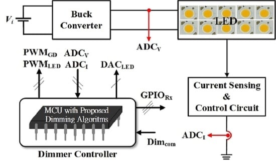
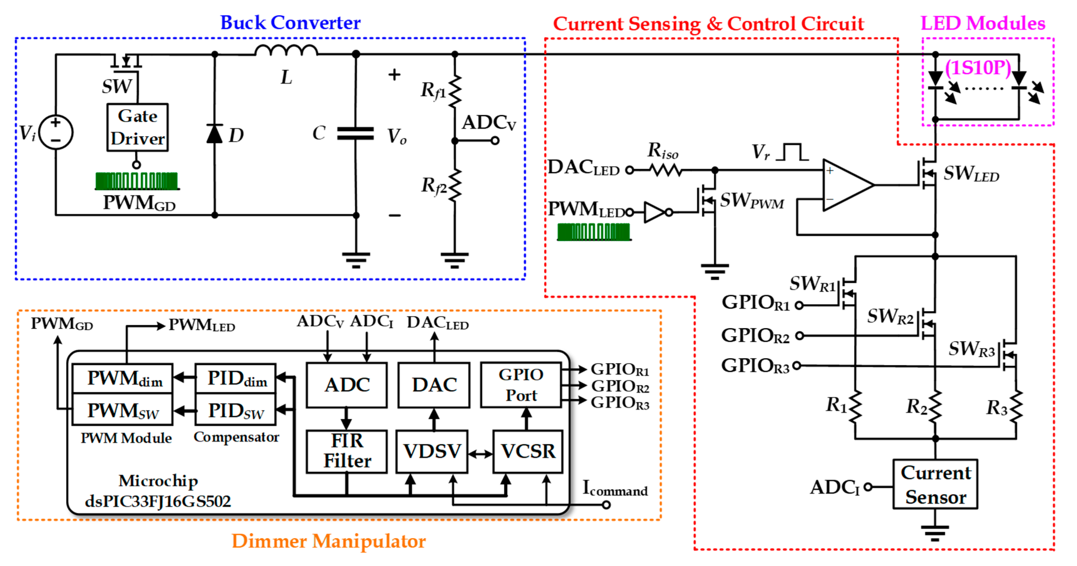
2. Configuration of the Studied LED Driver
2.1. Buck Converter and Design Consideration
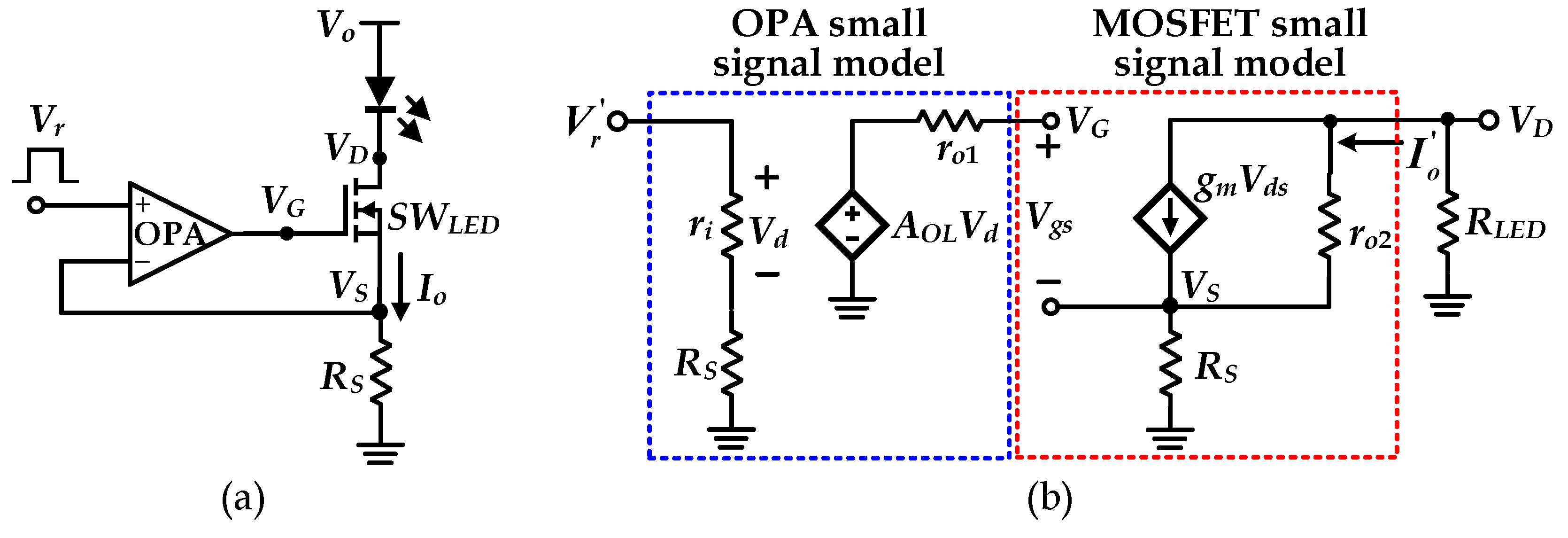
2.2. Linear Current Control Circuit
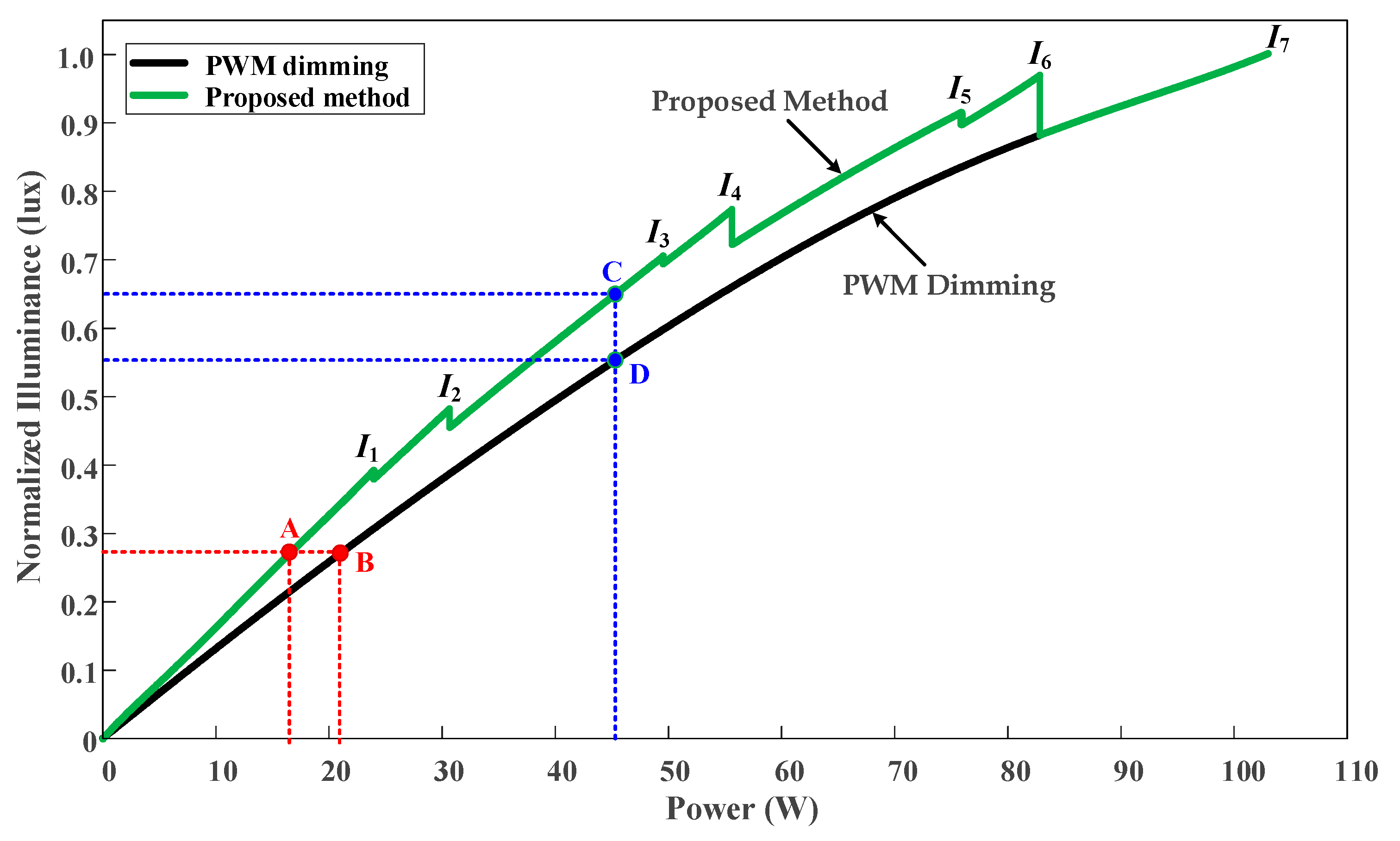
3. Proposed Dimming Control Method
3.1. The Dimming with VCSR
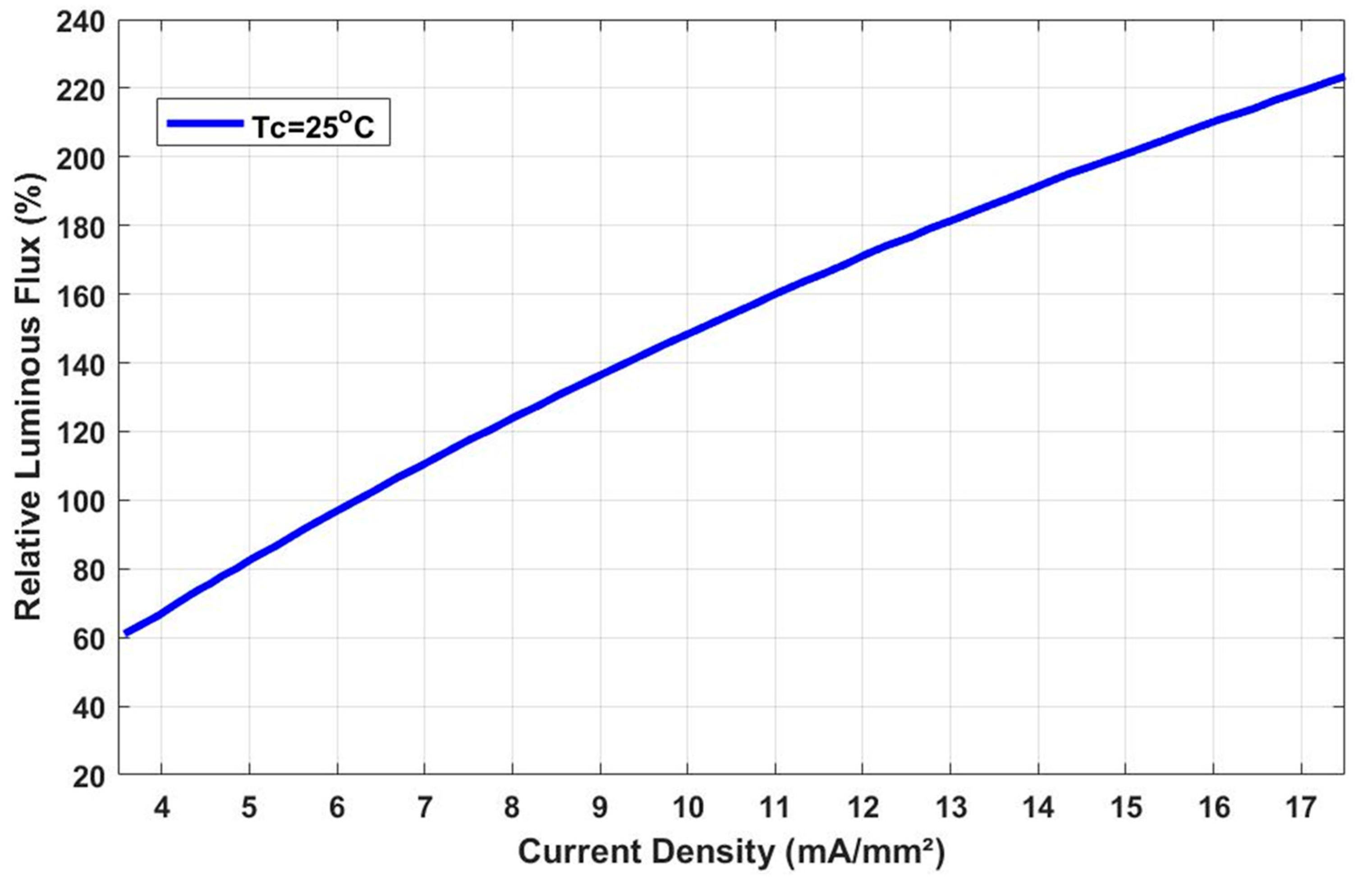
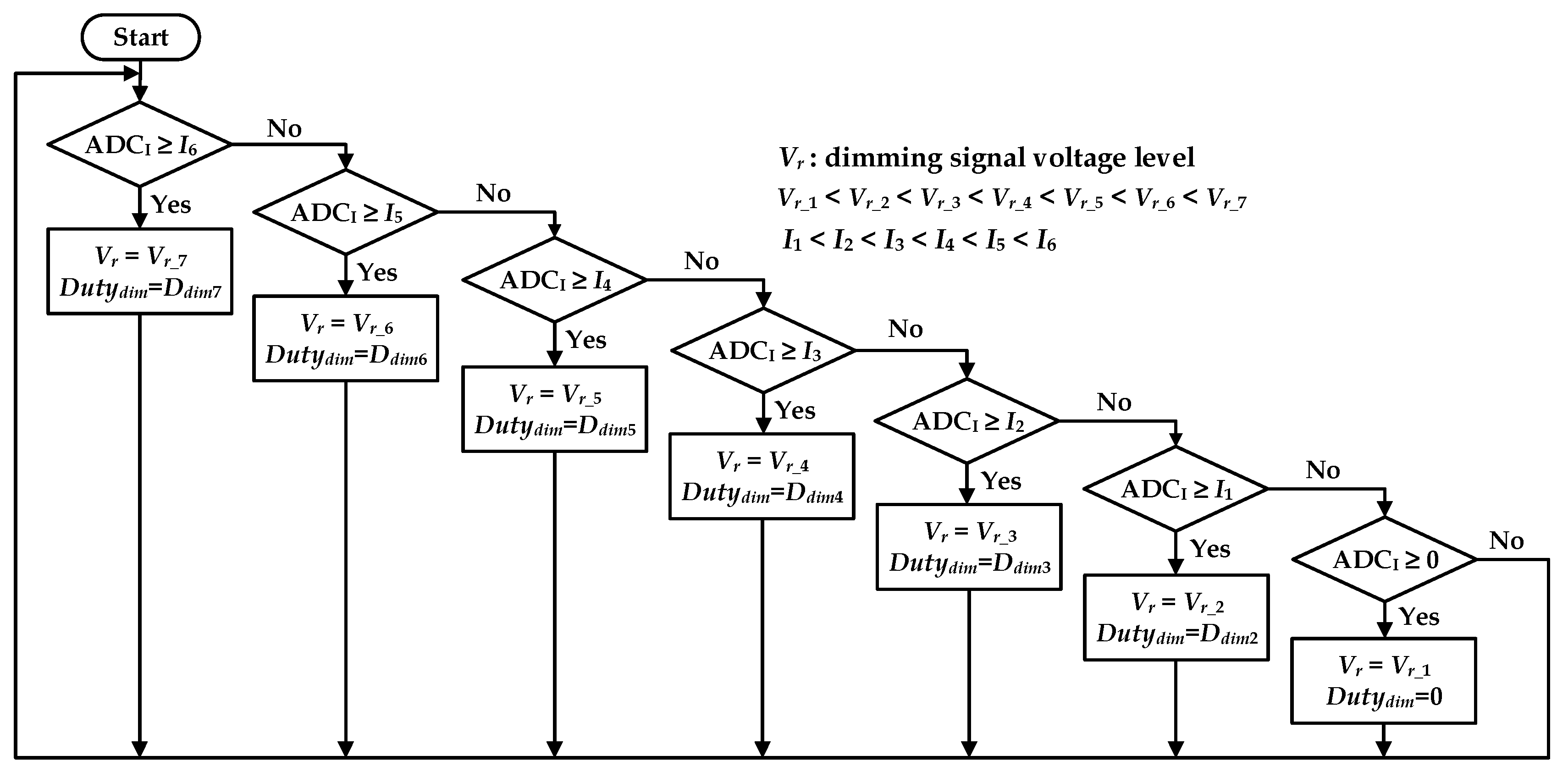
3.2. The Dimming with VDSV
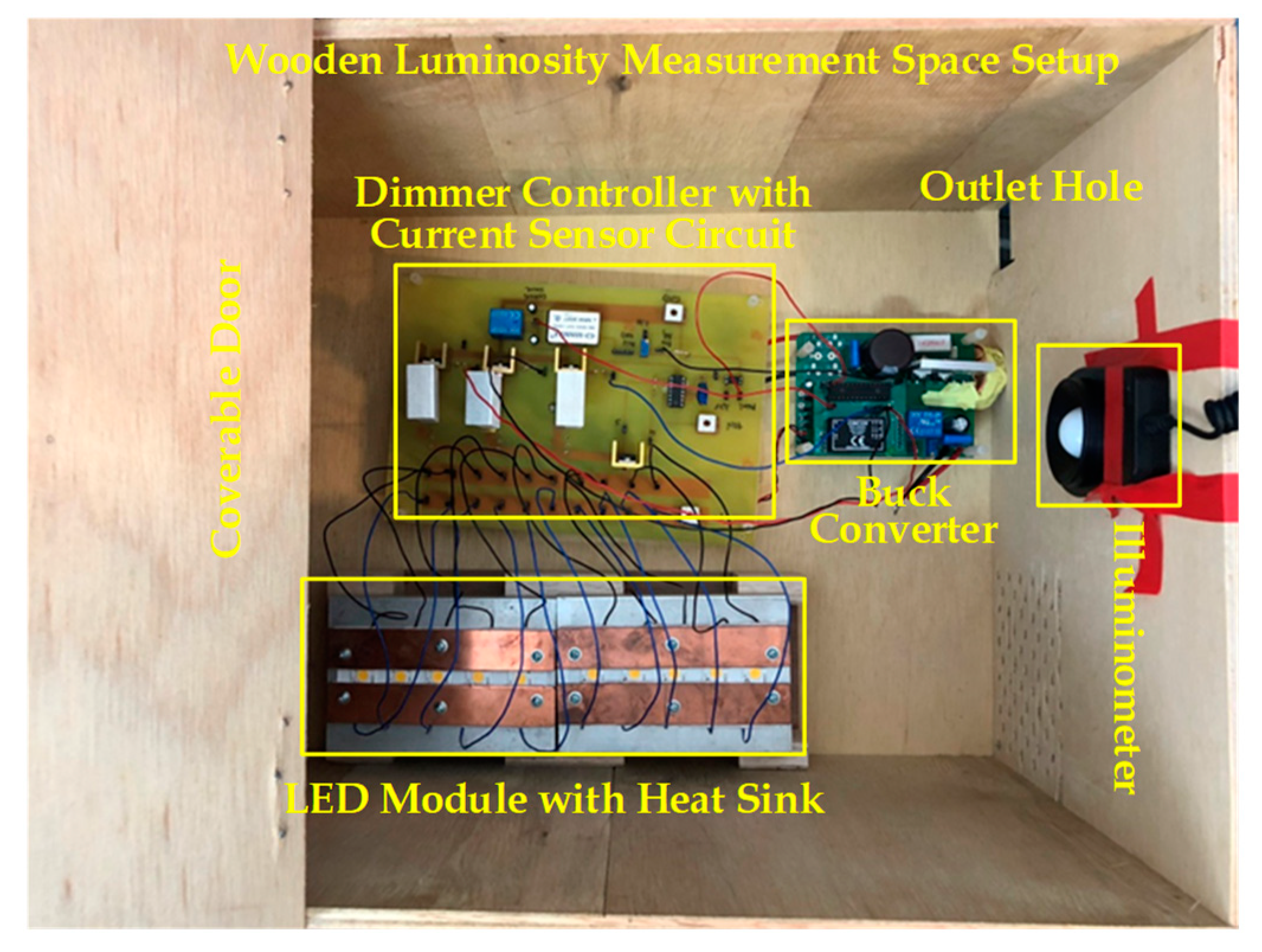
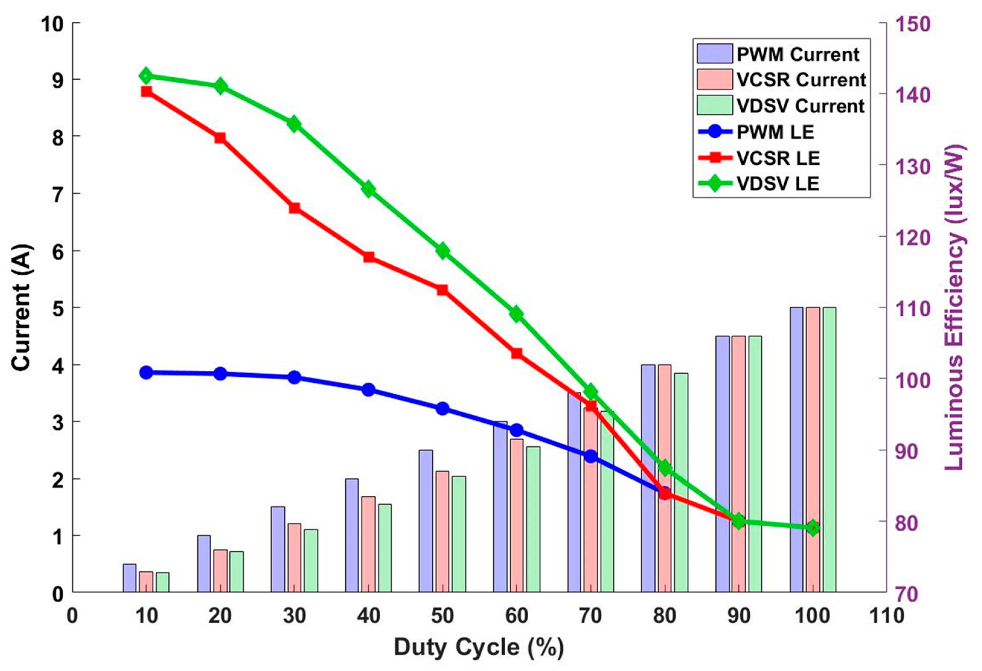
4. Experimental Results
5. Conclusions
Author Contributions
Funding
Conflicts of Interest
References
- Ponce-Silva, M.; Salazar-Pérez, D.; Rodríguez-Benítez, O.M.; Vela-Valdés, L.G.; Claudio-Sánchez, A.; De León-Aldaco, S.E.; Cortés-García, C.; Saavedra-Benítez, Y.I.; Lozoya-Ponce, R.E.; Aquí-Tapia, J.A. Flyback Converter for Solid-State Lighting Applications with Partial Energy Processing. Electronics 2021, 10, 60. [Google Scholar] [CrossRef]
- Xu, H.; An, F.; Wen, S.; Yan, Z.; Guan, W. Three-Dimensional Indoor Visible Light Positioning with a Tilt Receiver and a High Efficient LED-ID. Electronics 2021, 10, 1265. [Google Scholar] [CrossRef]
- Schirripa Spagnolo, G.; Leccese, F. LED Rail Signals: Full Hardware Realization of Apparatus with Independent Intensity by Temperature Changes. Electronics 2021, 10, 1291. [Google Scholar] [CrossRef]
- Li, S.; Tan, S.; Lee, C.K.; Waffenschmidt, E.; Hui, S.Y.; Tse, C.K. A Survey, Classification, and Critical Review of Light-Emitting Diode Drivers. IEEE Trans. Power Electron. 2016, 31, 1503–1516. [Google Scholar] [CrossRef] [Green Version]
- Vasilopoulou, M.; Yusoff, M.; Daboczi, M.; Conforto, J.; Gavim, A.E.; da Silva, W.J.; Macedo, A.G.; Soultati, A.; Pistolis, G.; Schneider, F.K.; et al. High Efficiency Blue Organic Light-Emitting Diodes with Below-Bandgap Electroluminescence. Nat. Commun. 2021, 12, 4868. [Google Scholar] [CrossRef] [PubMed]
- Vasilopoulou, M.; Kim, H.P.; Kim, B.S.; Papadakis, M.; Gavim, A.E.; Macedo, A.G.; da Silva, W.J.; Schneider, F.K.; Teridi, M.A.; Coutsolelos, A.G.; et al. Efficient Colloidal Quantum Dot Light-Emitting Diodes Operating in the Second Near-infrared Biological Window. Nat. Photon. 2020, 14, 50–56. [Google Scholar] [CrossRef]
- Yuan, F.; Zheng, X.; Johnston, A.; Wang, Y.K.; Zhou, C.; Dong, Y.; Chen, B.; Chen, H.; Fan, J.Z.; Sharma, G.; et al. Color-Pure Red Light-Emitting Diodes Based on Two-Dimensional Lead-Free Perovskites. Sci. Adv. 2020, 6, eabb0253. [Google Scholar] [CrossRef]
- Wang, Y.K.; Yuan, F.; Dong, Y.; Li, J.Y.; Johnston, A.; Chen, B.; Saidaminov, M.I.; Zhou, C.; Zheng, X.; Hou, Y.; et al. All-Inorganic Quantum-Dot LEDs Based on a Phase-Stabilized α-CsPbI3 Perovskite. Angew. Chem. Int. Ed. 2021, 60, 16164–16170. [Google Scholar] [CrossRef] [PubMed]
- Kim, J.U.; Park, I.S.; Chan, C.-Y.; Tanaka, M.; Tsuchiya, Y.; Nakanotani, H.; Adachi, C. Nanosecond-time-scale delayed fluorescence molecule for deep-blue OLEDs with small efficiency rolloff. Nat. Commun. 2020, 11, 1–8. [Google Scholar] [CrossRef] [Green Version]
- Chan, C.-Y.; Tanaka, M.; Lee, Y.-T.; Wong, Y.-W.; Nakanotani, H.; Hatakeyama, T.; Adachi, C. Stable pure-blue hyperfluorescence organic light-emitting diodes with high-efficiency and narrow emission. Nat. Photon. 2021, 15, 203–207. [Google Scholar] [CrossRef]
- Pinti, F.; Belli, A.; Palma, L.; Gattari, M.; Pierleoni, P. Validation of Forward Voltage Method to Estimate Cracks of the Solder Joints in High Power LED. Electronics 2020, 9, 920. [Google Scholar] [CrossRef]
- Pirc, M.; Caserman, S.; Ferk, P.; Topič, M. Compact UV LED Lamp with Low Heat Emissions for Biological Research Applications. Electronics 2019, 8, 343. [Google Scholar] [CrossRef] [Green Version]
- Rachev, I.; Djamiykov, T.; Marinov, M.; Hinov, N. Improvement of the Approximation Accuracy of LED Radiation Patterns. Electronics 2019, 8, 337. [Google Scholar] [CrossRef] [Green Version]
- Raggiunto, S.; Belli, A.; Palma, L.; Ceregioli, P.; Gattari, M.; Pierleoni, P. An Efficient Method for LED Light Sources Characterization. Electronics 2019, 8, 1089. [Google Scholar] [CrossRef] [Green Version]
- Orem, P.M.; Vogt, K.T.; Graham, M.W.; Orem, F.M. Measuring Thermally-Driven LED Emissions via Voltage Modulation near Zero Bias. Electronics 2018, 7, 360. [Google Scholar] [CrossRef] [Green Version]
- Yamada, M.; Penning, J.; Schober, S.; Lee, K.; Elliott, C. Energy Savings Forecast of Solid-State Lighting in General Illumination Application; U.S. Department of Energy: Washington, DC, USA, 2019.
- Yan, Y.-H.; Cheng, H.-L.; Cheng, C.-A.; Chang, Y.-N.; Wu, Z.-X. A Novel Single-Switch Single-Stage LED Driver with Power Factor Correction and Current Balancing Capability. Electronics 2021, 10, 1340. [Google Scholar] [CrossRef]
- Yi, K.H. High Voltage, Low Current High-Power Multichannel LEDs LLC Driver by Stacking Single-Ended Rectifiers with Balancing Capacitors. Electronics 2020, 9, 529. [Google Scholar] [CrossRef] [Green Version]
- Ribas, J.; Quintana, P.J.; Cardesin, J.; Calleja, A.J.; Lopera, J.M. Closed Loop Control of a Series Class-E Voltage-Clamped Resonant Converter for LED Supply with Dimming Capability. Electronics 2019, 8, 1380. [Google Scholar] [CrossRef] [Green Version]
- Liu, T.; Liu, X.; He, M.; Zhou, S.; Meng, X.; Zhou, Q. Flicker-Free Resonant LED Driver with High Power Factor and Passive Current Balancing. IEEE Access 2021, 9, 6008–6017. [Google Scholar] [CrossRef]
- Liu, X.; Li, X.; Zhou, Q.; Xu, J. Flicker-Free Single Switch Multi-String LED Driver with High Power Factor and Current Balancing. IEEE Trans. Power Electron. 2019, 34, 6747–6759. [Google Scholar] [CrossRef]
- Castro, I.; Vazquez, A.; Arias, M.; Lamar, D.G.; Hernando, M.M.; Sebastian, J. A Review on Flicker-free AC–DC LED Drivers for Single-Phase and Three-Phase AC Power Grids. IEEE Trans. Power Electron. 2019, 34, 10035–10057. [Google Scholar] [CrossRef]
- Soh, M.Y.; Selvaraj, S.L.; Peng, L.; Yeo, K.S. 92.5% Average Power Efficiency Fully Integrated Floating Buck Quasi-Resonant LED Drivers Using GaN FETs. Electronics 2020, 9, 575. [Google Scholar] [CrossRef] [Green Version]
- Tung, N.T.; Tuyen, N.D.; Huy, N.M.; Phong, N.H.; Cuong, N.C.; Phuong, L.M. Design and Implementation of 150 W AC/DC LED Driver with Unity Power Factor, Low THD, and Dimming Capability. Electronics 2019, 9, 52. [Google Scholar] [CrossRef] [Green Version]
- Cheng, C.-A.; Chang, C.-H.; Cheng, H.-L.; Chang, E.-C.; Chung, T.-Y.; Chang, M.-T. A Single-Stage LED Streetlight Driver with Soft-Switching and Interleaved PFC Features. Electronics 2019, 8, 911. [Google Scholar] [CrossRef] [Green Version]
- Ribas, J.; Quintana, P.J.; Cardesin, J.; Calleja, A.J.; Lopez-Corominas, E. Single-Switch LED Post-Regulator Based on a Modified Class-E Resonant Converter with Voltage Clamp. Electronics 2019, 8, 798. [Google Scholar] [CrossRef] [Green Version]
- Garcia, J.; Saeed, S.; Quintana, P.; Cardesin, J.; Georgious, R.; Costa, M.A.D.; Camponogara, D. Optimization of a Series Converter for Low-Frequency Ripple Cancellation of an LED Driver. Electronics 2019, 8, 664. [Google Scholar] [CrossRef] [Green Version]
- Tahan, M.; Hu, T. Multiple String LED Driver with Flexible and High-Performance PWM Dimming Control. IEEE Trans. Power Electron. 2017, 32, 9293–9306. [Google Scholar] [CrossRef]
- Lv, X.; Loo, K.H.; Lai, Y.M.; Tse, C.K. Energy-Saving Driver Design for Full-Color Large-Area LED Display Panel Systems. IEEE Trans. Ind. Electron. 2014, 61, 4665–4673. [Google Scholar] [CrossRef]
- Yang, W.H.; Yang, H.A.; Huang, C.J.; Chen, K.H.; Lin, Y.H. A High-Efficiency Single-Inductor Multiple-Output Buck-Type LED Driver with Average Current Correction Technique. IEEE Trans. Power Electron. 2018, 33, 3375–3385. [Google Scholar] [CrossRef]
- Chen, H.; Zhou, X.; Lin, S.; Liu, J. Luminous Flux and CCT Stabilization of White LED Device with a Bi-level Driver. IEEE Photonics J. 2018, 10, 1–10. [Google Scholar]
- Ng, S.K.; Loo, K.H.; Ip, S.K.; Lai, Y.M.; Tse, C.K.; Mok, K.T. Sequential Variable Bi-level Driving Approach Suitable for Use in High-Color-Precision LED Display Panels. IEEE Trans. Ind. Electron. 2012, 59, 4637–4645. [Google Scholar] [CrossRef]
- Tan, S.C. General n-level Driving Approach for Improving Electrical-to-Optical Energy-Conversion Efficiency of Fast-Response Saturable Lighting Devices. IEEE Trans. Ind. Electron. 2010, 57, 1342–1353. [Google Scholar]
- Loo, K.H.; Lia, Y.M.; Tan, S.C.; Tse, C.K. On the Color Stability of Phosphor-Converted White LEDs under dc, PWM, and Bi-level Drive. IEEE Trans. Power Electron. 2012, 27, 974–984. [Google Scholar] [CrossRef]
- Cree Inc. XLamp LEDs. XLamp CXB1304 Datasheet 2018. Available online: https://cree-led.com/media/documents/ds-CXB1304.pdf (accessed on 21 July 2021).


| Buck Converter | |||
| Item | Design Spec. | Item | Part No. and Rating |
| Vi | 84 V | L | 1 mH |
| Vo | 23 V | C | 100 µF |
| Io | 5 A | D | STPS20150C (150 V/20 A) |
| Po | 115 W | SW | IPP030N10N3G (100 V/100 A) |
| fs (=1/Ts) | 35 kHz | - | - |
| Current Control Circuit | |||
| Item | Part No. and Rating | Item | Part No. and Rating |
| OPA | LM324 | SWLED | IPP200N25N3 (250 V/64 A) |
| SWR1,2.3 | IPP200N25N3 (250 V/64 A) | SWPWM | 2N7002 (60 V/0.3 A) |
| Level | R3 | R2 | R2//R3 | R1 | R1//R3 | R1//R2 | |
|---|---|---|---|---|---|---|---|
| Item | |||||||
| Power reduction | 14.5% | 16.5% | 14.9% | 16.7% | 10.9% | 6.1% | |
| Illumination boost | 17.0% | 18.7% | 15.6% | 16.5% | 9.0% | 3.6% | |
| Level | 0.33 V | 0.39 V | 0.72 V | 0.78 V | 1.1 V | 1.2 V | |
|---|---|---|---|---|---|---|---|
| Item | |||||||
| Power reduction | 20.4% | 20.9% | 16.6% | 17.1% | 12.3% | 13.5% | |
| Illumination boost | 24.9% | 24.0% | 17.5% | 16.5% | 9.3% | 8.5% | |
| Item | Average Power Reduction | Average Illumination Boost | |
|---|---|---|---|
| Method | |||
| VCSR | 13.17% | 11.17% | |
| VDSV | 17.08% | 13.66% | |
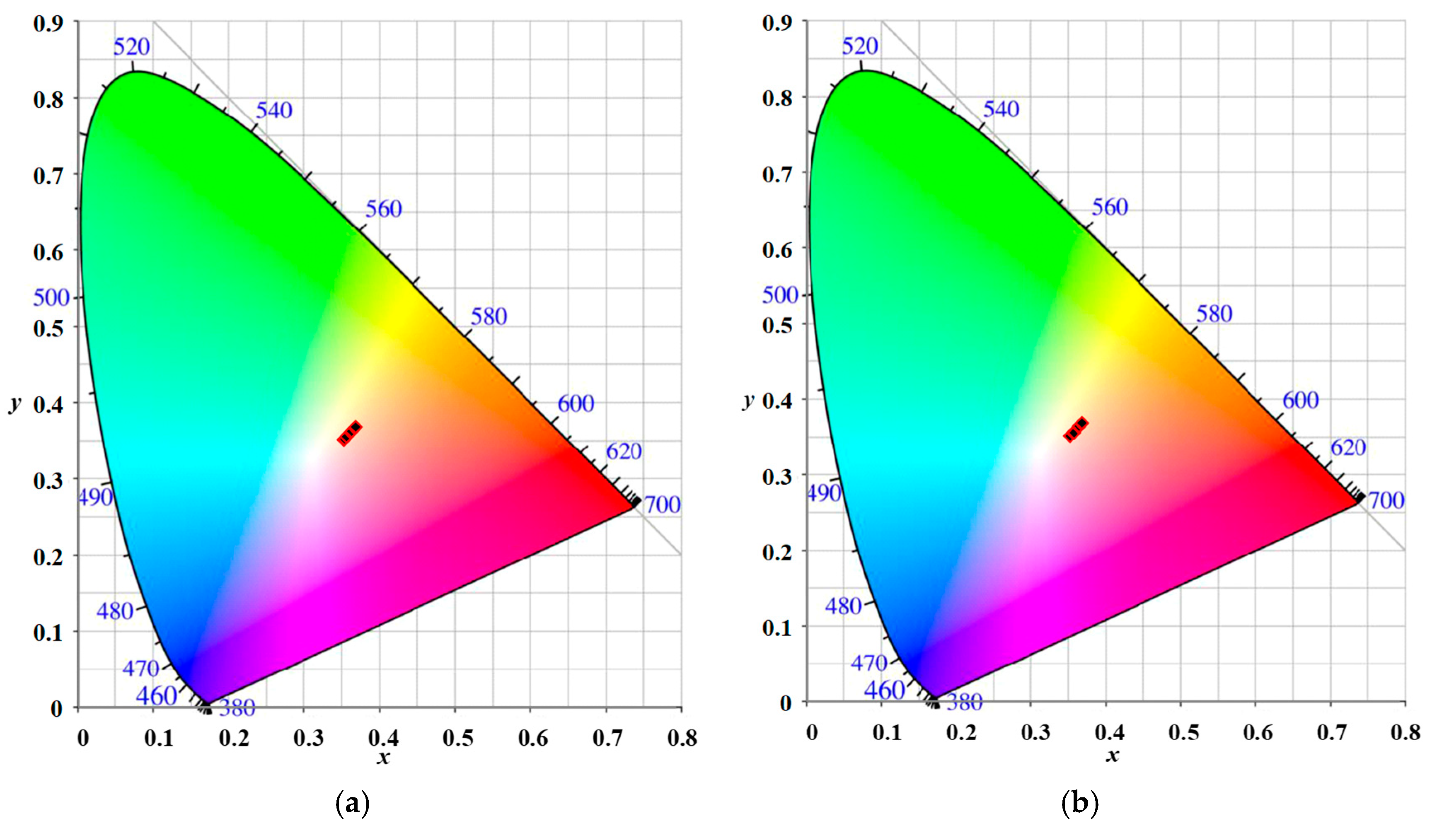
| Color Space | CIE 1931 | CIE 1976 | |||
|---|---|---|---|---|---|
| Method | Δx | Δy | Δu′ | Δv′ | |
| VCSR | 1.59 × 10⁻² | 1.68 × 10⁻² | 3.97 × 10⁻³ | 1.03 × 10⁻² | |
| VDSV | 1.61 × 10⁻² | 1.70 × 10⁻² | 4.04 × 10⁻³ | 1.04 × 10⁻² | |
Publisher’s Note: MDPI stays neutral with regard to jurisdictional claims in published maps and institutional affiliations. |
© 2021 by the authors. Licensee MDPI, Basel, Switzerland. This article is an open access article distributed under the terms and conditions of the Creative Commons Attribution (CC BY) license (https://creativecommons.org/licenses/by/4.0/).
Share and Cite
Ho, K.-C.; Wang, S.-C.; Liu, Y.-H. Dimming Techniques Focusing on the Improvement in Luminous Efficiency for High-Brightness LEDs. Electronics 2021, 10, 2163. https://doi.org/10.3390/electronics10172163
Ho K-C, Wang S-C, Liu Y-H. Dimming Techniques Focusing on the Improvement in Luminous Efficiency for High-Brightness LEDs. Electronics. 2021; 10(17):2163. https://doi.org/10.3390/electronics10172163
Chicago/Turabian StyleHo, Kun-Che, Shun-Chung Wang, and Yi-Hua Liu. 2021. "Dimming Techniques Focusing on the Improvement in Luminous Efficiency for High-Brightness LEDs" Electronics 10, no. 17: 2163. https://doi.org/10.3390/electronics10172163
APA StyleHo, K.-C., Wang, S.-C., & Liu, Y.-H. (2021). Dimming Techniques Focusing on the Improvement in Luminous Efficiency for High-Brightness LEDs. Electronics, 10(17), 2163. https://doi.org/10.3390/electronics10172163