Article

40 GHz VCO and Frequency Divider in 28 nm FD-SOI CMOS Technology for Automotive Radar Sensors

1
STMicroelectronics, 95121 Catania, Italy
2
STMicroelectronics, 20864 Agrate Brianza, Italy
*
Author to whom correspondence should be addressed.
Electronics 2021, 10(17), 2114; https://doi.org/10.3390/electronics10172114
Submission received: 29 June 2021 / Revised: 23 August 2021 / Accepted: 27 August 2021 / Published: 31 August 2021

Abstract

:
This paper presents a 40 GHz voltage-controlled oscillator (VCO) and frequency divider chain fabricated in STMicroelectronics 28 nm ultrathin body and box (UTBB) fully depleted silicon-on-insulator (FD-SOI) complementary metal-oxide–semiconductor (CMOS) process with eight metal layers back-end-of-line (BEOL) option. VCOs architecture is based on an LC-tank with p-type metal-oxide–semiconductor (PMOS) cross-coupled transistors. VCOs exhibit a tuning range (TR) of 3.5 GHz by exploiting two continuous frequency tuning bands selectable via a single control bit. The measured phase noise (PN) at 38 GHz carrier frequency is −94.3 and −118 dBc/Hz at 1 and 10 MHz frequency offset, respectively. The high-frequency dividers, from 40 to 5 GHz, are made using three static CMOS current-mode logic (CML) Master-Slave D-type Flip-Flop stages. The whole divider factor is 2048. A CMOS toggle flip-flop architecture working at 5 GHz was adopted for low frequency dividers. The power dissipation of the VCO core and frequency divider chain are 18 and 27.8 mW from 1.8 and 1 V supply voltages, respectively. Circuit functionality and performance were proved at three junction temperatures (i.e., −40, 25, and 125 °C) using a thermal chamber.

1. Introduction

The high pressure for realizing a low-cost, low-power, highly integrated radar system-on-chip (SoC) featuring digital processing functionalities establishes the way for advanced deep-submicron CMOS technologies, which allow for the design of millimeter-wave (mm-wave) front-end circuits embedded with a high-performance digital signal processor, high-resolution analog-to-digital converters, and high-speed baseband to radio frequency interfaces, together with memory [1,2,3].
Modern radar sensors are based on a frequency-modulated continuous wave (FMCW) transmitted signal, whose characteristics such as linearity, modulation bandwidth, chirp duration, and PN are key parameters to determine range, velocity, and angle estimation of surrounding objects, complying with an advanced driver assistant system and autonomous driving requirements [4]. In that context, the design of the VCO is crucial for most of those parameters. The modulation bandwidth is covered by the analog-continuous VCO tuning range; a radar system with a range resolution as low as 10 cm, that is, a typical value of medium- and short-range radar, requires a modulation bandwidth of 1.5 GHz. However, the design of a wide tuning range VCO is detrimental for phase noise performance. The transmitted out-of-band phase noise that becomes decorrelated phase-noise (DPN) when reflected by a close target, i.e., bumper, which limits receiver sensitivity [5]. DPN increases the noise for a high value of intermediate frequency, limiting the maximum range of the long-range radar system.
This paper describes the design and performance of a VCO designed in 28 nm UTBB FD-SOI CMOS technology. The core has been designed at 40 GHz to optimize the resonator quality factor; it can be followed by frequency doubler to synthesize the operating frequency for medium- and short-range automotive radar sensors.
The paper is organized as follows. Section 2 describes the technology features and advantages related to the bulk CMOS. Section 3 deals with design strategies for both VCO and frequency divider, while experimental results are reported in Section 4 with state-of-the art comparison. The conclusion and comments are provided in Section 5.

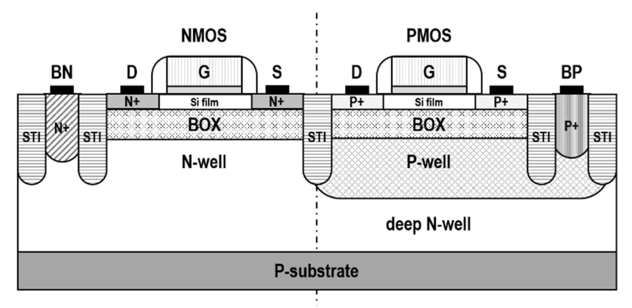
2. The 28 nm UTBB FD-SOI CMOS Technology
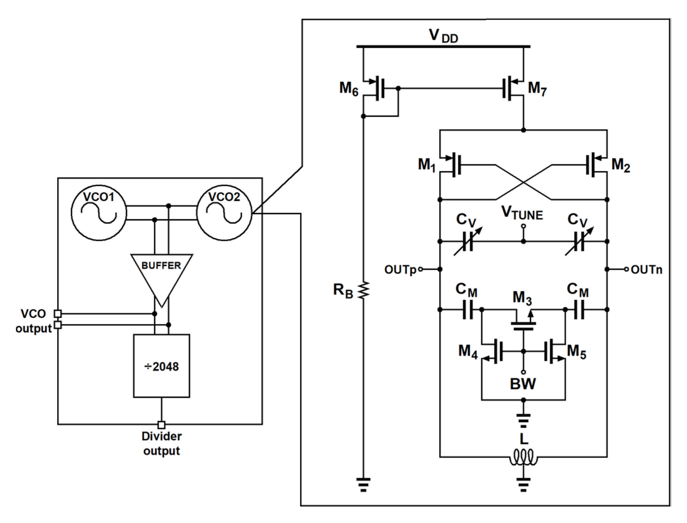
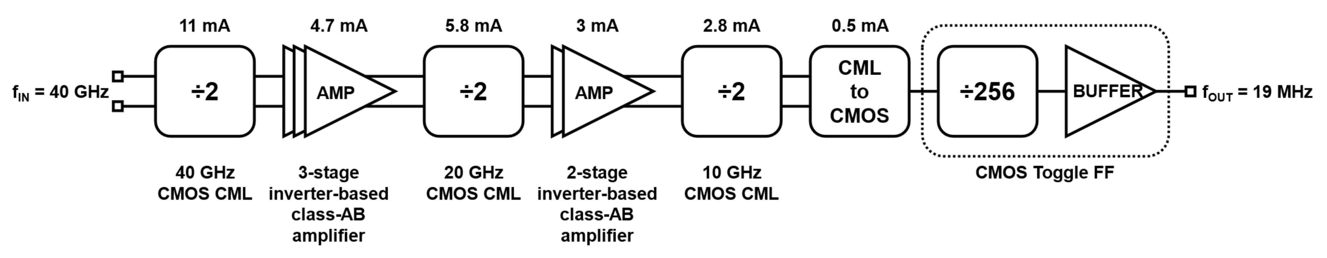
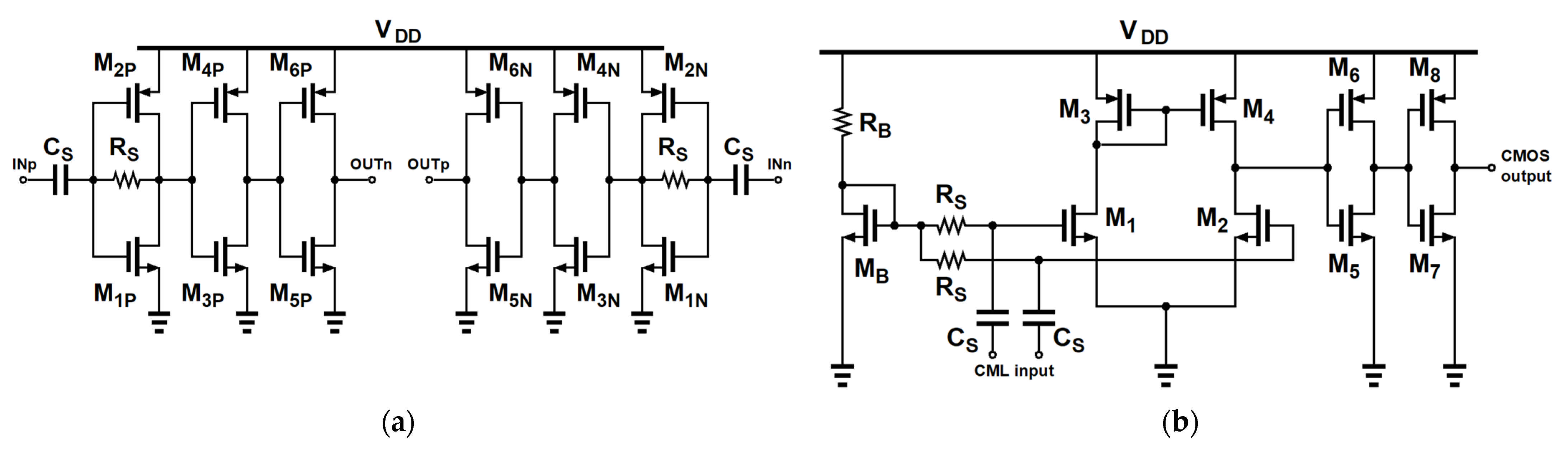
The 28 nm UTBB FD-SOI CMOS technology is one of the most promising technologies for developing high-speed, low-power analog and digital circuits, as well as radio frequency (RF) and mm-wave circuits. The technology adopted features high-k metal gate transistors fabricated on ultrathin silicon film (7 nm) sited above a thin (25 nm) buried oxide (BOX) layer, as shown in Figure 1. Owing to the ultrathin silicon film, the source and drain are isolated. The transistor channel is fully depleted, hence neither channel doping nor pocket implant are required. The thin BOX layer beneath the transistor channel acts as a second gate oxide and the N-well and P-well regions as additional gate terminals (i.e., back-gate terminals). These back-gates allow transistor threshold voltage (VT) to be properly adjusted through a wide range of body bias (BB) voltage [6,7,8,9].
The technology features two different transistor designs: conventional-well regular-VT (RVT) and flip-well low-VT (LVT). RVT transistors can adopt a reverse body-biasing (RBB) technique to increase threshold voltage, thus reducing leakage current. In contrast, LVT transistors can use a forward body-biasing (FBB) technique to reduce threshold voltage, thus increasing switching performance at the cost of a higher leakage current.
As previously demonstrated in [10,11,12,13], body-biasing techniques have been profitably used for compensating process, voltage, and temperature (PVT) variations, and for tuning circuit performance. Two gate oxide options are available for both RVT and LVT configuration. A thin gate oxide (1.3 nm) transistor has a nominal gate length and supply voltage of 28 nm and 1 V, respectively. A thick gate oxide (3.4 nm) transistor has a nominal gate length and supply voltage of 90 nm/130 nm and 1.5 V/1.8 V, respectively. The technology process also provides an accumulation MOS varactor (A-MOS) [14], and metal-oxide–metal (MoM) and metal-insulator–metal (MiM) capacitors with 6 and 16 fF/µm2, respectively. The technology process has a low-k BEOL with eight or ten copper layers along with a top aluminum (Alucap) layer.

3. Circuit Design

The schematic of the implemented VCOs is shown in Figure 2; two cores, that differ for tank inductance value, are integrated for compensating process and temperature variations. Each VCO has two continuous frequency tuning bands selectable by a single control bit (i.e., BW in Figure 2). Their core circuit is based on a differential cross-coupled topology using PMOS transistors and LC resonant tank. The use of cross-coupled PMOS transistors has two main advantages. First, VCO phase noise can be minimized because PMOS flicker noise is lower than that of an n-type metal-oxide–semiconductor (NMOS) transistor. Second, the accumulation MOS varactor gate is biased to ground through the inductor central tap; in this way, for positive tuning voltages, the A-MOS varactor works in depletion region where it features a higher quality factor. Moreover, no R-C network is used for varactor bias, further reducing VCO phase noise contributions, and maximizing capacitance tuning ratio. Transistors M1 and M2 are thin gate oxide LVT PMOS with gate width and length of 40 µm and 36 nm, respectively. The gate width is designed as a tradeoff between phase noise and frequency tuning range, meanwhile the gate length is designed to minimize phase noise. The back-gate of M1 and M2 are connected to ground (i.e., natural BB) to avoid any noise contribution coming from bias circuitry. Indeed, in the case of integrated circuit (IC) industrialization, a charge-pump circuit could be required for generating a negative bias voltage for applying FBB to an LVT PMOS transistor.
Thick gate oxide LVT transistors are used for current mirror (M6, M7). The gate width and length are 1260 µm and 3 µm, respectively. They are chosen for minimizing current mirror noise contribution and channel length modulation effect.
The resonant LC-tank consists of a single-turn inductor (L) with a central tap, accumulation MOS varactor (i.e., CV), and switched-capacitor bank (i.e., CM).
The tank inductor was fabricated using a two-layer structure (i.e., a top thick copper layer + Alucap). A patterned ground shield (PGS), made with the first thin copper layer, was used to guarantee a proper ground model in the simulation. An optimized inductor width of 11 um was chosen for obtaining the best tradeoff between quality factor (QL) and self-resonance frequency (SRF). Electromagnetic (EM) field solver (i.e., Keysight ADS Momentum) has been widely used to extract S-parameters of inductor and interconnections between the inductor itself and all the other VCO elements (i.e., cross-coupled active pairs, varactor, switched-capacitor bank, and ground plane). A 3D view of the inductor together with simulated inductance values and quality factors are shown in Figure 3a,b, respectively.
A thick gate oxide accumulation MOS varactor was used for realizing the continuous oscillation frequency control. According to technology reliability constraints, a maximum positive voltage of 1.8 V can be applied to VTUNE terminal. Finger width and gate length were set at 1 µm and 80 nm, respectively. They were chosen for acquiring the best tradeoff between varactor quality factor and capacitance tuning ratio. Indeed, the quality factor decreases when the capacitance tuning ratio is increased. At mm-wave frequencies, the quality factor of an LC resonator is typically limited by the varactor [15]. Unfortunately, there is a compromise between the maximum achievable continuous frequency tuning and phase noise. The VCO’s bands are selectable using a switched-capacitor bank, realized by using a shielded RF MoM capacitor. Its layout structure and model were developed for operating at very high frequencies. Each CM capacitor consists of four elementary cells of 10 fF. The π-switch structure consists of three thin gate oxide LVT NMOS (i.e., M3, M4, and M5) devices. The M3 device acts as a switch and the other two devices (M4 and M5) are used to bias the source and drain terminals of M3. The transistor sizes were optimized for achieving the best RON-COFF design tradeoff, thus limiting the impact on resonator quality factor and therefore on phase noise, while minimizing the effect on tuning range. The output buffer is a common-source amplifier with a resonant load, and is in common with both VCOs. The nominal supply voltage of VCOs and output buffer is 1.8 V. Because M1 and M2 are thin gate oxide LVT PMOS devices, the bias voltage of the source terminals is lower than 1 V. Moreover, the current consumption of VCO and its output buffer are 10 mA and 5 mA, respectively.
The high-frequency divider chain, whose block diagram is reported in Figure 4, consists of three static CMOS CML Master-Slave D-type Flip-Flop stages followed by a CML to CMOS converter and a divider-by-256 stage realized by using standard CMOS Toggle Flip-Flops. Three-stage and two-stage class-AB inverter-based amplifiers were added between high-frequency dividers to guarantee proper amplitude swing to drive the next divider stage in all PVT conditions. The nominal supply voltage was 1 V. The current consumption of each divider chain element is also specified in Figure 4.
The simplified schematic of the 40, 20, and 10 GHz divider is sketched in Figure 5. The three-stage inverter-based class-AB amplifier and CML to CMOS converter are depicted in Figure 6a,b, respectively. Thin gate oxide LVT NMOS transistors were used for divider stage design. Due to a low supply voltage, in high-frequency divider stages and in the CML to CMOS converter, a traditional tail current source was not used and the bias current was set through the diode-connected transistor MB; this allowed for saving voltage headroom and transistor work in the high-speed region. The signal is injected to divider input through the high-pass passive network: RS, CS. Transistor size, bias current, and load resistors were scaled according to the operative frequency (i.e., 40, 20, and 10 GHz).
The back-gates of NMOS transistors were biased at VDD for exploiting the maximum switching performance. The complete divider chain has a power consumption of 27.8 mW at 1 V supply voltage.

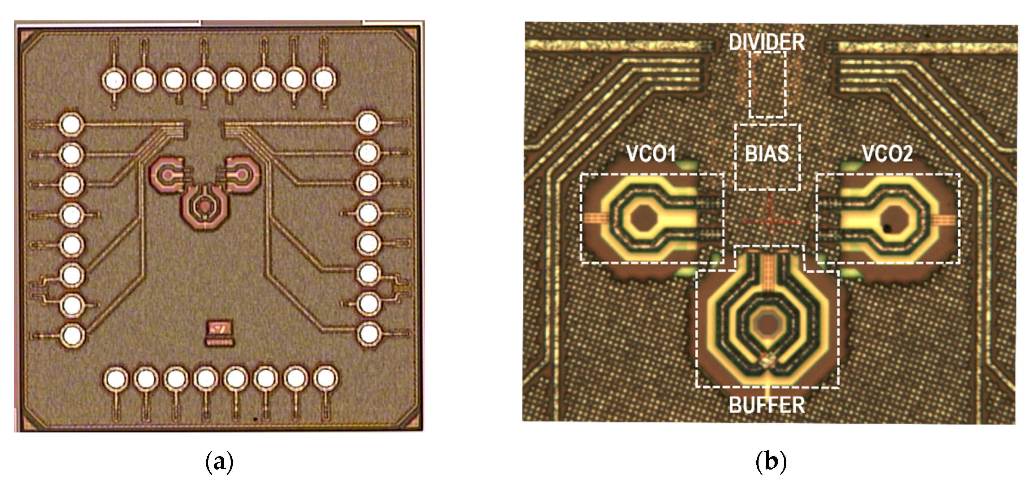
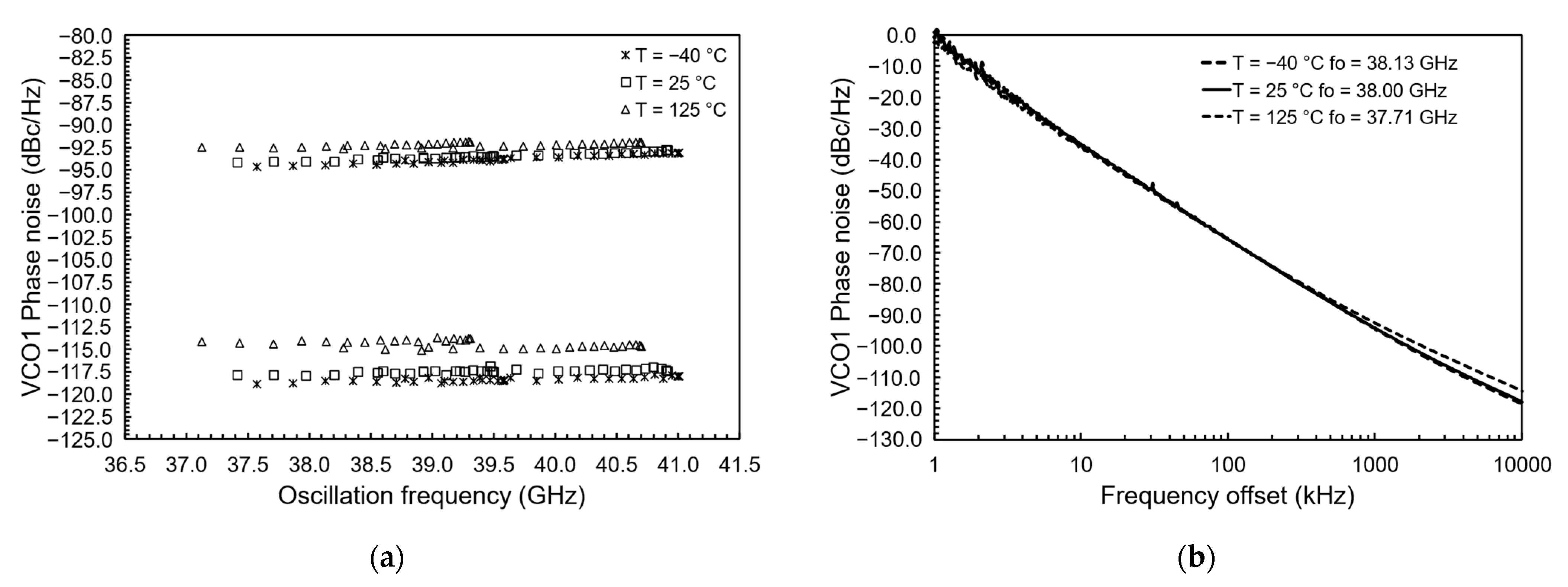
4. Experimental Results

The proposed circuits were fabricated in a STMicroelectronics 28 nm UTBB FD-SOI CMOS process with the eight metal layers BEOL option. Die microphotographs are reported in Figure 7. The die area is 2.2 mm2, and it is pad limited. The silicon area of the VCO, output buffer, and frequency divider chain are 0.027, 0.032, and 0.005 mm2, respectively.
Measurements were performed on-wafer and on testing printed circuit board (PCB) through a chip-on-board assembly of bare dice. In particular, VCO, TR, and PN were measured on-wafer from high-frequency VCO output using a wafer prober connected to a phase noise analyzer and VCO tester. In addition, the low frequency signal from divider chain output (i.e., 19 MHz) was measured on testing PCB using a signal source analyzer and an oscilloscope. VCO and divider chain were supplied at 1.8 and 1 V, respectively.
Figure 8a shows the VCO1 TR measured on three dice located on different wafer positions at room temperature. The tuning voltage (i.e., VTUNE) was swept from 0 to 1.8 V. VCO1 shows a measured TR of 3.5 GHz. The maximum frequency difference between the measured and the simulated curves is 1.6%. The VCO1 TR and PN were also measured at three different temperatures (i.e., −40, 25, and 125 °C). The tuning range curves vs. temperature are shown in Figure 8b. The average value of frequency thermal drift, mainly due to the temperature behavior of the accumulation MOS varactor, is about −3 MHz/°C.
The single-sideband PN vs. oscillation frequency measured at 1 and 10 MHz frequency offset is reported in Figure 9a. The measured PN is between −93 and −94.3 dBc/Hz at 1 MHz offset, and it is between −116.9 and −118 dBc/Hz at 10 MHz offset at T = 25 °C. PN improves by 1 dB at T = −40 °C and it degrades by 2 dB at T = 125 °C. The PN performance is almost constant throughout the whole VCO1 TR. For completeness, Figure 9b reports VCO1 PN performance at three different temperatures vs. frequency offset; in this case the oscillation frequency was set at 38 GHz at room temperature. VCO2 TR characteristics of three different dice at room temperature, TR at three different temperatures, and PN performance were measured as well. VCO2 oscillates at lower frequency and its measured TR is about 3.5 GHz. The average value of frequency band overlap for VCO2 upper band (i.e., VCO2 BW = 0) and VCO1 lower band (i.e., VCO1 BW = 1) is about 650 MHz. The measured current consumption of VCO and its output buffer is about 15.4 mA at T = 25 °C at 1.8 V supply voltage.
The frequency divider chain functionality was proved to exploit the whole VCOs TR (i.e., from f0MIN = 36.7 GHz to f0MAX = 41 GHz). It was also tested at three temperatures (i.e., −40, 25, and 125 °C) for worst case conditions with a minimum supply voltage of 0.9 V (i.e., 10% lower with respect to nominal value). The measured current consumption of the frequency divider chain is about 26.9 mA at T = 25 °C and 1 V supply voltage.
The performance of the proposed VCO is compared in Table 1 with state-of-the art VCOs fabricated using similar CMOS processes. The well-known figure of merit (FOM) was used for benchmarking VCOs.
Assuming a theoretical profile of out-of-band PLL PN decreasing by 20 dB/dec, the equation in [5] predicts a flat equivalent noise figure due to DPN with a reduction of the receiver sensitivity. As consequence, the oscillator PN performance for offset in the range of 5 to 10 MHz is a key parameter for applying S/N optimization. The proposed VCO shows better PN and FOM at 10 MHz offset with respect to [20], which targets the same oscillation frequency and application. The best PN performance is presented in [16], but the oscillator works at lower frequency and its power consumption is much higher.

5. Conclusions

In this paper, the design and measurements of 40-GHz VCO for a radar automotive sensor are reported and discussed. The circuit also includes a high-frequency divider chain. Owing to an accurate circuit, EM co-design strategy, and layout optimization, state-of-the art performance is achieved in an advanced 28 nm ultrathin body and box fully depleted silicon-on-insulator CMOS technology, which enables a low-cost SoC approach for the radar automotive system.

Author Contributions

Conceptualization, G.M. and A.S.; methodology, G.M.; validation, G.M.; formal analysis, G.M. and S.S.; investigation, G.M. and G.C.; resources, M.G.; data curation, G.M.; writing—original draft preparation, G.M.; writing—review and editing, S.S. and A.S.; visualization, G.M.; supervision, M.G.; project administration, A.S. and M.G. All authors have read and agreed to the published version of the manuscript.

Funding

This research received no external founding.

Acknowledgments

The authors would like to thank P. Lizzio and F. Alonso of STMicroelectronics, Catania, Italy, for the layout design and validation support, respectively.

Conflicts of Interest

The authors declare no conflict of interest.

References

  1. Guermandi, D.; Shi, Q.; Dewilde, A.; Derudder, V.; Ahmad, U.; Spagnolo, A.; Ocket, I.; Bourdoux, A.; Wambacq, P.; Craninckx, J.; et al. A 79-GHz 2 × 2 MIMO PMCW Radar SoC in 28-nm CMOS. IEEE J. Solid-State Circuits 2017, 52, 2613–2626. [Google Scholar] [CrossRef]
  2. Ma, T.; Deng, W.; Chen, Z.; Wu, J.; Zheng, W.; Wang, S.; Qi, N.; Liu, Y.; Chi, B. A CMOS 76–81-GHz 2-TX 3-RX FMCW Radar Transceiver Based on Mixed-Mode PLL Chirp Generator. IEEE J. Solid-State Circuits 2020, 55, 233–248. [Google Scholar] [CrossRef]
  3. Giannini, V.; Goldenberg, M.; Eshraghi, A.; Maligeorgos, J.; Lim, L.; Lobo, R.; Welland, D.; Chow, C.; Dornbusch, A.; Dupuis, T.; et al. A 192-Virtual-Receiver 77/79 GHz GMSK Code-Domain MIMO Radar System-on-Chip. In Proceedings of the IEEE International Solid-State Circuits Conference Digest of Technical Papers, San Francisco, CA, USA, 17–21 February 2019; pp. 164–166. [Google Scholar]
  4. Patole, S.M.; Torlak, M.; Wang, D.; Ali, M. Automotive radars: A review of signal processing techniques. IEEE Signal. Process. Mag. 2017, 34, 22–35. [Google Scholar] [CrossRef]
  5. Melzer, A.; Onic, A.; Starzer, F.; Huemer, M. Short-Range Leakage Cancelation in FMCW Radar Transceivers Using an Artificial On-Chip Target. IEEE J. Sel. Top. Signal. Process. 2015, 9, 1650–1660. [Google Scholar] [CrossRef]
  6. Pelloux-Prayer, B.; Blagojević, M.; Haendler, S.; Valentian, A.; Amara, A.; Flatresse, P. Performance analysis of multi-VT design solutions in 28 nm UTBB FD-SOI technology. In Proceedings of the IEEE International SOI-3D-Subthreshold Microelectronics Technology Unified Conference (S3S), Monteray, CA, USA, 7–10 October 2013; pp. 1–2. [Google Scholar]
  7. Shopov, S.; Voinigescu, S.P. Characterization of the High Frequency Performance of 28-nm UTBB FDSOI MOSFETs as a Function of Backgate Bias. In Proceedings of the IEEE Compound Semiconductor Integrated Circuit Symposium (CSICS), La Jolla, CA, USA, 19–22 October 2014; pp. 1–4. [Google Scholar]
  8. El Ghouli, S.; Scheer, P.; Minondo, M.; Juge, A.; Poiroux, T.; Sallese, J.M.; Lallement, C. Analog and RF modeling of FDSOI UTBB MOSFET using Leti-UTSOI model. In Proceedings of the MIXDES—23rd International Conference Mixed Design of Integrated Circuits and Systems, Lodz, Poland, 23–25 June 2016; pp. 41–46. [Google Scholar]
  9. Makovejev, S.; Kazemi Esfeh, B.; Barral, V.; Planes, N.; Haond, M.; Flandre, D.; Raskin, J.-P.; Kilchytska, V. Wide frequency band assessment of 28 nm FDSOI technology platform for analogue and RF applications. In Proceedings of the 15th International Conference on Ultimate Integration on Silicon (ULIS), Stockholm, Sweden, 7–9 April 2014; pp. 53–56. [Google Scholar]
  10. Lechevallier, J.; Struiksma, R.; Sherry, H.; Cathelin, A.; Klumperink, E.; Nauta, B. A forward-body-bias tuned 450 MHz Gm-C 3rd-order low-pass filter in 28 nm UTBB FD-SOI with >1 dBVp IIP3 over a 0.7-to-1 V supply. In Proceedings of the IEEE International Solid-State Circuits Conference Digest of Technical Papers, San Francisco, CA, USA, 23–26 February 2015; pp. 1–3. [Google Scholar]
  11. Sourikopoulos, I.; Frappé, A.; Cathelin, A.; Clavier, L.; Kaiser, A. A digital delay line with coarse/fine tuning through gate/body biasing in 28 nm FDSOI. In Proceedings of the IEEE 42nd European Solid-State Circuits Conference, Lausanne, Switzerland, 12–15 September 2016; pp. 145–148. [Google Scholar]
  12. De Streel, G.; Stas, F.; Gurné, T.; Durant, F.; Frenkel, C.; Cathelin, A.; Bol, D. SleepTalker: A ULV 802.15.4a IR-UWB Transmitter SoC in 28-nm FDSOI Achieving 14 pJ/b at 27 Mb/s With Channel Selection Based on Adaptive FBB and Digitally Programmable Pulse Shaping. IEEE J. Solid-State Circuits 2017, 52, 1163–1177. [Google Scholar] [CrossRef]
  13. Finocchiaro, A.; Papotto, G.; Ragonese, E.; Palmisano, G. A 28-nm FD-SOI CMOS Variable-Gain Amplifier With Body-Bias-Based DC-Offset Cancellation for Automotive Radars. IEEE Trans. Circuits Syst. II Express Briefs 2019, 66, 1693–1697. [Google Scholar] [CrossRef]
  14. Quemerais, T.; Gloria, D.; Golanski, D.; Bouvot, S. High-Q MOS Varactors for Millimeter-Wave Applications in CMOS 28-nm FDSOI. IEEE Electron. Dev. Lett. 2015, 36, 87–89. [Google Scholar] [CrossRef]
  15. Cao, C.; O, K.K. Millimeter-wave voltage-controlled oscillators in 0.13-/spl mu/m CMOS technology. IEEE J. Solid-State Circuits 2006, 41, 1297–1304. [Google Scholar] [CrossRef]
  16. Reiter, D.; Li, H.; Knapp, H.; Kammere, J.; Majied, S.; Sene, B.; Pohl, N. A Low Phase Noise, Wide Tuning Range 20GHz Magnetic-Coupled Hartley-VCO in a 28 nm CMOS Technology. In Proceedings of the IEEE Radio and Wireless Symposium (RWS), Orlando, FL, USA, 20–23 January 2019; pp. 1–3. [Google Scholar]
  17. Hu, Y.; Siriburanon, T.; Staszewski, R.B. A Low-Flicker-Noise 30-GHz Class-F23 Oscillator in 28-nm CMOS Using Implicit Resonance and Explicit Common-Mode Return Path. IEEE J. Solid-State Circuits 2018, 53, 1977–1987. [Google Scholar] [CrossRef] [Green Version]
  18. Vigilante, M.; Reynaert, P. A coupled-RTWO-based subharmonic receiver front-end for 5G E-Band backhaul links in 28 nm bulk CMOS. In Proceedings of the IEEE International Solid-State Circuits Conference Digest of Technical Papers, San Francisco, CA, USA, 11–15 February 2018; pp. 412–414. [Google Scholar]
  19. Zhang, C.; Otto, M. A wide range 60 GHz VCO using back-gate controlled varactor in 22 nm FDSOI technology. In Proceedings of the IEEE International SOI-3D-Subthreshold Microelectronics Technology Unified Conference (S3S), San Francisco, CA, USA, 16–19 October 2017; pp. 1–3. [Google Scholar]
  20. Bai, J.; Lee, J.; Zhang, J.; Rohani, N. A 28-nm CMOS 40-GHz high-resolution digitally controlled oscillator for automotive radar applications. In Proceedings of the IEEE 17th Topical Meeting on Silicon Monolithic Integrated Circuits in RF Systems (SiRF), Phoenix, AZ, USA, 15–18 January 2017; pp. 91–93. [Google Scholar]
  21. Mammei, E.; Monaco, E.; Mazzanti, A.; Svelto, F. A 33.6-to-46.2 GHz 32 nm CMOS VCO with 177.5 dBc/Hz minimum noise FOM using inductor splitting for tuning extension. In Proceedings of the IEEE International Solid-State Circuits Conference Digest of Technical Papers, San Francisco, CA, USA, 17–21 February 2013; pp. 350–351. [Google Scholar]
Figure 1. Simplified cross-section of a flipped-well n-type metal-oxide–semiconductor (NMOS) and with p-type metal-oxide–semiconductor (PMOS) transistors [7].
Electronics 10 02114 g001
Figure 2. Simplified block diagram and voltage-controlled oscillator (VCO) schematic.
Electronics 10 02114 g002
Figure 3. Single-turn octagonal inductor: (a) 3D view with metal stack-up and (b) simulated inductance and quality factor.
Electronics 10 02114 g003
Figure 4. Simplified block diagram of the high-frequency divider chain.
Electronics 10 02114 g004
Figure 5. Schematic of the divider stage based on static complementary metal-oxide–semiconductor (CMOS) current-mode logic (CML) Master-Slave D-type Flip-Flop.
Electronics 10 02114 g005
Figure 6. (a) Simplified schematic of 3-stage inverted-based class-AB amplifier; (b) simplified schematic of CML to CMOS converter.
Electronics 10 02114 g006
Figure 7. (a) Die microphotograph; (b) VCO core detail.
Electronics 10 02114 g007
Figure 8. Measured VCO tuning range: (a) simulations and measurements over three dice at T = 25 °C; (b) measurements at three different temperatures.
Electronics 10 02114 g008
Figure 9. Measured VCOs single-sideband phase noise: (a) at 1 and 10 MHz frequency offset at three different temperatures; (b) vs. frequency offset at three different temperatures.
Electronics 10 02114 g009
Table 1. VCO performance summary and state-of-the art comparison.
UnitThis WorkRWS 2019
[16]
JSSC 2018
[17]
ISSCC 2018
[18]
SOI-3D 2017
[19]
SiRF 2017
[20]
ISSCC 2013
[21]
Technology 28 nm FD-SOI28 nm bulk28 nm bulk28 nm bulk22 nm FD-SOI28 nm bulk32 nm bulk
FrequencyGHz4018.729.318604040
Tuning rangeGHz3.52.23.93.7213.612.6
PN at 1 MHzdBc/Hz−94.3−113.8−106-−84.3−99.5 (2)-
PN at 10 MHzdBc/Hz−118−133-−131.2 (3)−108.6−115 (3)−115.2/−118
Supply voltageV1.81.811.30.711
Pwr consumptionmW18901282 (3)7.510.59.8
FOM (1)dBc/Hz−177.5−179.7−184−176.7−175.8−176.7−177.3/−180
(1) FOM = PN f 20 log f 0 f + 10 log P DC mW ; (2) measured at 39.3 GHz; (3) value extracted from measurement plots.
Publisher’s Note: MDPI stays neutral with regard to jurisdictional claims in published maps and institutional affiliations.

