Article

A Pipelined Noise-Shaping SAR ADC Using Ring Amplifier

Department of Electrical and Electronic Engineering, Konkuk University, Seoul 05029, Korea
*
Author to whom correspondence should be addressed.
Electronics 2021, 10(16), 1968; https://doi.org/10.3390/electronics10161968
Submission received: 12 July 2021 / Revised: 12 August 2021 / Accepted: 13 August 2021 / Published: 15 August 2021
(This article belongs to the Special Issue Advances on Analog-to-Digital and Digital-to-Analog Converters)

Abstract

:
In this study, a pipelined noise-shaping successive-approximation register analog-to-digital converter (PLNS-SAR ADC) structure was proposed to achieve high resolution and to be free from comparator design requirements. The inter-stage amplifier and integrator of the PLNS-SAR ADC were implemented through a ring amplifier with high gain and speed. The ring amplifier was designed to improve power efficiency and be tolerant to process–voltage–temperature (PVT) variation, and uses a single loop common-mode feedback (CMFB) circuit. By processing residual signals with a single ring amplifier, power efficiency can be maximized, and a low-power system with 30% lower power consumption than that of a conventional PLNS-SAR ADC is implemented. With a high-gain ring amplifier, noise leakage is greatly suppressed, and a structure can be implemented that is tolerant of mismatches between the analog loop and digital correction filters. The measured signal to noise distortion ratio (SNDR) is 70 dB for a 5.15 MHz bandwidth (BW) at a 72 MS/s sampling rate (Fs) with an oversampling ratio (OSR) of 7, and the power consumption is 2.4 mW. The FoM S , SNDR   (= SNDR + 10 log 10 BW/Power) is 163.5 dB. The proposed structure in this study can achieve high resolution and wide BW with good power efficiency, without a filter calibration process, through the use of a ring amplifier in the PLNS-SAR ADC.

1. Introduction

Recently, the demand for a high-performance analog-to-digital converter (ADC) has increased due to digital systems that need to process large amounts of data at high speeds. In addition, there have been continuing attempts to develop ADCs that can minimize power consumption while possessing a structure optimized for complementary metal-oxide-semiconductor (CMOS) process scaling [1,2]. Various ADC structures have been developed to meet these requirements, most of which are based on successive-approximation register ADCs (SAR ADCs) with good power efficiency [3,4]. However, SAR ADCs have a limit for increasing resolution, regardless of power efficiency. This is because the conventional method endeavors to improve resolution by increasing the SAR quantizer bit number. In-band noise can decrease by 6 dB with each increase in quantization bit, but comparator noise also has to be attenuated, which not only greatly decreases the speed of the comparator, but also increases power consumption. To overcome the limitations set by the comparator, an SAR ADC can be combined with a pipeline structure [5,6]. Figure 1 displays a block diagram of a pipeline-SAR ADC, with two structures combined. It consists of a 1st stage for quantizing the most significant bits (MSBs), 2nd stage for quantizing the least significant bits (LSBs), and inter-stage amplifier for amplifying the residual voltage of the 1st stage. In the 1st stage, digital output 1 ( D OUT 1 ) is obtained through SAR conversion after sampling the input voltage (VIN). Subsequently, the residual voltage generated in the 1st stage is amplified by the inter-stage gain (G) and transferred to the 2nd stage input. Digital output 2 ( D OUT 2 ) is obtained through the 2nd stage SAR conversion. The final output ( D OUT ) can be obtained after the output of each stage is processed with a digital correction filter. D OUT ideally shows only V IN , 2nd stage quantization noise ( Q 2 ), and 2nd stage comparator noise ( N CMP 2 ). The 1st stage quantization noise ( Q 1 ) and comparator noise ( N CMP 1 ) can be removed through a digital correction filter, and Q 2 and N CMP 2 can be attenuated by 1/G through the pipeline structure, so high resolution can be obtained. Due to the suppression of Q 2 , the comparator accuracy requirement is lowered, and the speed bottleneck problem of SAR ADCs can be solved because MSBs and LSBs are simultaneously converted through the pipeline operation. However, in the pipeline structure, if the G is not accurate, noise leakage occurs due to filter mismatch, and its performance is greatly reduced. To prevent mismatch of the G and digital correction filter due to finite gain and nonlinearity of the amplifier, the high gain operational amplifier (op-amp) structure is widely used, either gain-boosted, using a cascode, or other methods [7]. However, because of static current, the power consumption of an op-amp is very large, and the ADC speed is slow due to the long amplification time. Furthermore, the difficulty of designing a high gain op-amp is increased with the scaling of the CMOS process. Another alternative, the dynamic amplifier, can be used to mitigate the speed and power consumption problems of op-amps [8]. Because static operation is not performed, power consumption is efficient, and fast amplification is possible through a simple structure. However, additional calibration blocks are needed because of its open-loop operation, so design complexity is increased. The ring amplifier is advantageous for use in ADCs with a pipeline structure to achieve high resolution because it exhibits fast and stable operation and very low power consumption, unlike the aforementioned amplifiers [9].
A ring amplifier is a structure based on a ring oscillator composed of three inverters. Three single-stage inverters can achieve high gain without complex gain enhancement techniques or calibration. Thus, accurate G can be implemented and has a simple structure, which enables easy scalability. In addition, the signal can be rapidly amplified through slew-based charging rather than the RC-based charging used in conventional op-amps, and power consumption is very low. The values of the parameters listed in Table 1 confirm that, using a ring amplifier, a pipeline structure can be advantageous in terms of power and speed without additional circuits [10,11,12,13]. However, even if a ring amplifier is used, if a pipeline-SAR ADC tries to implement even higher resolution, each stage requires further fine quantization, and the comparator design can be an issue. A noise-shaping technique can be applied to implement ADCs with a pipeline structure completely free from comparator requirements [14,15]. When a loop filter is applied to each pipeline stage and high-order noise-shaping is implemented, overall, high resolution can be achieved without using fine quantization. Therefore, this paper proposes a pipelined noise-shaping SAR ADC (PLNS-SAR ADC) that can improve speed and power efficiency using a ring amplifier, achieving high resolution by applying noise-shaping at each pipeline stage. This paper is organized as follows: Section 2 displays the architecture of this work, Section 3 describes circuit implementation, Section 4 presents the measurement results, and Section 5 presents the conclusion.

2. Architecture

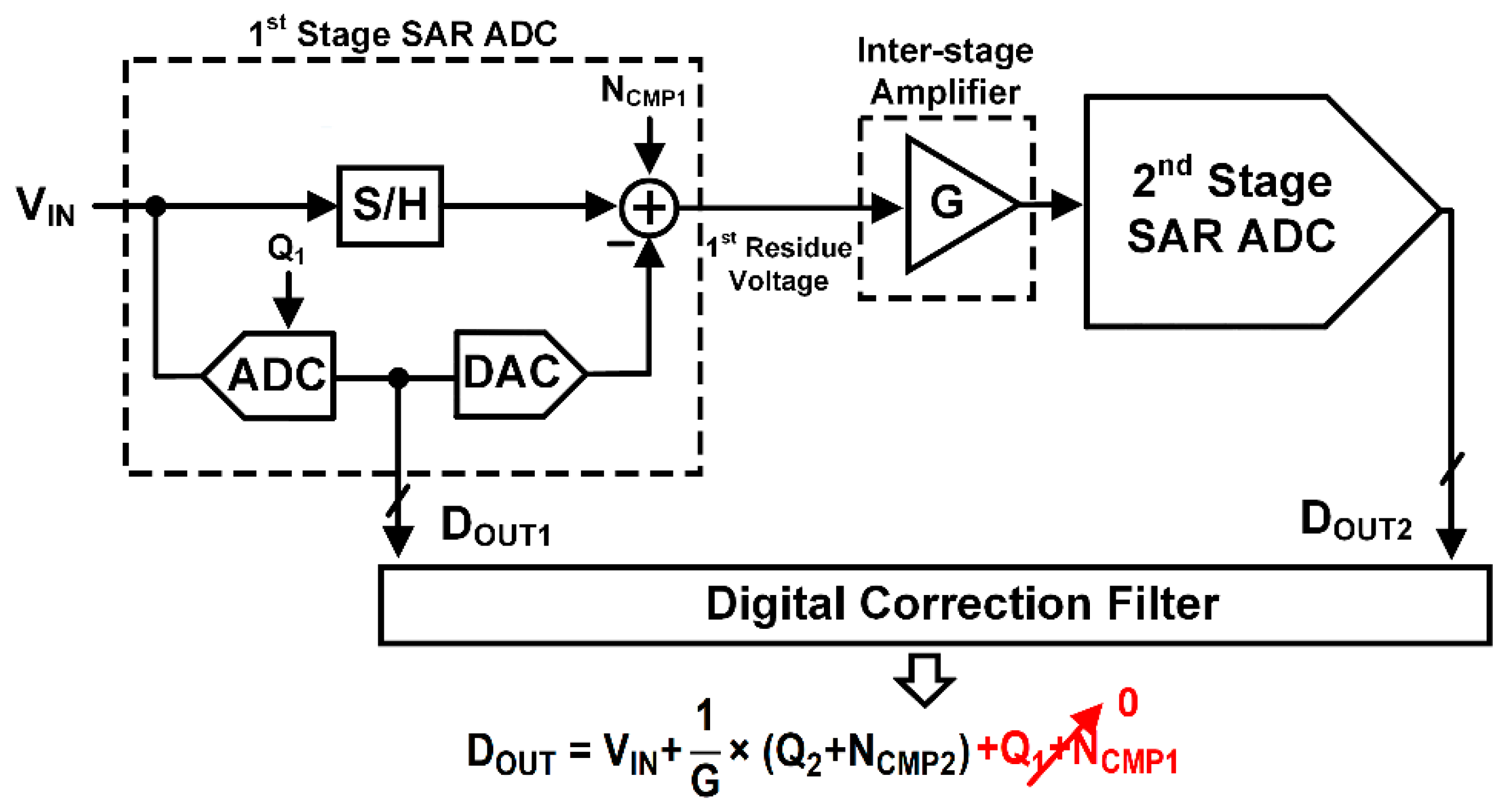
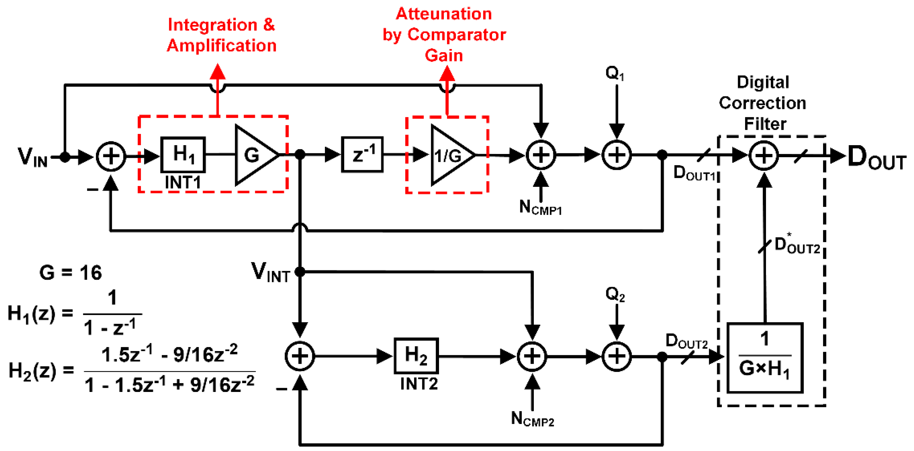
2.1. Pipelined Noise-Shaping SAR ADC
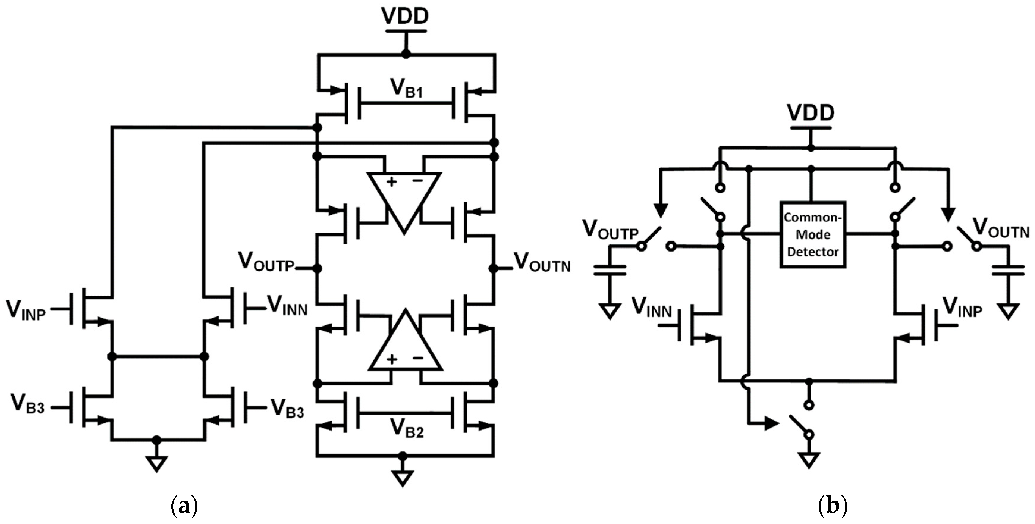
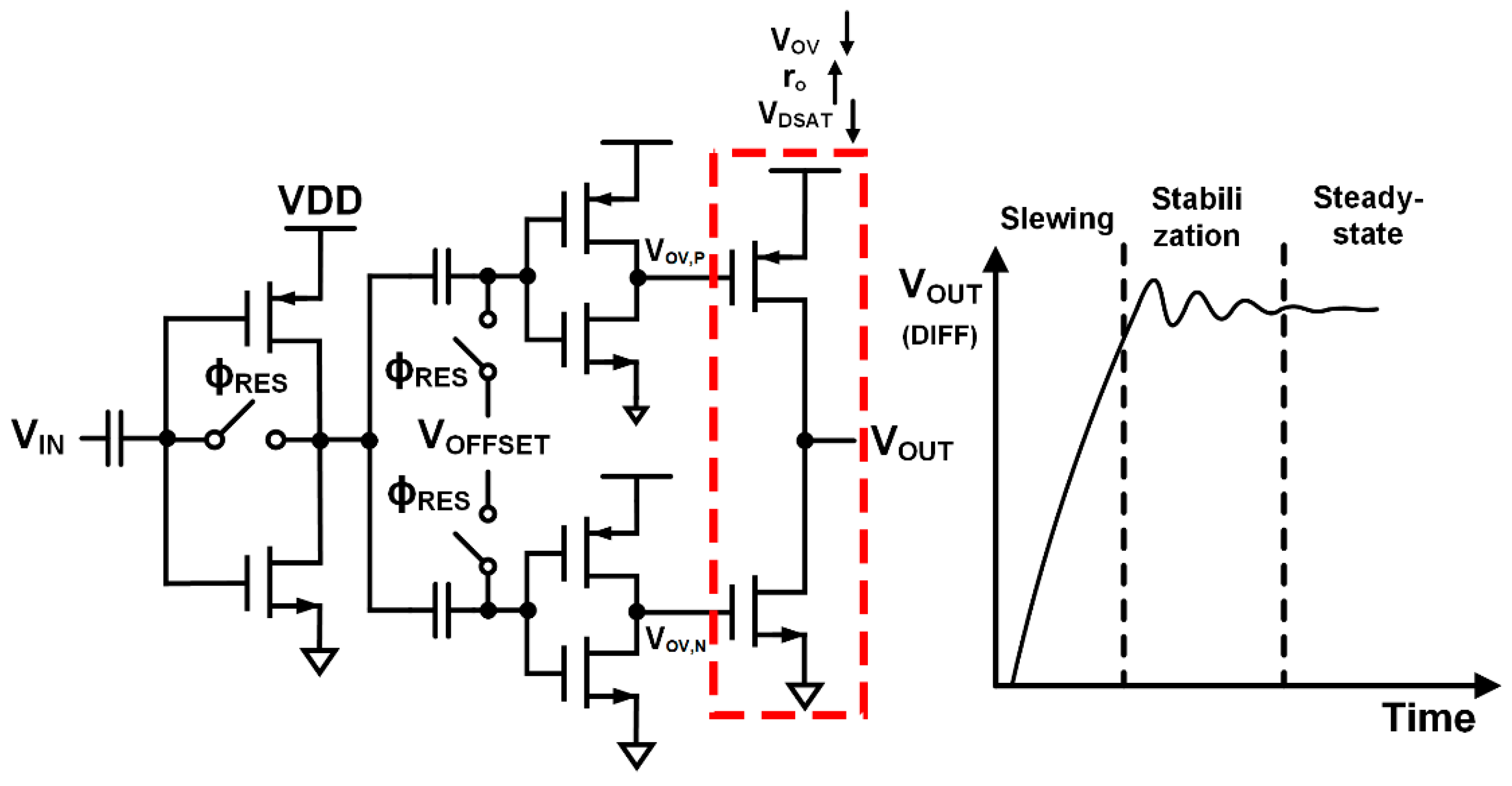
Figure 2 displays the PLNS-SAR ADC block diagram [16,17]. A loop filter is applied to a coarse quantizer to achieve high resolution while maintaining the advantage of a pipelined structure. Integrators (INT1 and INT2) are used as the loop filter for each stage, and there is an inter-stage amplifier for amplifying the integrated 1st stage residual voltage. The 1st stage loop filter is an active type, for the implementation of a sharp noise transfer function (NTF). To alleviate the power consumption problem, which is a disadvantage of the active type, integration and amplification are performed simultaneously by a single amplifier to prevent the additional use of an amplifier [16,17,18]. To maintain the original transfer function of the loop filter, the amplified signal is attenuated again by a multi-input comparator gain. The 2nd loop filter uses a passive type to minimize power consumption while allowing the overall NTF to have a high order [19,20].
The final digital output ( D OUT ) can be derived as follows. The digital output of the 1st stage ( D OUT 1 ) is expressed as:
D OUT 1 = V IN   + ( 1     z 1 ) · ( Q 1   + N CMP 1 )
The residue voltage of the 1st stage, which is generated by applying D OUT 1 to a capacitive digital-to-analog converter (CDAC) in the SAR loop and by subtracting it from VIN, is transferred to the input of the 2nd stage ( V INT ) after integration and amplification. V INT and the digital output of the 2nd stage ( D OUT 2 ) are expressed as:
V INT   =   16 · ( Q 1   +   N CMP 1 )
D OUT 2   =   V INT   +   ( 1 0 . 75 z 1 ) 2 · ( Q 2   +   N CMP 2 )
Then, D OUT 2 is multiplied by ( 1   z 1 ) / 16   and added to D OUT 1 by the digital correction filter generating the final digital output D OUT , which is expressed as:
D OUT   =   D OUT 1   + 1 16 · ( 1     z 1 ) · D OUT 2   =   V IN   +   1 16 · ( 1   z 1 ) · ( 1     0 . 75 z   1 ) 2 · ( Q 2   +   N CMP 2 )
If the analog filter and digital correction filter are matched correctly, Q 1 and N CMP 1 are canceled, and Q 2 and N CMP 2 are not only shaped in the 3rd order, but also attenuated by 1/G to achieve high resolution.
As mentioned above, the structure can realize high resolution if the loop filter ( G   ×   H 1 ) and digital correction filter are matched. However, when the filter mismatch occurs because of the use of a non-ideal loop filter, the deleted noise components appear in noise-leakage form. When the PLNS-SAR structure uses conventional 1–2 multi-stage noise-shaping (MASH) [16,17,21], the noise-shaping applied to the 1st stage reduces the amount of leakage and alleviates the leakage effects. However, this structure still requires filter calibration. If the inter-stage amplifier is implemented using a high-gain amplifier in a closed-loop, a structure tolerable to filter mismatch can be implemented. Figure 3a,b displays histograms showing the signal-to-quantization ratio (SQNR) according to the open-loop gain of the amplifier with a 5% variation, and filter calibration is not performed. It can be seen that a high SQNR of ~75 dB or more can be obtained without additional filter calibration if a higher open-loop gain is used. Therefore, it is very important to use a high-gain amplifier to implement a tolerant structure for filter mismatch.

2.2. Ring Amplifier

An op-amp/operational trans-conductance amplifier (OTA) with a high open-loop gain is used in most pipelined structures because of its tolerance to filter mismatch. Among the various structures available, a gain-boosting, cascode-type op-amp is often used conventionally, as shown in Figure 4a [7,13,22,23]. However, it accounts for most of the ADC power consumption because of static current and is the biggest speed bottleneck in pipelined structures due to its long amplification time. Implementing large gain becomes more difficult because of the reduction of intrinsic gain and supply voltage due to CMOS technology scaling. Therefore, when a conventional structure is used in a low-scale CMOS process, it is difficult to obtain a DC gain of 50 dB or more despite the very large power consumption, so there is a problem that it is still vulnerable to filter mismatch. Additionally, the stack structure of op-amps/OTAs is not suitable for low supply voltage, because it can seriously affect linearity due to the limitation of the output swing range.
Another alternative is a dynamic amplifier, as shown in Figure 4b [11,24,25]. Dynamic amplifiers can operate quickly through a simple structure, have a large swing range, and have very good power efficiency without using static current. However, the gain is composed of complex nonlinear components. The output stage common-mode (CM) detector for determining amplification time is particularly vulnerable to process–voltage–temperature (PVT) variation, which has the biggest effect on linearity. Nonlinearity is a signal-dependent error, so it is not attenuated by filter calibration and degrades the overall resolution. Linearization techniques [26] using digital background calibration can significantly attenuate harmonics. However, as the target accuracy increases, the circuit design complexity increases exponentially. Therefore, a dynamic amplifier is more suitable for use in a pipelined structure with relatively low resolution.
To overcome the limitations of conventional op-amp and dynamic amplifier, a ring amplifier consisting of three inverters can be considered [9,10,14,27]. The triple inverter structure has advantages in various aspects such as gain, power efficiency, and swing. However, because it has the same structure as a ring oscillator, it cannot operate as an amplifier if stability is not guaranteed. By dynamically relocating the pole position of the ring oscillator, the stability can be increased and, as a result, the implementation of a ring amplifier is possible.
Figure 5 shows the structure and operation of a conventional ring amplifier. The 2nd stage is separated into two paths in the conventional three-stage inverter structure, and an offset voltage is applied between the input of each path for settling. In the slewing phase, the 1st and 2nd stages operate as rail-to-rail inverters to generate max gate overdrive voltage ( V OV ) for devices in the last inverter stage. This generates the maximum slew-current to charge/discharge the output stage load quickly. The slewing phase turns into a stabilization phase where the ring structure causes the signal to oscillate. The offset voltage reduces V OV during oscillation, and the last stage output current decreases, thereby reducing the oscillation amplitude. As the decrease continues, the amplifier approaches a steady state. In a steady state, the input voltage ( V IN ) becomes the virtual ground voltage, and the devices of the last-stage inverters go into the weak inversion region due to the offset voltage. Therefore, the output resistance ( r o ) of the output devices becomes very large, which dynamically shifts the output pole position of the amplifier. Eventually, the ring amplifier can be stabilized because the output pole, which was in an unstable position, moves to the low-frequency region and becomes a dominant pole. The output-stage device with class-AB behavior has a minimum V OV and V DSAT and a maximum r o in the steady state, so it shows rail-to-rail swing and can achieve a low quiescent current, high linearity, and high gain. Moreover, unlike a conventional op-amp, the power consumption can be dramatically reduced because it performs the slew-based charging through the dynamic operation like a digitally switched current source [27]. Generally, the performance of an op-amp follows the transconductance   ( g m ) / load relationship, and the power consumption is also proportional to that. However, a ring amplifier can have a maximum slew rate in the slewing state regardless of the load size and last-stage transistor size, so the power consumption by output load is free. A ring amplifier can minimize the performance constraints of the amplifier by the load while maximizing gain, speed, and power efficiency. Therefore, a ring amplifier is highly suitable for the inter-stage amplifier implementation, unlike a conventional op-amp and a dynamic amplifier. Finally, a ring amplifier can be applied to the proposed ADC structure by transforming the switch logic conventionally used for amplification so that it can perform both amplification and integration.

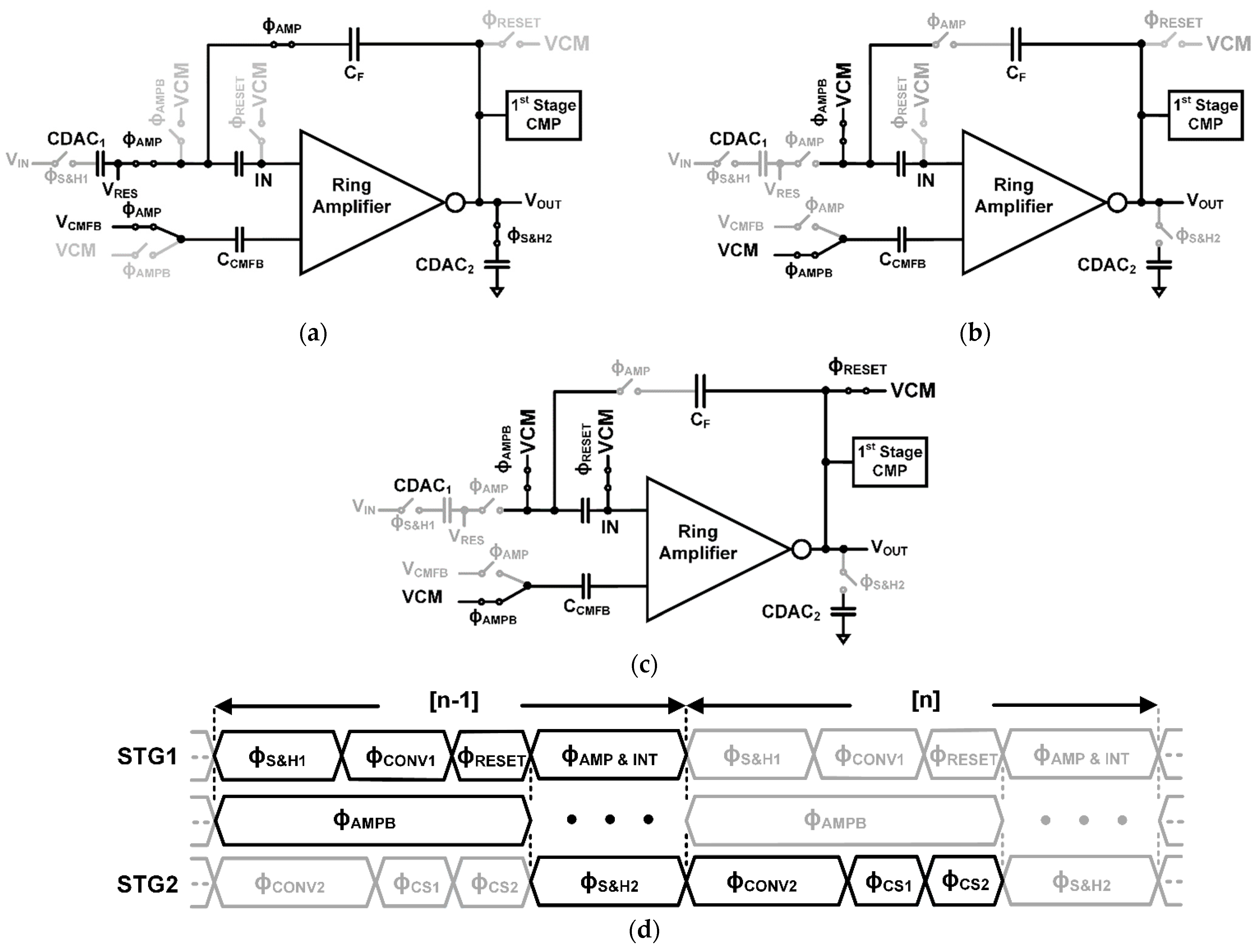
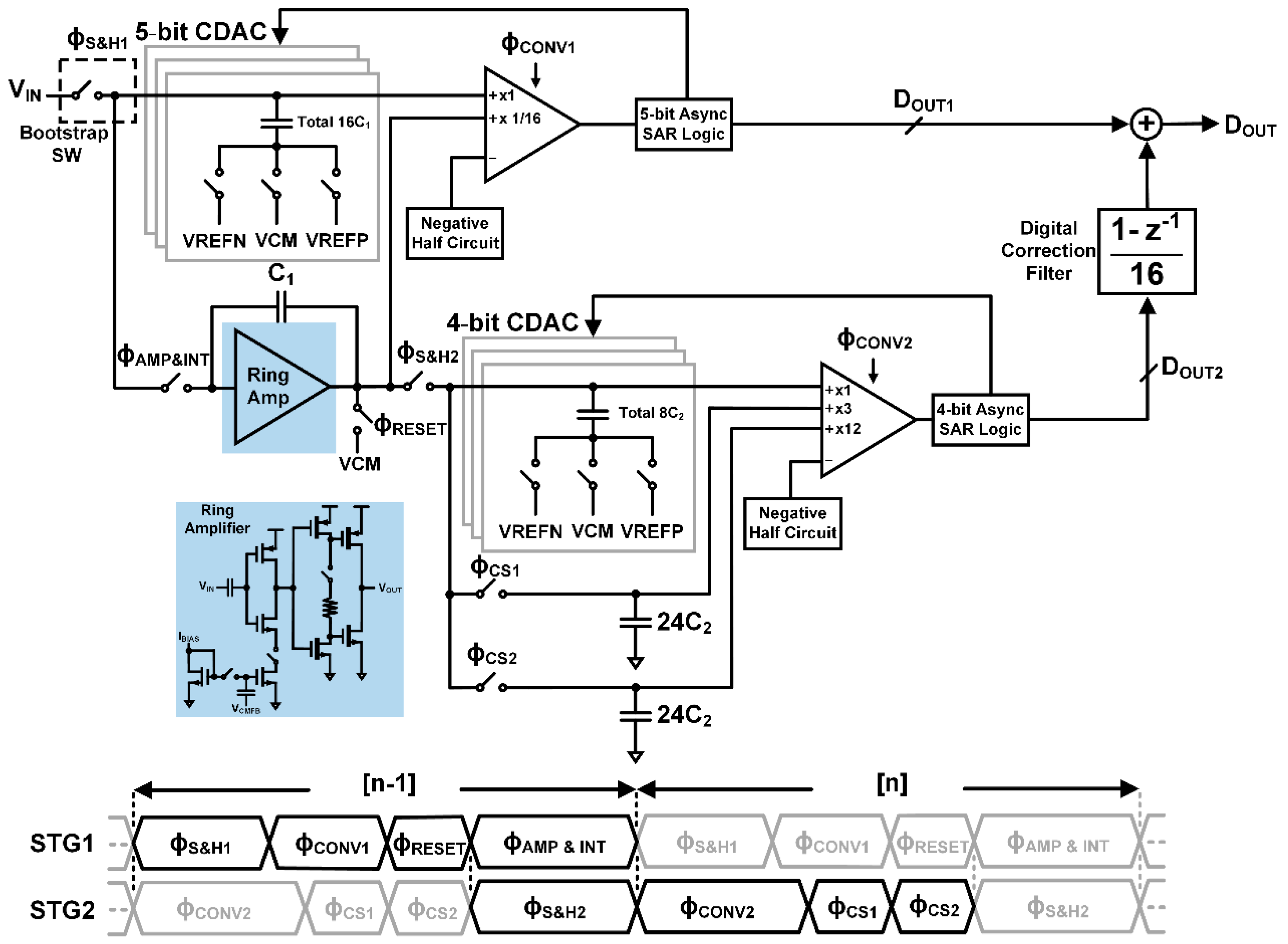
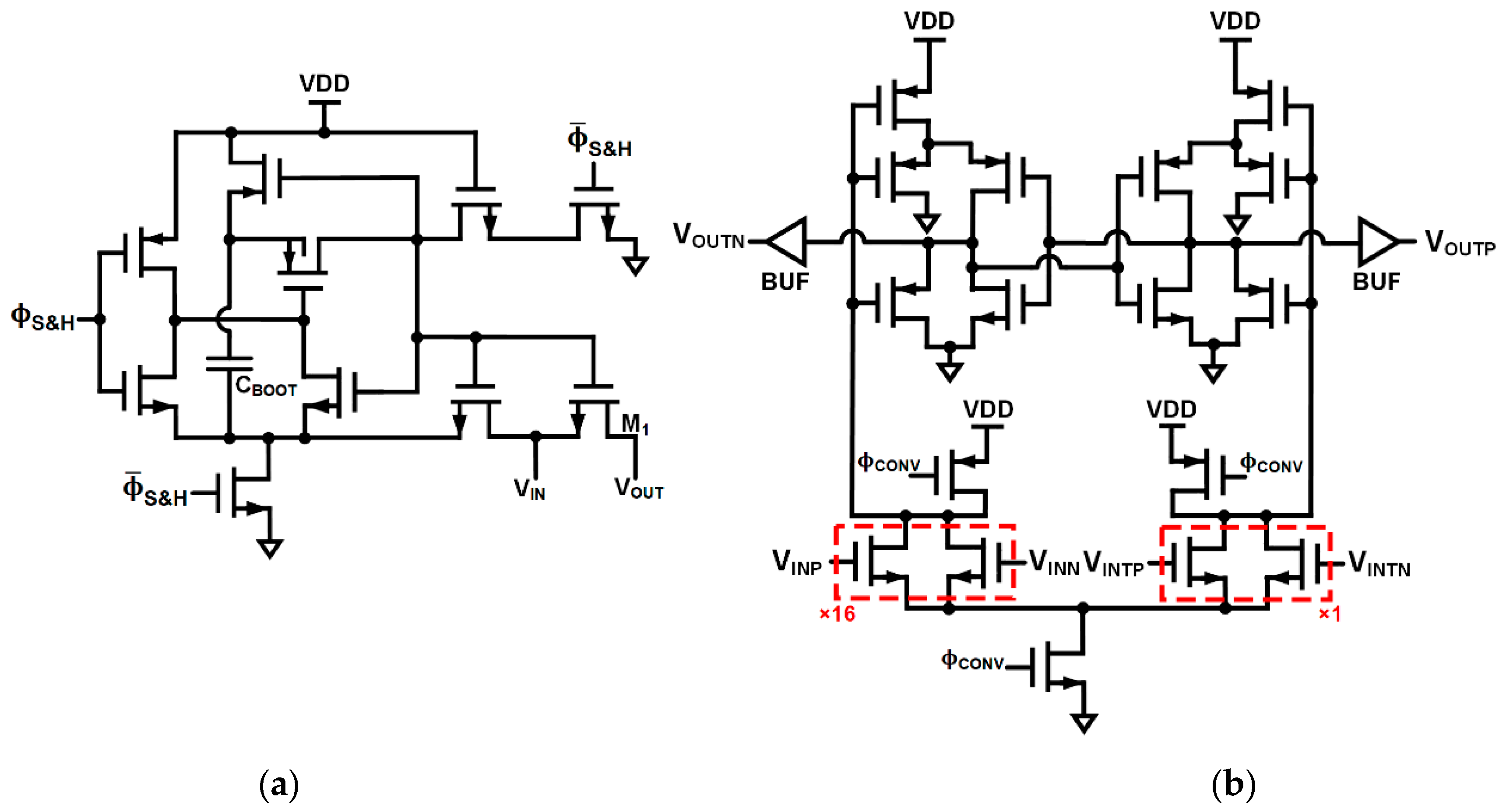
3. Circuit Implementation

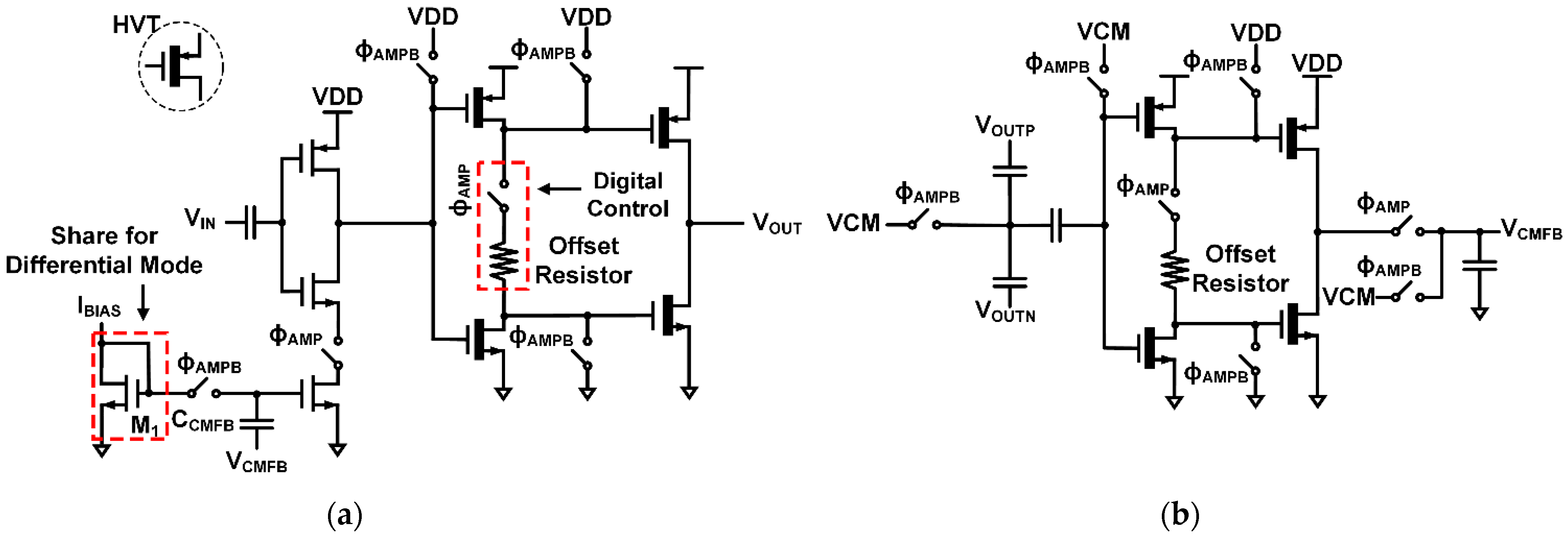
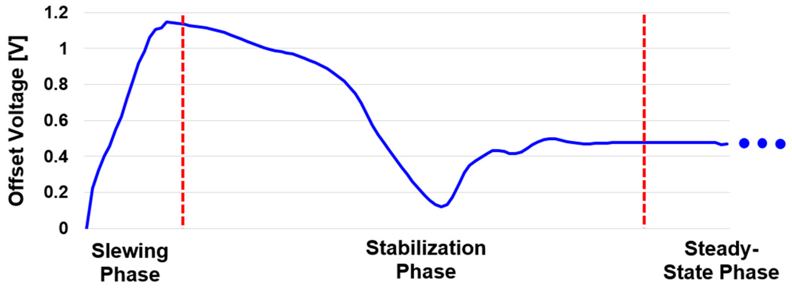
3.1. Ring Amplifier-Based Loop Filter

A ring amplifier is highly suitable for implementing the inter-stage amplifier. However, if an appropriate offset voltage is not applied due to nonideality, such as a PVT variation, the output pole movement does not provide sufficient phase margin, so oscillation or output signal settling cannot be performed properly. Therefore, the ring amplifier structure of Figure 6a is used for stable operation. A tail current device is added to the 1st stage, the 2nd and 3rd stages comprise high-threshold voltage (HVT) transistors, and a resistor is used for offset voltage generation. By using HVT transistors at the last stage, the applicable offset voltage range and output resistance can be further increased [28]. If the sum of the threshold voltages ( V TH ) of the output stage PMOS and NMOS devices is very large and exceeds the supply voltage (VDD) of the amplifier, the last stage can operate in a weak inversion region even without applying the offset voltage. As a result, the ring amplifier structure may be further simplified, but an offset resistor is still applied to prevent the case where the sum of V TH is not greater than the VDD of the amplifier due to any variation [29]. By generating the offset voltage using an IR drop through the resistor, stable operation of the ring amplifier is possible without it being affected by PVT variation. However, to prevent gain reduction of the 2nd stage due to the resistor, the 2nd stage also uses HVT devices to compensate for the decrease in gain [28]. The ring amplifier shows an open loop gain of 62 dB in simulation, so the SNDR of the proposed ADC is tolerant to the open loop gain variation without the help of digital filter calibration. The slewing and stabilization phase accounts for 30% of the amplification duration. Simulation shows that the proposed ring amplifier is 40% faster than a conventional two-stage op-amp with the same power budget and achieves a larger open-loop gain. Figure 7 shows the transient of the offset voltage during amplification. The offset voltage fluctuates rail-to-rail during slewing and stabilization phase, and it becomes constant as the amplifier enters the steady state. A large offset voltage in the steady state is often better for fast settling with decreased accuracy. However, if a large offset voltage is required to enable the size of the resistor to be increased, an additional pole may be created in the 2nd stage and speed can be reduced. Therefore, the application of an appropriate offset resistor is critical. Figure 8a contains a graph showing the change in signal-to-noise ratio (SNR) and total harmonic distortion (THD) according to the offset resistor size. When using a resistor of 3 3 . 5   k Ω , it is possible to minimize the decrease in settling speed and improve the SNR and THD performance. In addition, when the offset resistor is 3 3 . 5   k Ω , the ring amplifier can achieve 98–99% accuracy compared to when the ideal one is used. This gain error does not affect the overall ADC resolution.
Regarding the noise of the ring amplifier, the 1st stage inverter is the main noise source. To reduce thermal noise generated in the 1st stage, g m of the 1st stage devices should be increased. In the case of a ring amplifier, the minimum length device is used because it has the same characteristics as a digital circuit, so noise is suppressed by increasing the transistor width for higher g m . The input-referred noise of the ring amplifier integrated from 100 KHz to 5.2 MHz is approximately 8   n / V 2   Hz , which is small enough to not affect the overall system resolution. As shown in Figure 8b, even if the supply voltage changes by ~ 50   mV based on 1.2 V, it can be confirmed that the SNR and THD performances of the amplifier are maintained at 60 dB or more, regardless of noise and linearity. The reset switch of each stage, offset resistor, and tail current device operate only during the amplification phase ( ϕ AMP ) to minimize power consumption. In high-gain amplifiers, CM output voltage is very vulnerable to PVT variation. If not precisely defined, the CM output voltage may reach the supply rail and the PLNS-SAR ADC would malfunction. Therefore, a CMFB (common-mode feedback) circuit is necessary for the proposed ring amplifier, and is shown in Figure 6b. For accurate CMFB operation, an active type composed of a 2-stage inverter is used rather than a passive type, and it is composed of a reset switch and a capacitor to detect changes in the CM voltage. A CMFB circuit has sufficient gain and uses an HVT device and offset resistor to operate stably. The conventional active-type CMFB circuit increases accuracy through large gain, but this leads to lower CMFB bandwidth [29]. In the case of configuring CMFB through multiple loops or multiple stages [30], the accuracy is high, but design complexity increases, and the advantages of ring-amplifier power efficiency and speed are attenuated. In the proposed CMFB system, a constant voltage is charged to C CMFB according to the desired bias current through a diode connected to M 1 in Figure 6a during the nonamplification phase ( ϕ AMPB ). Subsequently, during the phase ϕ AMP , the ring amplifier operates according to the voltage on C CMFB and a CM output voltage appears. When the CM output voltage changes, the amount of change is amplified through the circuit of Figure 6b, and the amplified voltage V CMFB is quickly fed back to the 1st stage through C CMFB . Through this circuit, it is possible to quickly and accurately perform CMFB using a single CMFB loop. Consequently, the design complexity is low and power consumption can be minimized.
The switch logic of a loop filter for operation as an integrator should be different from the logic of a conventional amplifier, and is shown in Figure 9. First, when the conversion of the ( n 1 ) th sample in the 1st stage is finished, as shown in Figure 9a, during the amplification phase ( ϕ AMP ), the charge for residual voltage in the 1st stage CDAC ( CDAC 1 ) is transferred to the feedback capacitor ( C F ), and amplification and integration are performed at the same time. At this time, the 2nd stage CDAC ( CDAC 2 ) is connected to the load of the ring amplifier, and input sampling of the 2nd stage proceeds simultaneously ( ϕ S & H 2 ). CMFB is also performed in the ϕ AMP , and V CMFB , reflecting the change in the CM output voltage, is fed back through C CMFB . The conventional ring amplifier resets all nodes to common-mode voltage (VCM) as soon as the amplification process is finished. However, although the output signal of the integrator is sampled by CDAC 2 , the integrator output is also necessary for noise-shaping when performing the n th SAR conversion after sampling the n th input in the 1st stage. Therefore, after the end of ϕ AMP , to maintain the output voltage of the ring amplifier ( V OUT ) connected to the 1st multi-input comparator (1st CMP), without resettling all nodes, we separate CDAC 1 and CDAC 2 , as shown in Figure 9b, and keep the input voltage of the ring amplifier and the voltage of C F . Because the CM output voltage has already been stabilized at this time, C CMFB charges a constant voltage according to the bias current through M1 (Figure 6a). After the n th SAR conversion, V RES must be amplified and integrated again. For this purpose, all input and output voltages of the ring amplifier are reset to VCM, as shown in Figure 9c. At this time, C F can maintain the integrated signal because one side is open.

3.2. Ring Amplifier-Based Pipelined Noise-Shaping SAR ADC
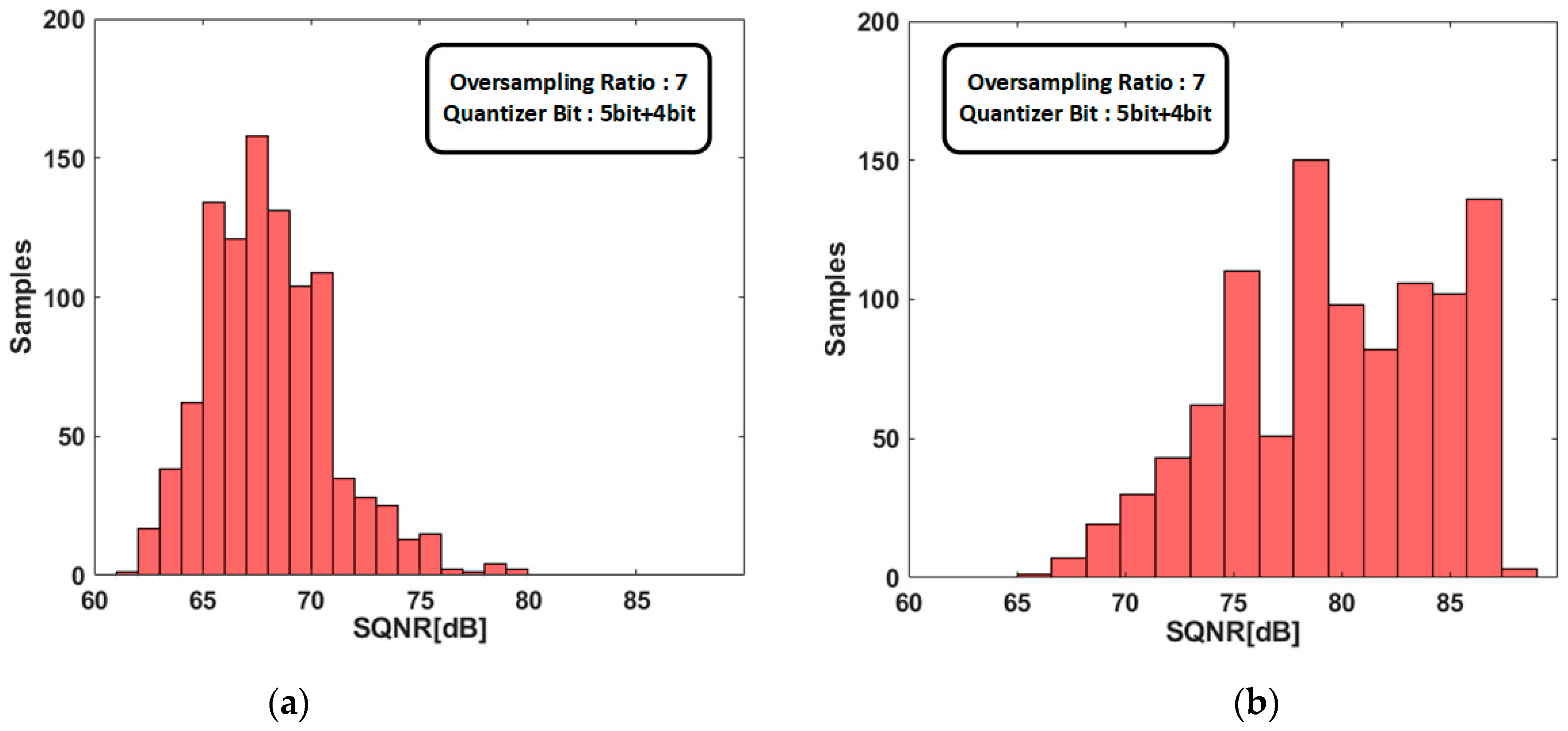
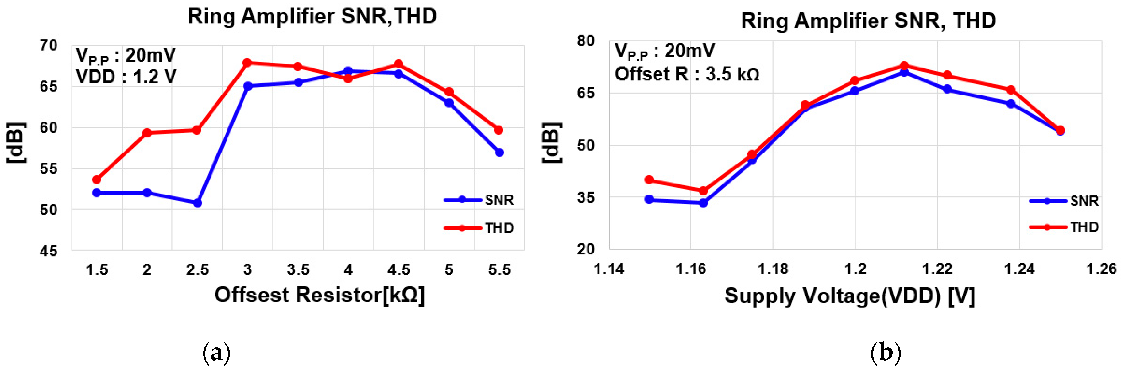
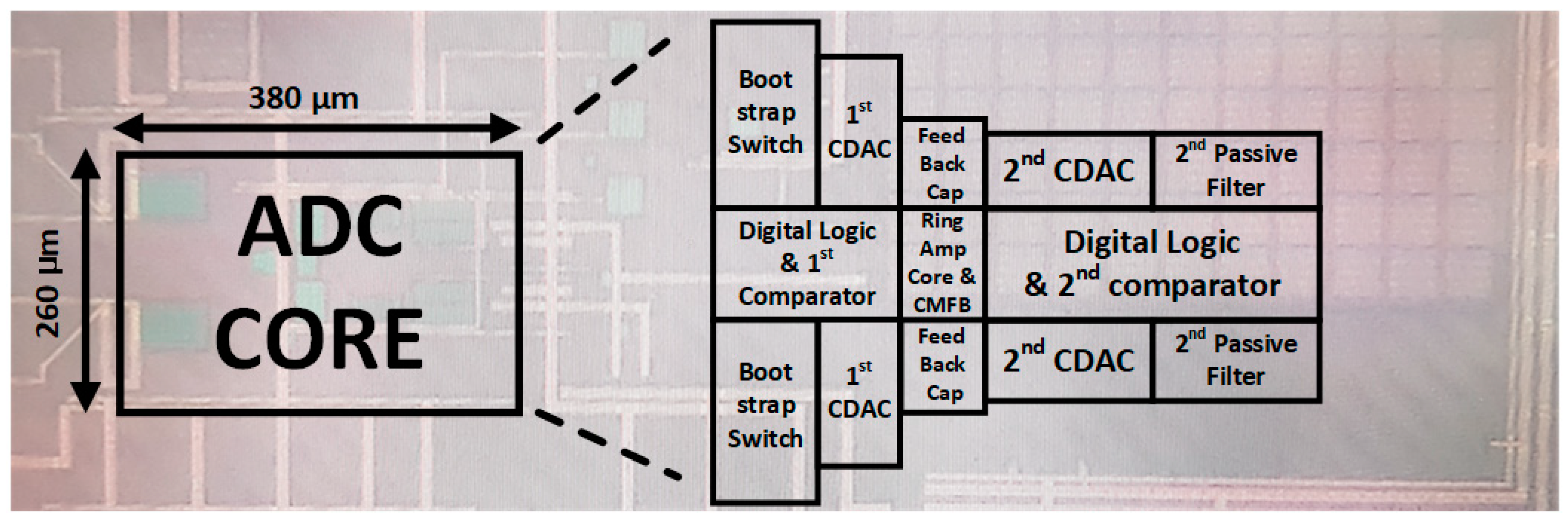
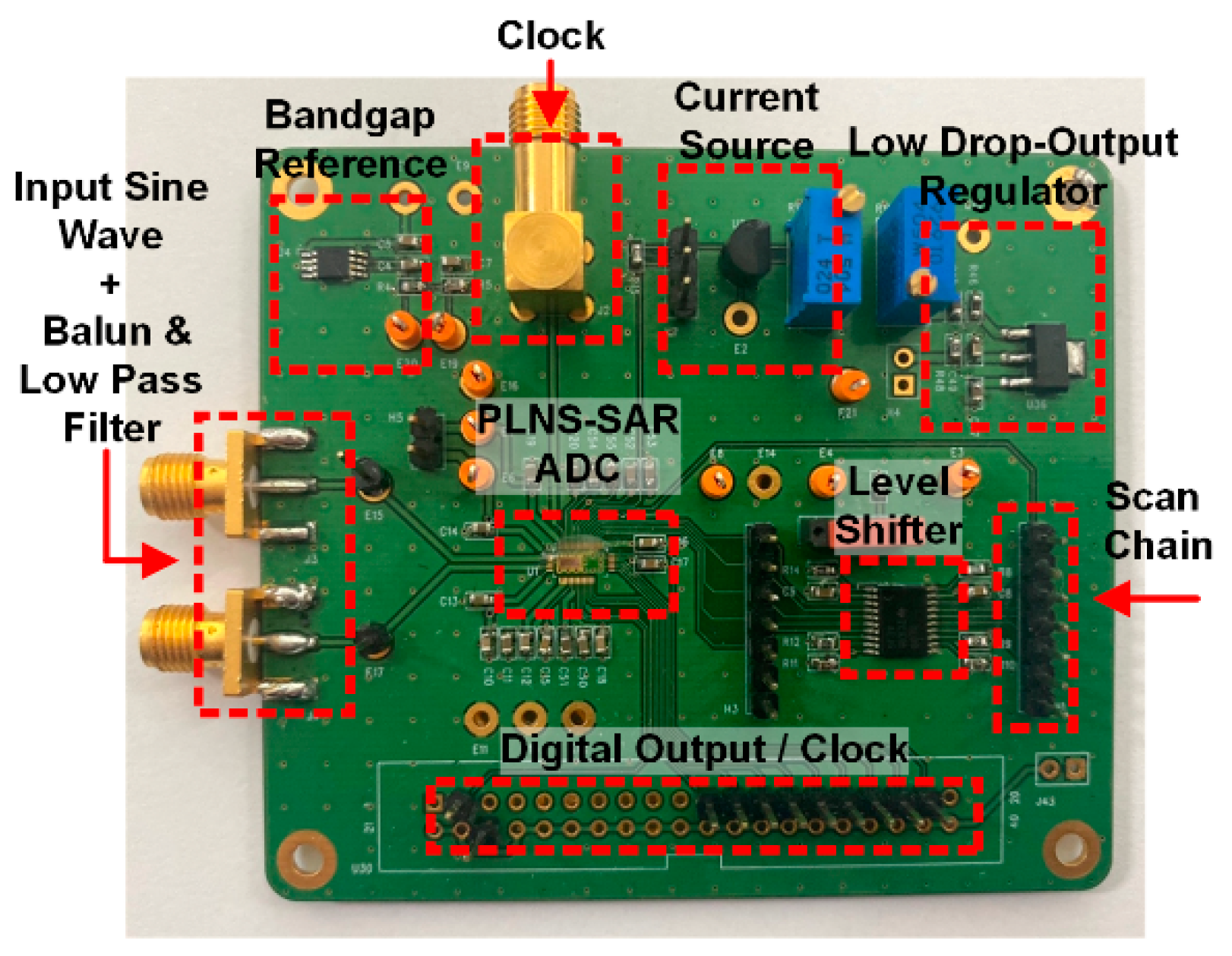
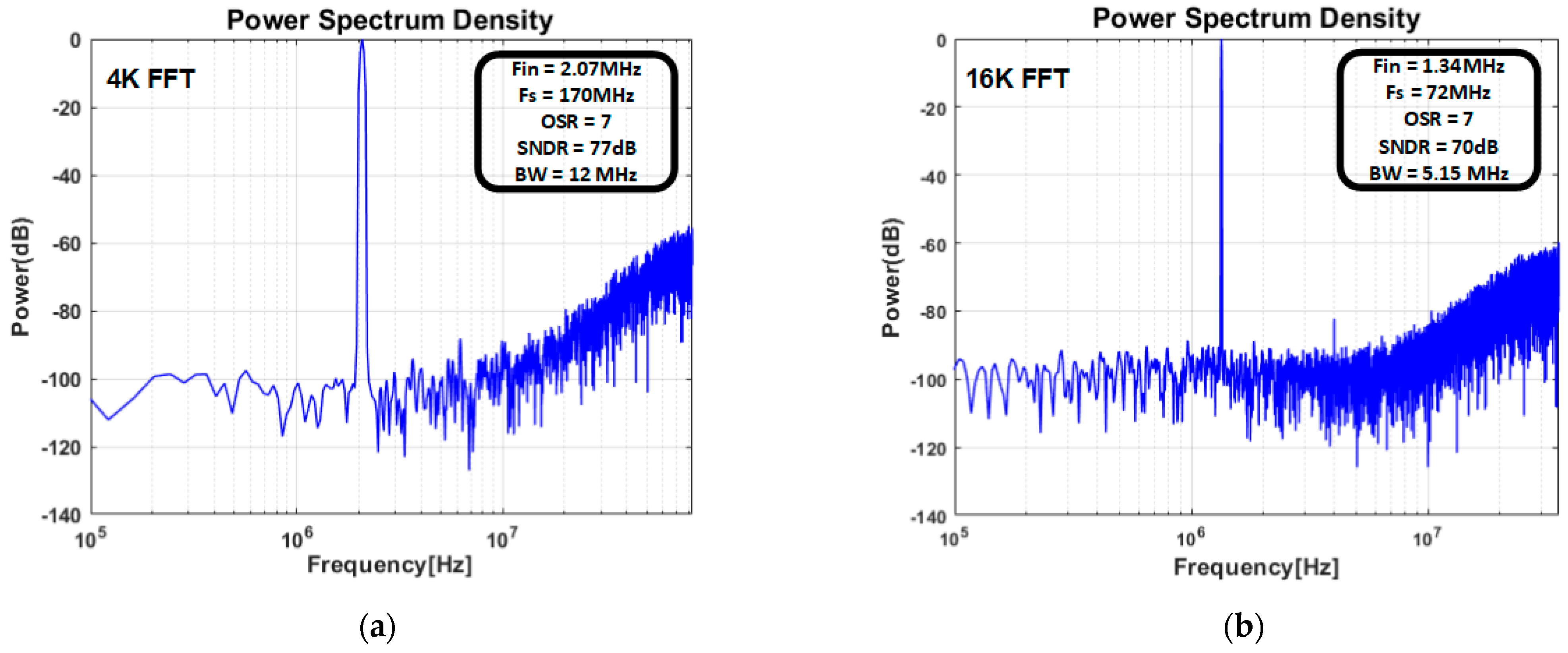
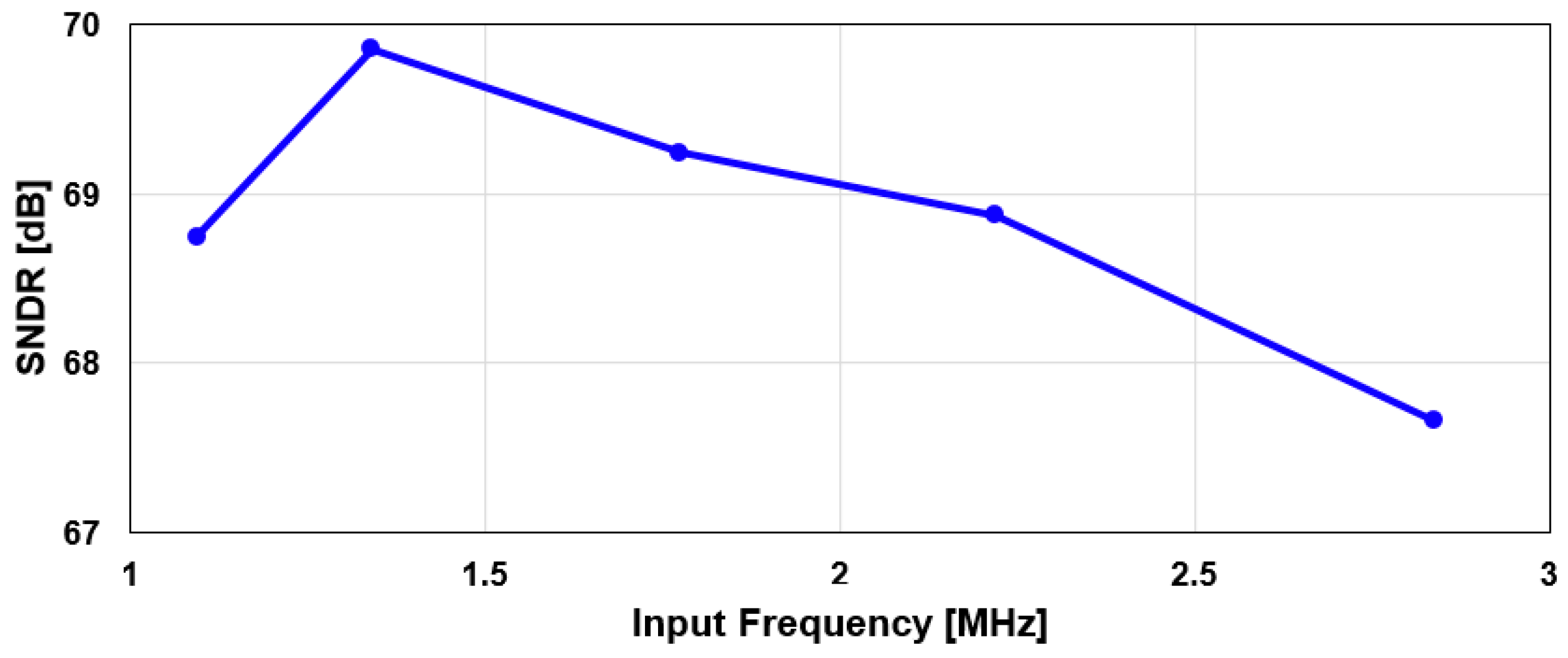
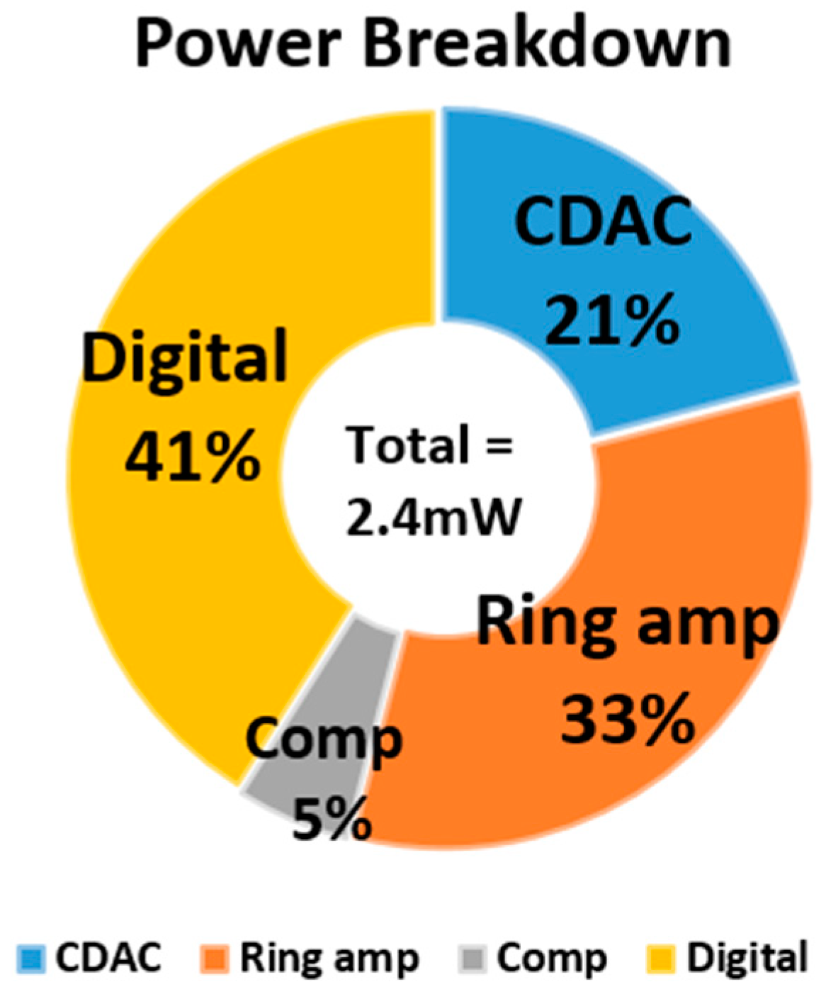
The whole system and timing diagram are shown in Figure 10 [16,17], where the ring amplifier is applied. The CDAC of each stage operates by VCM-based switch logic. The 1st stage is a 5-bit noise-shaping SAR ADC, and the 2nd stage is a 4-bit noise-shaping SAR ADC. The operation begins with the input voltage being sampled in the 1st stage ( ϕ S & H 1 ). Subsequently, after the 5-bit SAR conversion operation is performed ( ϕ CONV 1 ), the output of the ring amplifier is reset ( ϕ RESET ). After the conversion and reset process, the residual voltage is amplified and integrated simultaneously through the ring amplifier ( ϕ AMP & INT ). The duration for ϕ AMP & INT accounts for about 60% of the total sampling period. Through this, the 1st order NTF of ( 1     z 1 ) , based on the cascade-of-integrators feed forward (CIFF) structure, is implemented by the 1st stage. Simultaneously, the 2nd stage input sampling process proceeds, and the output of the amplifier is used as the 2nd stage input ( ϕ S & H 2 ). Afterward, the 2nd order NTF of ( 1     0 . 75 1 ) 2 is implemented through the 2-step charge-sharing operation ( ϕ CS 1 , 2 ) after the 4-bit SAR conversion operation ( ϕ CONV 2 ). Finally, the final output D OUT is obtained after digital correction filtering.
Because this ADC aims at high resolution, the sampling of the 1st stage must be very linear, and for this reason, the sampling switch uses a bootstrap switch for constant turn-on resistance. Figure 11a shows the circuit implementation of the bootstrap switch [31,32]. During the nonsampling phase ( ϕ S & H ) , C BOOT is charged with a voltage equal to VDD. The charged capacitor acts as a battery between the gate and source of M 1 during the sampling phase ( ϕ S & H ) . Through this, by maintaining the V GS V TH of M 1 at VDD, the turn-on resistance can be made constant and high linearity can be achieved despite fast sampling. CDAC 1 has the total capacitance of 2.3 pF (single-ended) to minimize the effect of kT/C noise. The inter-stage gain is set to 16 to avoid signal over-range and, for this, the feedback capacitor uses 143.75 fF, which is 1/16 of CDAC 1 . CDAC 2 has a smaller capacitance of ~140 fF (single-ended), and the kT/C noise of CDAC 2 can be greatly reduced through the pipelined structure and noise-shaping, so it minimally affects the resolution. Each stage comparator uses a two-stage dynamic comparator structure [33,34,35]. Figure 11b displays the circuit implementation of a multi-input comparator used in the 1st stage. An additional comparator input pair is used to attenuate and sum the integrator output with the input signal. In the 2nd stage, there are two more input pairs, and the size ratio of the input pairs is different, but the same structure is used as in the 1st stage. The 1st stage comparator input pair has a 16:1 size ratio, and the 2nd stage has a 1:3:12 size ratio for the CIFF-based NTF implementation [36]. In the case of the 2nd stage loop filter, NTF is implemented using charge-sharing by capacitor and passive gain. A passive gain is used to compensate for signal attenuation due to charge-sharing. The passive gain is implemented by adjusting the input MOS size ratio of the multi-input comparator. This compensates for signal attenuation. Although all comparators have multi-input pairs, the noise has little effect because it is attenuated by filter matching and noise-shaping. The multi-input comparator is designed considering only the speed and power consumption, and a two-stage dynamic comparator structure, which is power-efficient and has little offset, is adopted. Therefore, the comparator does not affect the overall ADC speed and the amplification phase is the speed bottleneck. Finally, the 3rd-order noise-shaping PLNS-SAR system is implemented.

4. Results

The proposed ADC was designed and fabricated using a 65 nm CMOS process. Figure 12 shows a die photograph of the ADC core. The total core area is 380 μm by 260 μm. The active area includes two noise-shaping SAR ADCs and a ring amplifier. The metal line routing of the residual signal is minimized by placing a ring amplifier between each stage. Figure 13 displays a printed-circuit-board (PCB) for evaluating and measuring performance of the proposed ADC. Included are a bandgap reference, low-dropout regulator, and current source for supply and reference voltages, in addition to a level shifter and clock connector for connection with the FPGA board in charge of digital control. Additionally, there is an input connector for supplying a sine wave that has passed through a balun and low pass filter (LPF), and a connector for checking the digital output/clock is placed on the PCB. A clean differential sine-wave input signal is supplied to the prototype through the balun and LPF, and the final digital output is obtained by a logic analyzer through a digital output connector.
Figure 14a,b shows plots of the post-layout simulation power spectral density and measured power spectral density when filter calibration is not performed. Through post-layout simulation, it can be confirmed that a SNDR of 77 dB is achieved for a BW of 12 MHz with a Fs of 170 MHz and an oversampling ratio (OSR) of 7. A resolution close to 80 dB and over 10 MHz BW without filter calibration is still attainable. A high resolution and wide BW can be achieved simultaneously through the PLNS-SAR ADC using a ring amplifier. Through measurement, the SNDR of 70 dB with a 5.2 MHz BW (Fs of 72 MHz and OSR of 7) is achieved. A degradation in the resolution and BW is observed compared to the post-layout simulation results, and it is presumably caused by a reset problem in the ring amplifier. The short reset phase is easily affected by PVT variation and insufficient reset time could deteriorate the quality of the integrator output while decreasing both the speed and accuracy. Nevertheless, a wide BW of 5 MHz or more is still maintained, and a resolution of 70 dB can be achieved without filter calibration. Figure 15 shows the measured SNDR versus input frequency, and the SNDR degradation is less than 3 dB. Figure 16 shows the power consumption chart by block, with a total power consumption of 2.4 mW. The most power-hungry block of the conventional PLNS-SAR ADC [16] is the inter-stage amplifier implemented with an OTA, accounting for more than half of the total power consumption. However, the ring amplifier in this work consumes only approximately 0.8 mW, and the total power consumption is reduced by more than 30% compared to [16]. With the measured SNDR and bandwidth presented above, the reduced power consumption provides an FoM S ,   SNDR ( = SNDR + 10 log 10 BW / Power ) of 163.5 dB, which demonstrates good power efficiency.

5. Conclusions

This work demonstrates a proposed ADC that was designed and fabricated using a 65 nm CMOS process. Using the PLNS-SAR ADC structure, it is possible to implement a high resolution without being subject to comparator design requirements. The inter-stage amplifier and integrator are implemented by a ring amplifier. Using the ring amplifier, the power consumption is reduced by 30% compared to the conventional PLNS-SAR ADC power consumption. Using the high-gain ring amplifier, noise leakage is minimized and a structure tolerant of filter mismatch is implemented. The proposed PLNS-SAR ADC can achieve high resolution, wide BW, and good power efficiency using the ring amplifier without filter calibration.

Author Contributions

Conceptualization, J.L. and H.C.; methodology, J.L.; software, J.L. and S.L.; validation, J.L.; formal analysis, J.L.; investigation, J.L. and S.L.; resources, H.C.; data curation, J.L.; writing—original draft preparation, J.L.; writing—review and editing, J.L. and H.C.; visualization, J.L. and K.K.; supervision, J.L. and H.C.; project administration, H.C.; funding acquisition, H.C. All authors have read and agreed to the published version of the manuscript.

Funding

This research was supported by the National Research Foundation of Korea, grant number 2020R1A2C1099786.

Acknowledgments

The EDA Tool was supported by the IC Design Education Center.

Conflicts of Interest

The authors declare no conflict of interest.

References

  1. Ron, K.; Shen, J.; Decker, S.; Li, H.; Ibaragi, E.; Zhu, H. A 14 b 80 MS/s SAR ADC with 73.6 DB SNDR in 65 nm CMOS. IEEE J. Solid State Circuits 2013, 48, 3059–3066. [Google Scholar]
  2. Lee, K.; Miller, R.M.; Temes, C.G. An 8.1 mW, 82 dB delta-sigma ADC with 1.9 MHz BW and −98 dB THD. IEEE J. Solid State Circuits 2009, 44, 2202–2211. [Google Scholar] [CrossRef]
  3. Chandrakasan, P.A.; Verma, N. An ultra low energy 12-bit rate-resolution scalable SAR ADC for wireless sensor nodes. IEEE J. Solid State Circuits 2009, 42, 1196–1205. [Google Scholar]
  4. Maddox, M.; Chen, B.; Coln, M.; Kapusta, R.; Shen, J.; Fernando, L. A 16 bit linear passive-charge-sharing SAR ADC in 55 nm CMOS. In Proceedings of the IEEE Asian Solid-State Circuits Conference, Toyama, Japan, 7–9 November 2016. [Google Scholar]
  5. Flynn, P.M.; Lee, C. A SAR-assisted two-stage pipeline ADC. IEEE J. Solid State Circuits 2011, 46, 859–869. [Google Scholar]
  6. Liu, Q.; Shu, W.; Chang, J. A 1-GS/s 11-Bit SAR-assisted pipeline ADC with 59-dB SNDR in 65-nm CMOS. IEEE Trans. Circuits Syst. II Express Briefs 2018, 65, 1164–1168. [Google Scholar] [CrossRef]
  7. Yang, C.; Li, F.; Li, W.; Wang, X.; Wang, Z. An 85 mW 14-bit 150 MS/s pipelined ADC with 71.3 dB peak SNDR in 130nm CMOS. In Proceedings of the IEEE Asian Solid-State Circuits Conference, Singapore, 11–13 November 2013. [Google Scholar]
  8. Verbruggen, B.; Iriguchi, M.; Craninckx, J. A 1.7 mW 11 b 250 MS/s 2× interleaved fully dynamic pipelined SAR ADC in 40nm digital CMOS. In Proceedings of the IEEE International Solid-State Circuits Conference, San Francisco, CA, USA, 19–23 February 2012. [Google Scholar]
  9. Lee, C.; Venkatachala, P.; ElSHater, A.; Xiao, B.; Hu, H.; Moon, U. Cascoded ring amplifiers for high speed and high accuracy settling. In Proceedings of the IEEE International Symposium on Circuits and Systems, Sapporo, Japan, 26–29 May 2019. [Google Scholar]
  10. Verbriggen, B.; Deguchi, K.; Malki, B.; Craninckx, J. A 70 dB SNDR 200 MS/s 2.3 mW dynamic pipelined SAR ADC in 28nm digital CMOS. In Proceedings of the Symposium on VLSI Circuits Digest of Technical Papers, Honolulu, HI, USA, 10–13 June 2014. [Google Scholar]
  11. Tripathi, V.; Murmann, B. A 160 MS/s, 11.1 mW, single-channel pipelined SAR ADC with 68.3 dB SNDR. In Proceedings of the IEEE Custom Integrated Circuits Conference, San Jose, CA, USA, 15–17 September 2014. [Google Scholar]
  12. Liu, H.; Liu, M.; Zhu, Z. A 12-bit 200MS/s Pipelined-SAR ADC in 65-nm CMOS with 61.9 dB SNDR. In Proceedings of the IEEE International Conference on Electron Devices and Solid-State Circuits, Xi’an, China, 12–14 June 2019. [Google Scholar]
  13. Chen, Y.; Wang, J.; Hu, H.; Ye, F.; Ren, J. A 200 MS/s, 11 bit SAR-assisted pipeline ADC with bias-enhanced ring amplifier. In Proceedings of the IEEE International Symposium on Circuits and Systems, Baltimore, MD, USA, 28–31 May 2017. [Google Scholar]
  14. Frendenburg, J.; Flynn, M. A 90-MS/s 11-MHz-bandwidth 62-dB SNDR noise-shaping SAR ADC. IEEE J. Solid State Circuits 2012, 47, 2898–2904. [Google Scholar] [CrossRef]
  15. Liu, C.; Huang, M. 28.1 A 0.46 mW 5 MHz-BW 79.7 dB-SNDR noise-shaping SAR ADC with dynamic-amplifier-based FIR-IIR filter. In Proceedings of the IEEE International Solid-State Circuits Conference, San Francisco, CA, USA, 5–9 February 2017. [Google Scholar]
  16. Oh, S.; Oh, Y.; Lee, J.; Kim, K.; Lee, S.; Kim, J.; Chae, H. A 80 dB DR 6 MHz bandwidth pipelined noise-shaping SAR ADC with 1–2 MASH structure. In Proceedings of the IEEE Custom Integrted Circuits Conference, Boston, MA, USA, 22–25 March 2020. [Google Scholar]
  17. Oh, S.; Oh, Y.; Lee, J.; Kim, K.; Lee, S.; Kim, J.; Chae, H. A 85 dB DR 4 MHz BW pipelined noise-shaping SAR ADC with 1-2 MASH structure. IEEE J. Solid State Circuits 2021, 1. [Google Scholar] [CrossRef]
  18. Gao, B.; Li, X.; Yan, C.; Wu, J. Active noise shaping SAR ADC based on ISDM with the 5MHz bandwidth. In Proceedings of the IEEE International Symposium on Circuits and Systems, Seville, Spain, 12–14 October 2020. [Google Scholar]
  19. Chen, Z.; Miyahara, M.; Matsuzawa, A. A 2nd order fully-passive noise-shaping SAR ADC with embedded passive gain. In Proceedings of the IEEE Asian Solid-State Circuits Conference, Toyama, Japan, 7–9 November 2016. [Google Scholar]
  20. Chen, Z.; Miyahara, M.; Matsuzawa, A. A 9.35-ENOB, 14.8 fJ/conv.-step fully-passive noise-shaping SAR ADC. In Proceedings of the IEEE Symposium on VLSI Circuits, Kyoto, Japan, 17–19 June 2015. [Google Scholar]
  21. Maghami, H.; Payandehnia, P.; Mirzaie, H.; Mayaram, K.; Zanbaghi, R.; Fiez, T. A highly linear OTA-free VCO-based 1-1 MASH ΔΣ ADC. In Proceedings of the IEEE International Symposium on Circuits and Systems, Baltimore, MD, USA, 28–31 May 2017. [Google Scholar]
  22. Zhang, S.; Zhu, Z.; Zhang, H.; Xiong, Z.; Li, Q. A 90-dB DC gain high-speed nested gain-boosted folded-cascode opamp. In Proceedings of the 11th Conference on Ph.D. Research in Microelectronics and Electronics, Glasgow, UK, 29 June–2 July 2015. [Google Scholar]
  23. Rahim, S.; Azmi, I. A CMOS single stage fully differential folded cascode amplifier employing gain boosting technique. In Proceedings of the International Symposium on Integrated Circuits, Singapore, 12–14 December 2011. [Google Scholar]
  24. Park, Y.; Song, J.; Choi, Y.; Lim, C.; Ahn, S.; Kim, C. An 11-b 100-MS/s fully dynamic pipelined ADC using a high-linearity dynamic amplifier. IEEE J. Solid State Circuits 2020, 55, 2468–2477. [Google Scholar] [CrossRef]
  25. Malki, B.; Verbruggen, B.; Wambacq, P.; Deguchi, K.; Iriguchi, M.; Craninckx, J. A complementary dynamic residue amplifier for a 67 dB SNDR 1.36 mW 170 MS/s pipelined SAR ADC. In Proceedings of the 40th European Solid State Circuits Conference, Venice Lido, Italy, 22–26 September 2014. [Google Scholar]
  26. Sehgal, R.; Goes, F.; Bult, K. A 13-mW 64-dB SNDR 280-MS/s pipelined ADC using linearized integrating amplifiers. IEEE J. Solid State Circuits 2018, 53, 1878–1888. [Google Scholar] [CrossRef]
  27. Hershberg, B.; Weaver, S.; Sobue, K.; Takeuchi, S.; Hamashita, K.; Moon, U. Ring amplifiers for switched-capacitor circuits. In Proceedings of the IEEE International Solid-State Circuits Conference, San Francisco, CA, USA, 19–23 February 2012. [Google Scholar]
  28. Lim, Y.; Flynn, M. 11.5 A 100 MS/s 10.5 b 2.46 mW comparator-less pipeline ADC using self-biased ring amplifiers. In Proceedings of the IEEE International Solid-State Circuits Conference Digest of Technical Paper, San Francisco, CA, USA, 9–13 February 2014. [Google Scholar]
  29. Lagos, J.; Hershberg, B.; Martens, E.; Wambacq, P.; Craninckx, J. A single-channel, 600 Msps, 12 bit, ringamp-based pipelined ADC in 28 nm CMOS. In Proceedings of the Symposium on VLSI Circuits, Kyoto, Japan, 5–8 June 2017. [Google Scholar]
  30. Hershberg, B.; Dermit, D.; Liempd, B.; Martens, E.; Markulic, N.; Lagos, J.; Craninckx, J. A 3.2 GS/s 10 ENOB 61mW ringamp ADC in 16 nm with background monitoring of distortion. In Proceedings of the IEEE International Solid-State Circuits Conference, San Francisco, CA, USA, 17–21 February 2019. [Google Scholar]
  31. Liu, C.; Chang, S.; Huang, G.; Lin, Y. A 10-bit 50-MS/s SAR ADC with a monotonic capacitor switching procedure. IEEE J. Solid State Circuits 2010, 45, 731–740. [Google Scholar] [CrossRef]
  32. Aksin, D.; Al-Shyoukh, M.; Maloberti, F. Switch bootstrapping for precise sampling beyond supply voltage. IEEE J. Solid State Circuits 2006, 41, 1938–1943. [Google Scholar] [CrossRef] [Green Version]
  33. Chiu, P.; Zimmer, B.; Nikolić, B. A double-tail sense amplifier for low-voltage SRAM in 28 nm technology. In Proceedings of the IEEE Asian Solid-Stage Circuits Conference, Toyama, Japan, 7–9 November 2016. [Google Scholar]
  34. Miyahara, M.; Asada, Y.; Paik, D.; Matsuzawa, A. A low-noise self-calibrating dynamic comparator for high-speed ADCs. In Proceedings of the IEEE Asian Solid-Stage Circuits Conference, Fukuoka, Japan, 3–5 November 2008. [Google Scholar]
  35. Babayan-M, S.; Lotfi, R. Analysis and design of a low-voltage low-power double-tail comparator. IEEE Trans. Very Large Scale Integr. Syst. 2014, 22, 343–352. [Google Scholar] [CrossRef]
  36. Liu, J.; Li, S.; Guo, W.; Wen, G.; Sun, N. A 0.0029 mm2 17 fJ/conversion-step third-order CT ΔΣ ADC with a single OTA and second-order noise-shaping SAR quantizer. IEEE J. Solid State Circuits 2019, 54, 428–440. [Google Scholar] [CrossRef]
Figure 1. The conventional pipelined SAR ADC block diagram.
Electronics 10 01968 g001
Figure 2. The pipelined noise-shaping SAR ADC block diagram.
Electronics 10 01968 g002
Figure 3. The SQNR histogram for different open-loop gain of inter-stage amplifier with 5% variation and no filter calibration: (a) the open-loop gain of 40 dB and (b) the open-loop gain of 60 dB.
Electronics 10 01968 g003
Figure 4. The implementation of inter-stage gain using (a) the folded cascode op-amp in closed-loop and (b) the dynamic amplifier in open-loop.
Electronics 10 01968 g004
Figure 5. The conventional ring amplifier structure with three inverters (single-ended view) and its transient response (differential mode).
Electronics 10 01968 g005
Figure 6. (a) The proposed ring amplifier structure in the single-ended mode. (b) The CMFB circuit with a single loop.
Electronics 10 01968 g006
Figure 7. The transient of the offset voltage during amplification.
Electronics 10 01968 g007
Figure 8. The SNR and THD of ring amplifier versus (a) the offset resistor and (b) the supply voltage.
Electronics 10 01968 g008
Figure 9. The ring amplifier-based integrator and its three phases of (a) amplification, (b) nonamplification without reset, and (c) nonamplification with reset; and (d) the operation timing diagram.
Electronics 10 01968 g009
Figure 10. The circuit implementation of the proposed ADC and its operation timing diagram.
Electronics 10 01968 g010
Figure 11. The schematic of (a) the bootstrap switch and (b) the multi-input two-stage dynamic comparator.
Electronics 10 01968 g011
Figure 12. The die photograph of the ADC core.
Electronics 10 01968 g012
Figure 13. The evaluation board for the proposed ADC prototype.
Electronics 10 01968 g013
Figure 14. The output power spectral density without filter calibration from (a) the post layout simulation and (b) the measurement.
Electronics 10 01968 g014
Figure 15. The measured SNDR versus input frequency.
Electronics 10 01968 g015
Figure 16. The power consumption breakdown of the proposed ADC.
Electronics 10 01968 g016
Table 1. The performance comparison of ADCs with pipelined structure.
ReferenceVLSI’14 [10]CICC’14 [11]EDSSC’19 [12]ISCAS’17 [13]
Technology28 nm CMOS65 nm CMOS65 nm CMOS40 nm CMOS
ADC TypePipeline-SARPipeline-SARPipeline-SARPipelined
Signal to Noise and Distortion Ratio (SNDR) [dB]7068.361.958
Sampling Rate (Fs) [Ms/s]200160200200
Power [mW]2.311.17.32.28
Amplifier CalibrationYesNoNoNo
Amplifier TypeDynamicOpen-loop
2-stage
CascadeRing
Publisher’s Note: MDPI stays neutral with regard to jurisdictional claims in published maps and institutional affiliations.

