Article

A Single-Amplifier Dual-Residue Pipelined-SAR ADC

School of Electrical Engineering, Korea Advanced Institute of Science and Technology (KAIST), Daejeon 34141, Korea
Electronics 2021, 10(4), 421; https://doi.org/10.3390/electronics10040421
Submission received: 13 January 2021 / Revised: 3 February 2021 / Accepted: 4 February 2021 / Published: 9 February 2021
(This article belongs to the Special Issue Advances on Analog-to-Digital and Digital-to-Analog Converters)

Abstract

:
This work presents a 12 bit 200 MS/s dual-residue pipelined successive approximation registers (SAR) analog-to-digital converter (ADC) with a single open-loop residue amplifier (RA). By using the inherent characteristics of the SAR conversion scheme, the proposed ADC sequentially generates two residue levels from the single RA, which eliminates the need for inter-stage gain-matching calibration. To convert the sequentially generated the two residues, a capacitive interpolating SAR ADC (I-SAR ADC) is also proposed. The I-SAR ADC is very compact because it consists of the one comparator, a CDAC, and control logic like a conventional SAR ADC. In addition, the I-SAR ADC needs no static power dissipation for the residue interpolation. A prototype ADC fabricated in a 40 nm CMOS technology occupies an active area of 0.026 mm2. At a 200 MS/s sampling-rate with the Nyquist input, the ADC achieves an SNDR (Signal-to-Noise distortion ratio) of 62.1 dB and 67.1 dB SFDR (Spurious-Free Dynamic Range), respectively. The total power consumed is 3.9 mW under a 0.9 V supply. Without any inter-stage mismatch calibration, the ADC achieve Walden Figure-of-Merit (FoM) of 19.0 fJ/conversion-step.

1. Introduction

Recently, high-resolution (>10 ENOB (Effective Number of Bits)) and high-speed (>150 MS/s) analog-to-digital converters (ADCs) with low power consumption have become an essential building block in modern wireless communication systems. Owing to the evolution of the CMOS process, the charge-redistribution successive-approximation-register (SAR) ADC is very attractive as a high-performance ADC [1,2,3,4,5]. However, the SAR ADC has a speed bottleneck due to the serial conversion mechanism, and it is difficult to have a high signal-to-noise ratio (SNR) due to the comparator noise.
Among the several architectural approaches, the SAR-assisted pipeline configurations have been proven a promising high-speed high-resolution ADC structure with excellent energy efficiency [6,7,8,9,10,11,12,13,14,15,16,17]. As shown Figure 1, this type of hybrid ADC uses the low-resolution energy-efficient SAR ADCs and the residue amplifiers (RAs). The ADC enhances noise performance through residue amplification and improves the effective operational conversion speed by operating in a pipeline fashion. However, the RA remains a major design challenge in terms of power, noise, and area. Even though the dynamic amplifiers recently reported in [6,7] showed remarkable power efficiency and speed, the calibration circuitry for accurate residue gain is an unavoidable overhead. Ring amplifiers [15,16] have the advantage of lower power consumption and process scalability, but the design complexity increases to achieve high DC gain for accurate inter-stage gain. To avoid the accurate gain requirement of the RA, dual-residue pipelining schemes have been proposed [17,18,19,20,21,22,23]. Because the conversion scheme uses the ratio of the two residues to find the LSB code, it is important that the two residues are amplified by the same gain value. This means that the relative gain value between the two RAs is more important than the absolute gain value. Although the requirement is relaxed because the residue amplifier is not designed with an absolute gain value, the two RAs that still need to have matched gain is another design overhead.
With the pros and cons of the previous architectural approaches, a structural consideration is needed to reduce the design complexity without the need for additional calibration logic while reducing the power burden by reducing the amplifier requirement. Hence, this paper presents a new dual-residue pipelined-SAR architecture that uses a single open-loop residue amplifier. The proposed ADC does not require any inter-stage mismatch calibration for an accurate gain. We also introduce a capacitive interpolating SAR ADC (I-SAR ADC) for the two-residue interpolation. The I-SAR ADC needs no static power consumption for the residue interpolation. A 12 b 200 MS/s prototype ADC demonstrates the feasibility of the new architecture [22].
This article is organized as follows. In Section 2, the conventional dual-residue architecture is reviewed. Section 3 introduces the proposed single-amplifier dual-residue generation technique and a capacitive interpolation SAR ADC as a low power sub-stage ADC. Section 4 shows the proposed architecture and hardware implementation. Finally, Section 5 presents the measured performance of the prototype ADC and comparison. Finally, Section 6 concludes this article.

2. Review of Dual-Residue Processing Concept

Figure 2a shows the structure of the pipelined ADC proposed in [19]. According to the result of analog-to-digital conversion performed by the first flash ADC (Flash 1), the two-residue architecture uses the differences between the input signal and the closet quantization levels (Vr+ and Vr−). In other words, the voltage levels of two residues are determined according to the input level within a full scale of 1 LSB. In addition, then, the complementary residues are amplified by two RAs (A1 and A2), respectively. Finally, the second stage (Flash 2) can determine the output code by interpolating the two amplified residues with opposite polarity. For this operation, the exact gain values of the two RAs are not as important as the conventional pipeline ADC because the relative position of the ground level is an input information. As shown in Figure 2b, the architecture operates correctly no matter what value is chosen for the inter-stage gain, provided that both residue gains match. This means that the dual-residue architecture eliminates the need for the absolute gain accuracy. Additionally, since the amplified complementary residues (the outputs of the RAs) are used to determine the LSB code from the second stage, a reference voltage is not required. However, if the amplifiers have different gains, the ADC cannot avoid performance degradation (Figure 2c). Therefore, the required gain and offset matching burden is still considerable.
Figure 3 shows the previous implementations for interpolating the two complementary residues. With the same interpolation scheme as in [19], the resistor-based (R-based) network reported in [23] can easily output multiple interpolated levels (Figure 3a). However, the R-based network requires an additional capacitor DAC (CDAC) for the pipeline operation and thus requires a large area. In addition, static power is consumed because RAs must be powered continuously for interpolation operation. In the capacitor-based (C-based) network reported in [20], the static current does not flow (Figure 3b). However, there are many switches connected to the critical node (Vra+ and Vra−). With the connection, the junction capacitance of the switches causes the linearity issue of interpolated levels. In conclusion, a new interpolation structure that has a small area but does not consume static power and does not have linearity issues is needed.

3. Proposed Architecture

Based on the earlier discussions, a new pipelined SAR architecture is proposed that uses only a single RA, which requires neither gain accuracy nor matching, allowing calibration-free open-loop RA (Figure 4). In addition, a capacitive interpolation SAR ADC for the second stage is also proposed for low power fine analog-to-digital conversion.

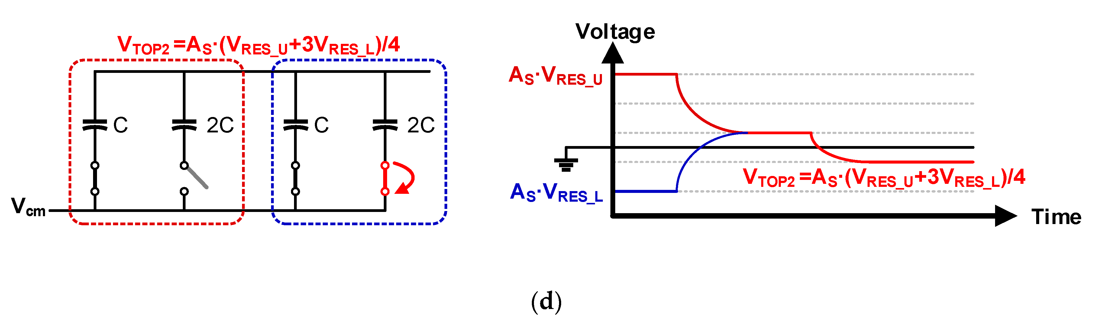
3.1. Dual-Residue Generation with a Single Amplifier

Figure 5 explains the conceptual block diagram and operation of the proposed single-amplifier dual-residue technique. As shown in Figure 5a, unlike the conventional architecture, in which two RAs that simultaneously amplify two residues, the proposed scheme is that two residues are sequentially amplified with one residue amplifier. The residue voltage waveform is demonstrated phase-by-phase in Figure 5b. After A/D conversion, the closest quantization levels (Vref(i) and Vref(i-1)) can be decided. When ΦU is enabled, VRES_U is amplified by the RA with gain of As. VRES_U represents the difference between the input signal (Vin) and the larger value among the quantization levels (Vref(i)) closest to Vin. After sampling As·VRES_U in the following stage, VRES_L is amplified and transferred. Please note that the resolution of the coarse ADC is sufficiently fine (>5 bit), a gain mismatch between the two residues rarely occurs.
Figure 6 explains the principle of the proposed single-amplifier dual-residue technique in SAR ADC. The proposed technique generates two residues sequentially by taking advantage of the SAR operation: Assuming that the LSB of the coarse decision is ‘0′, the upper residue VRES_U is generated on the first-stage CDAC when the coarse SAR conversion is completed. In the example shown in Figure 6a,b, the LSB decision is done by switching CLSB from Vcm to Vref-. When VRES_U is generated by switching CLSB, the 1st amplification (ΦU) operation is performed. To generate a lower residue, VRES_L, only 1-LSB transition of the coarse resolution is required, which can be simply done by switching the termination capacitor CTEM. As shown in Figure 6c,d, VREF_L is can be generated by switching CTEM to Vref+ from Vcm after 1st amplification. Please note that the proposed technique does not require an additional hardware burden and only requires 1 cycle of timing to generate a complementary residue. In addition, unlike the conventional scheme, the sequentially generated two residue signals are amplified by a single RA (with the gain of AS) and sampled by the second stage sequentially. This single-amplifier dual-residue technique provides inherently gain-matched residues. Thus, a simple open-loop RA can be used as long as it satisfies the required backend linearity.
However, there are other non-idealities to consider. First, the amplifier offset needs to be considered. As shown in Figure 7a, if the amplifier has an offset, two residues (VRES_U and VRES_L) are amplified by including an amplifier offset with the same polarity. Figure 7b shows the residue profile when the amplifier offset occurs. Please note that the x-axis direction means the level of the input signal at the 1st stage, and the y-axis direction means the level after amplification. From the shifted residue profile, the amplifier reduces linearity by generating missing and wide codes as well as fine code offset. Additionally, the input level may be out of the acceptable range due to disturbance such as settling error or comparator noise in the first stage ADC.
To overcome these issues, the over-ranged residue generation technique is proposed. In other words, we intentionally choose reference levels to generate the two residues with recoverable range as much as +/− 0.5 LSB scale of inter-stage redundancy. In the example shown in Figure 8a, in addition to the main CDAC, which determines the code of the 1st stage, an auxiliary CDAC for over-ranged residue generation was implemented. Since only the capacitance weight of the LSB scale is needed, the area increase is insignificant, less than 0.04% for the 12-bit prototype ADC. When the coarse conversion is done, VRES_U is generated based on Vref(i+0.5), and VRES_L is generated based on Vref(i-1.5). Owing to the inter-stage redundancy presented by the proposed over-ranged residue generation technique, a recoverable range is allowed even if comparator noise or amplifier offset occurs, as shown in Figure 8b. The final digital code is output through the digital error correction block using the coarse code of the 1st stage and the fine code of the 2nd stage.

3.2. Capacitive Interpolation SAR ADC (I-SAR ADC)

As mentioned in Section 3.1, two residues are amplified with the identical gain in time sequence through a single amplifier. To sample sequentially generated residues and interpolate them efficiently, we propose a new structure.
Figure 9 shows the detailed schematic of the proposed capacitive interpolation SAR ADC (I-SAR ADC). The I-SAR ADC consists of two sub-CDACs (CDACU, CDACL) with identical weighted capacitors and samples VRES_U and VRES_L to the sub-CDACs through a bottom-plate sampling manner. The top node shared by the two sub-CDACs is connected to only one Vcm switch for charge initialization in the phase of Φtop, minimizing non-linearity issues due to junction capacitance. In addition, it has very high area efficiency by using one comparator and SAR control logic.
Figure 10 shows how to interpolate the two amplified residues to resolve LSBs with the I-SAR ADC, with a simplified 2b example. The two amplified residues, AS·VRES_U and AS·VRES_L, are sampled on the 2nd-stage CDAC in sequence. As shown in Figure 10a, when AS·VRES_U is sampled on CDACU, the bottom plates of CDACL are floated. In the phase of ΦL, AS·VRES_L is sampled to CDACL and CDACU is floated to preserve the sampled AS·VRES_U. During the residue sampling phases, the Vcm level is continuously applied to the top node. Thereafter, residue interpolation is conducted for LSBs decision. Figure 10c,d shows the connection of the bottom switches and the corresponding voltage waveform at the top node. First, MSB of the 2nd-stage (MSB2nd) is determined by charge-sharing the two smallest capacitors, C, with Vcm while other capacitors are floated, resulting in VTOP2 = (VRES_U + VRES_L)/2. If the first conversion gives MSB2nd = 0, meaning the residue is on the VRES_L side, the following interpolation is conducted by connecting the 2C in CDACL to Vcm, making VTOP2 = (1 × VRES_U + 3 × VRES_L)/4 for MSB2nd-1 decision, according to the SAR principle (Figure 10d). Please note that the charge frozen on the floating 2C in CDACU does not contribute to the output.
As shown in Figure 11, with two higher-resolution weighted CDACs, the 2nd stage I-SAR ADC can resolve the higher resolution. The interpolated level on the top node (Vtop2) is determined as follows:
V t o p 2 = N U × ( A s V R E S U ) + N L × ( A s V R E S L ) N U + N L
where NU and NL is the total weight of capacitors connected to the top node in their CDACs (CDACU and CDACL), respectively. Please note that the proposed interpolation scheme with floating capacitors does not require additional references, while layout should be carefully done so that the parasitic capacitance does not affect the performance. Even though the top-node parasitic may reduce the residue gain, it does not degrade the linearity owing to the dual residue principle, as explained in Section 3.1.

4. Hardware Implementation

Figure 12a,b shows the architecture and operational timing diagram of the prototype pipelined-SAR ADC with the proposed single-amplifier dual-residue generation technique and the I-SAR ADC. The digital error correction logic receives 9 bit code from 1st stage ADC and 5 bit code from 2nd stage ADC to determine final 12 bit output.

4.1. 1st-Stage ADC: Multi-Bit SAR ADC with Background Calibration

The 1st-stage SAR ADC consists of 9-bit non-binary (8b full-binary equivalent) CDACs, two 8-bit CDACs to generate additional reference signals, the bootstrapped switches in [24] and SAR control logic. Figure 13 depicts the simulated differential nonlinearity (DNL) and integrated nonlinearity (INL). According to the simulation results, the target mismatch of the unit capacitor is determined to be 0.5%. Therefore, the unit capacitance of the CDAC is determined to be 5.1 fF with a sandwich-structured capacitor [25]. The SAR ADC has three comparators for operating in a 2b/cycle manner [26]. A total of six cycles are used to determine 9-bit code, and the first three cycles are determined by 2-bit, and the subsequent three cycles are determined by 1-bit. After the A/D conversion, the residue signals are generated on the SIG-CDAC in this particular design.

4.2. Residue Amplifier

Although the dynamic amplifier in [6,7] is a power-efficient structure as a residue amplifier, a signal integration period is essential for high gain and low noise characteristics. Therefore, the integration time to degrades the operating speed for our structure where the two residues are amplified twice. Owing to the RA-gain-irrelevant principle, we can use a simple two-stage open-loop amplifier as RA (Figure 14). The RA has a very compact structure, as there are no additional transistors for any calibration. The gain is designed to be around 14, considering the noise and speed requirements. The 2nd stage of the RA is turned on only during the residue amplification phase (Φamp,en) for power saving. To prevent the linearity degradation, a power gating scheme was not applied for 1st stage of the RA.

4.3. 2nd-Stage ADC: Proposed Successive-Approximation Interpolation ADC

The 2nd-stage I-SAR ADC has a 5-bit resolution, including 1-bit redundancy. Considering the matching requirement, the unit capacitance of the CDAC for I-SAR ADC is determined to be 3.6 fF with a finger-type structure. The two sequentially generated residues are sampled to CDACU and CDACL during ΦU and ΦL, respectively. Please note that only a single additional clock is required (i.e., ΦL) for the proposed dual-residue operation compared with typical pipelined-SAR operations. The two sampled dual residues are interpolated by the I-SAR ADC during Φc2, while a new input is sampled on the 1st-stage SIG-CDAC.

5. Measurement Results and Discussion

A prototype 12 bit 200 MS/s pipelined-SAR ADC with the proposed single-amplifier dual-residue architecture and I-SAR ADC was implemented in 40 nm CMOS technology. Figure 15 shows a die photograph of the chip. Due to the open-loop residue amplifier without any mismatch calibration block and the simple interpolation network, the active area of the ADC core is only 260 um × 100 um (0.026 mm2).
At a sampling rate of 200 MS/s, the measured power consumption is 3.9 mW under a 0.9 V supply. Figure 16 shows the detailed power breakdown. The 1st-stage SAR ADC takes the largest portions, accounting for 42% of the total power consumption. In the 1st-stage SAR ADC, the power consumption of three comparators is about 0.61 mW for 2-bit/cycle operation. The second largest portion of total power consumption is taken by the residue amplifier. Depending on the ratio of the current consumption, the 2nd amplifier consumes four times more energy than the 1st amplifier. In the 2nd I-SAR ADC, most of the power of about 0.68 mW is consumed by the comparator and the SAR control logic.
Figure 17 shows the measured fast Fourier transform (FFT) spectrum depending on the input frequencies. The results are decimated by a factor of 20. For a Nyquist-rate input, the measured spurious-free dynamic range (SFDR) and signal-to-noise and distortion ratio (SNDR) are 62.1 dB and 67.1 dB, respectively. For 16 MHz as a low frequency input, the measured SNDR and SFDR are 61.1 dB and 65.2 dB, respectively.
Figure 18 shows the dynamic performance for various input frequencies and sampling frequencies. Figure 18a plots the measured SNDR and SFDR values versus the input frequency at 200 MS/s. From low input frequency to Nyquist frequency, the resultant effective number of bits (ENOB) is around 9.85 bits or above. Figure 18b plots the measured SNDR and SFDR values versus the sampling rates with a low frequency input.
Table 1 summarizes and compares the prototype ADC performance to state-of-the-art pipeline ADCs and pipelined-SAR ADCs. The prototype ADC in this work shows the smaller area because no additional calibration circuitry for residue amplifier is needed. In addition, the compact of I-SAR ADC contributes to the small implementation. Compared with previous calibration-free ADCs, the ADC in this work achieved much higher SNDR and Figure of Merit. Unlike other designs, the proposed ADC does not require gain calibration, achieving a competitive Walden Figure-of-Merit (FoMw) of 19.0 fJ/conversion-step. These results show that the proposed ADC with the dual-residue scheme could be a promising pipelined SAR architecture for high-speed and high-resolution applications.

6. Conclusions

This paper proposed a 12 bit 200 MS/s dual-residue pipelined-successive approximation registers analog-to-digital converter with only one residue amplifier. By using the inherent characteristics of the SAR conversion scheme, the proposed design generates two residue signals from the single amplifier, which eliminates the need for inter-stage gain-matching calibration. A capacitive interpolating SAR conversion technique was also introduced for the second stage for power efficiency and small area. Owing to these techniques, the single-channel 12 bit 200 MS/s prototype ADC achieved the SNDR of 62.1 dB and 67.1 dB SFDR at a sample rate of 200 MHz. In addition, from low input frequency to Nyquist input frequency, the ENOB stayed above 9.85 bits. Finally, the prototype ADC achieved a Walden figure-of-merit values of 19.0-fJ/conversion-step without any calibration scheme for the residue amplifier. Moreover, the prototype ADC had the smallest area, at 0.026 μm2, among previously published pipelined-SAR ADCs.

Author Contributions

Conceptualization, M.-J.S. Investigation, M.-J.S.; Methodology, M.-J.S.; Resources, M.-J.S.; Writing—original draft, M.-J.S.; Writing—review & editing, M.-J.S. The author has read and agreed to the published version of the manuscript.

Funding

This research received no external funding.

Acknowledgments

This work was supported by the Samsung Research Funding Center of Samsung Electronics under Project Number SRFC-IT1502-52.

Conflicts of Interest

The authors declare no conflict of interest.

Abbreviations

SARSuccessive-approximation-register
ADCAnalog-to-digital Converter
RAResidue Amplifier
I-SAR ADCInterpolation SAR ADC
SNRSignal-to-Noise Ratio
SNDRSignal-to-Noise distortion ratio
SFDRSpurious-Free Dynamic Range
ENOBEffective Number of Bits
DNLDifferential Non-Linearity
INLIntegrated Non-Linearity
FoMwWalden figure-of-merit

References

  1. Luu, D.; Kull, L.; Toifl, T.; Menolfi, C.; Braendli, M.; Francese, P.A.; Morf, T.; Kossel, M.; Yueksel, H.; Cevrero, A.; et al. A 12-bit 300-MS/s SAR ADC with Inverter-Based Preamplifier and Common-Mode-Regulation DAC in 14-nm CMOS FinFET. IEEE J. Solid State Circuits 2018, 53, 3268–3279. [Google Scholar] [CrossRef]
  2. Janssen, E.; Doris, K.; Zanikopoulos, A.; Murroni, A.; van der Weide, G.; Lin, Y.; Alvado, L.; Darthenay, F.; Fregeais, Y. An 11b 3.6 GS/s time-interleaved SAR ADC in 65 nm CMOS. In Proceedings of the IEEE International Solid-State Circuits Conference Digest of Technical Papers, San Francisco, CA, USA, 17–21 February 2013; pp. 464–465. [Google Scholar]
  3. Hong, H.-K.; Kang, H.-W.; Jo, D.-S.; Lee, D.-S.; You, Y.-S.; Lee, Y.-H.; Park, H.-J.; Ryu, S.-T. A 2.6b/cycle-architecture-based 10b 1.7 GS/s 15.4 mW 4x-time-interleaved SAR ADC with a multistep hardware-retirement technique. In Proceedings of the IEEE International Solid-State Circuits Conference Digest of Technical Papers, San Francisco, CA, USA, 25 February 2015; pp. 1–3. [Google Scholar]
  4. Kang, H.-W.; Hong, H.-K.; Kim, W.; Ryu, S.-T. A Time-Interleaved 12-b 270-MS/s SAR ADC with Virtual-Timing-Reference Timing-Skew Calibration Scheme. IEEE J. Solid State Circuits 2018, 53, 2584–2594. [Google Scholar] [CrossRef]
  5. Wang, D.; Zhu, X.; Guo, X.; Luan, J.; Zhou, L.; Wu, D.; Liu, H.; Wu, J.; Liu, X. A 2.6 GS/s 8-Bit Time-Interleaved SAR ADC in 55 nm CMOS Technology. Electronics 2019, 8, 305. [Google Scholar] [CrossRef] [Green Version]
  6. Verbruggen, B.; Deguchi, K.; Malki, B.; Craninckx, J. A 70 dB SNDR 200 MS/s 2.3 mW dynamic pipelined SAR ADC in 28 nm digital CMOS. In Proceedings of the IEEE Symposium on VLSI Circuits Digest of Technical Papers, Honolulu, HI, USA, 10–13 June 2014. [Google Scholar]
  7. Huang, H.; Xu, H.; Elies, B.; Chiu, Y. A Non-Interleaved 12-b 330-MS/s Pipelined-SAR ADC with PVT-Stabilized Dynamic Amplifier Achieving Sub-1-dB SNDR Variation. IEEE J. Solid State Circuits 2017, 52, 3235–3247. [Google Scholar] [CrossRef]
  8. Martens, E.; Hershberg, B.; Craninckx, J. A 69-dB SNDR 300-MS/s Two-Time Interleaved Pipelined SAR ADC in 16-nm CMOS FinFET With Capacitive Reference Stabilization. IEEE J. Solid State Circuits 2018, 53, 1161–1171. [Google Scholar] [CrossRef]
  9. Kull, L.; Luu, D.; Menolfi, C.; Braendli, M.; Francese, P.A.; Morf, T.; Kossel, M.; Yueksel, H.; Cevrero, A.; Ozkaya, I.; et al. A 10b 1.5 GS/s pipelined-SAR ADC with background second-stage common-mode regulation and offset calibration in 14 nm CMOS FinFET. In Proceedings of the IEEE International Solid-State Circuits Conference Digest of Technical Papers, San Francisco, CA, USA, 5–9 February 2017; pp. 474–475. [Google Scholar]
  10. Elshater, A.; Venkatachala, P.K.; Lee, C.Y.; Muhlestein, J.; Leuenberger, S.; Sobue, K.; Hamashita, K.; Moon, U.K. A 10-MW 16-b 15-MS/s Two-Step SAR ADC with 95-DB DR Using Dual-Deadzone Ring Amplifier. IEEE J. Solid State Circuits 2019, 54, 3410–3420. [Google Scholar] [CrossRef]
  11. Wu, J.; Wu, J. A 12-Bit 200 MS/s Pipelined-SAR ADC Using Back-Ground Calibration for Inter-Stage Gain. Electronics 2020, 9, 507. [Google Scholar] [CrossRef] [Green Version]
  12. Ramkaj, A.T.; Pena Ramos, J.C.; Pelgrom, M.J.M.; Steyaert, M.S.J.; Verhelst, M.; Tavernier, F. A 5-GS/s 158.6-MW 9.4-ENOB Passive-Sampling Time-Interleaved Three-Stage Pipelined-SAR ADC with Analog-Digital Corrections in 28-Nm CMOS. IEEE J. Solid State Circuits 2020, 55, 1–12. [Google Scholar] [CrossRef]
  13. Yoshioka, K.; Sugimoto, T.; Waki, N.; Kim, S.; Kurose, D.; Ishii, H.; Furuta, M.; Sai, A.; Itakura, T. A 0.7 V 12b 160 MS/s 12.8 fJ/conv-step pipelined-SAR ADC in 28 nm CMOS with digital amplifier technique. In Proceedings of the IEEE International Solid-State Circuits Conference Digest of Technical Papers, San Francisco, CA, USA, 5–9 February 2017; pp. 478–479. [Google Scholar]
  14. Moon, K.; Kang, H.; Jo, D.; Kim, M.; Baek, S.; Choi, M.; Ko, H.; Ryu, S.T. A 9.1-ENOB 6-mW 10-Bit 500-MS/s Pipelined-SAR ADC with Current-Mode Residue Processing in 28-nm CMOS. IEEE J. Solid State Circuits 2019, 54, 2532–2542. [Google Scholar] [CrossRef]
  15. Li, J.; Guo, X.; Luan, J.; Wu, D.; Zhou, L.; Wu, N.; Huang, Y.; Jia, H.; Zheng, X.; Wu, J.; et al. A 1 GS/s 12-Bit Pipelined/SAR Hybrid ADC in 40 nm CMOS Technology. Electronics 2020, 9, 375. [Google Scholar] [CrossRef] [Green Version]
  16. Gao, B.; Li, X.; Sun, J.; Wu, J. Modeling of High-Resolution Data Converter: Two-Step Pipelined-SAR ADC based on ISDM. Electronics 2020, 9, 137. [Google Scholar] [CrossRef] [Green Version]
  17. Lim, Y.; Flynn, M.P. A 1 mW 71.5 dB SNDR 50 MS/s 13 bit Fully Differential Ring Amplifier Based SAR-Assisted Pipeline ADC. IEEE J. Solid State Circuits 2015, 50, 2901–2911. [Google Scholar] [CrossRef]
  18. Lagos, J.; Hershberg, B.; Martens, E.; Wambacq, P.; Craninckx, J. A single-channel, 600 Msps, 12 bit, ringamp-based pipelined ADC in 28 nm CMOS. In Proceedings of the IEEE Symposium on VLSI Circuits Digest of Technical Papers, Kyoto, Japan, 5–8 June 2017; pp. C96–C97. [Google Scholar]
  19. Mangelsdorf, C.; Malik, H.; Lee, S.-H.; Hisano, S.; Martin, M. A two-residue architecture for multistage ADCs. In Proceedings of the IEEE International Solid-State Circuits Conference Digest of Technical Papers, San Francisco, CA, USA, 24–26 February 1993; pp. 64–65. [Google Scholar]
  20. Miyahara, M.; Lee, H.; Paik, D.; Matsuzawa, A. A 10b 320 MS/s 40 mW open-loop interpolated pipeline ADC. In Proceedings of the IEEE Symposium on VLSI Circuits Digest of Technical Papers, Honolulu, HI, USA, 15–17 June 2011; pp. 126–127. [Google Scholar]
  21. Mulder, J.; van der Goes, F.M.L.; Vecchi, D.; Westra, J.R.; Ayranci, E.; Ward, C.M.; Wan, J.; Bult, K. An 800 MS/s dual-residue pipeline ADC in 40 nm CMOS. In Proceedings of the IEEE International Solid-State Circuits Conference Digest of Technical Papers, San Francisco, CA, USA, 20–24 February 2011; pp. 184–186. [Google Scholar]
  22. Seo, M.-J.; Kim, Y.-D.; Chung, J.-H.; Ryu, S.-T. A 40 nm CMOS 12b 200 MS/s Single-amplifier Dual-residue Pipelined-SAR ADC. In Proceedings of the IEEE Symposium on VLSI Circuits Digest of Technical Papers, Kyoto, Japan, 9–14 June 2019. [Google Scholar]
  23. Nam, J.; Hassanpourghadi, M.; Zhang, A.; Chen, M.S.-W. A 12-Bit 1.6, 3.2, and 6.4 GS/s 4-b/Cycle Time-Interleaved SAR ADC with Dual Reference Shifting and Interpolation. IEEE J. Solid State Circuits 2018, 53, 1765–1779. [Google Scholar] [CrossRef]
  24. Seo, M.J.; Jin, D.H.; Kim, Y.D.; Kim, J.P.; Ryu, S.T. A Single-Supply CDAC-Based Buffer-Embedding SAR ADC with Skip-Reset Scheme Having Inherent Chopping Capability. IEEE J. Solid State Circuits 2020, 55, 2660–2669. [Google Scholar] [CrossRef]
  25. Kim, W.; Hong, H.-K.; Roh, Y.-J.; Kang, H.-W.; Hwang, S.-I.; Jo, D.-S.; Chang, D.-J.; Seo, M.-J.; Ryu, S.-T. A 0.6 V 12 b 10 MS/s low-noise asynchronous SAR-assisted time-interleaved SAR (SATI-SAR) ADC. IEEE J. Solid State Circuits 2016, 51, 1826–1839. [Google Scholar] [CrossRef]
  26. Hong, H.-K.; Kang, H.-W.; Sung, B.; Lee, C.-H.; Choi, M.; Park, H.-J.; Ryu, S.-T. An 8.6 ENOB 900 MS/s Time-Interleaved 2b/cycle SAR ADC with a 1b/cycle Reconfiguration for Resolution Enhancement. In Proceedings of the IEEE International Solid-State Circuits Conference Digest of Technical Papers, San Francisco, CA, USA, 17–21 February 2013; pp. 470–471. [Google Scholar]
Figure 1. Block diagram of the Pipelined-SAR ADC.
Electronics 10 00421 g001
Figure 2. Dual-residue processing concepts: (a) Block diagram from [19]; (b) Residue profile with matched gain; (c) Residue profile with mismatched gain.
Electronics 10 00421 g002
Figure 3. Interpolation schemes: (a) Resistor-based interpolation in [19,23]; (b) Capacitor-based interpolation in [20].
Electronics 10 00421 g003
Figure 4. Block diagram of the proposed dual-residue pipelined-SAR ADC.
Electronics 10 00421 g004
Figure 5. Conceptual operations from Flash ADC: (a) Block diagram; (b) Timing diagram.
Electronics 10 00421 g005
Figure 6. Conceptual operations from SAR ADC: (a) Block diagram; (b) Timing diagram; (c) Block diagram; (d) Timing diagram.
Electronics 10 00421 g006
Figure 7. Non-idealities in the proposed architecture: (a) Schematic with the residue amplifier offset mismatch; (b) Residue profile.
Electronics 10 00421 g007
Figure 8. Proposed over-ranged residue generation technique: (a) Schematic for conceptual operation; (b) Residue profile with inter-stage redundancy.
Electronics 10 00421 g008
Figure 9. Schematic of the proposed interpolation SAR ADC.
Electronics 10 00421 g009
Figure 10. Conceptual operations from SAR ADC: (a) VRES_U sampling on CDACU; (b) VRES_L sampling on CDACL; (c) MSB2nd conversion; (d) MSB2nd-1 conversion.
Electronics 10 00421 g010aElectronics 10 00421 g010b
Figure 11. CDAC configuration for higher resolution.
Electronics 10 00421 g011
Figure 12. (a) Architecture for the prototype ADC with the proposed techniques; (b) Timing diagram. Reprinted with permission from Ref. [22]. Copyright 2019 the Japan Society of Applied Physics.
Electronics 10 00421 g012
Figure 13. CDAC Mismatch Simulation.
Electronics 10 00421 g013
Figure 14. Open-loop residue amplifier. Reprinted with permission from Ref. [22]. Copyright 2019 the Japan Society of Applied Physics.
Electronics 10 00421 g014
Figure 15. Die photograph. Reprinted with permission from Ref. [22]. Copyright 2019 the Japan Society of Applied Physics.
Electronics 10 00421 g015
Figure 16. Power breakdown.
Electronics 10 00421 g016
Figure 17. Measured spectrum at 200 MS/s with: (a) Nyquist input; (b) 16 MHz input. Reprinted with permission from Ref. [22]. Copyright 2019 the Japan Society of Applied Physics.
Electronics 10 00421 g017
Figure 18. Measured SNDR and SFDR versus: (a) various input frequencies at 200 MS/s; (b) various conversion rates at 16 MHz. Reprinted with permission from Ref. [22]. Copyright 2019 the Japan Society of Applied Physics.
Electronics 10 00421 g018
Table 1. Performance comparison. Reprinted with permission from Ref. [22]. Copyright 2019 the Japan Society of Applied Physics.
This WorkVLSI11
Miyahara
ISSCC15
Boo
VLSI14
Zhou
ISSCC17
Yoshioka
ISSCC17
Huang
ArchitectureDual residue
Pipelined-SAR
Dual residue
Pipeline
PipelinePipelined-SARPipelined-SARPipelined-SAR
Resolution121012121212
Technology (nm)409065402865
Area (mm2)0.0260.460.590.240.10.08
Sampling Speed
(1 Channel) (MS/s)
20032025016080330
SNDR (dB)62.15365.765.361.163.5
SFDR (dB)67.16584.686.972.783.4
Power (dB)3.94049.74.961.96.23
FoMw 1
(fJ/conversion-step)
19.0390108.520.712.815.4
Inter-stage
Mismatch Calibration
Not
Required
Relative Gain CalibrationOff-chip
Calibration
Digital
Background
Calibration
Assisted by
Digital
Amplifier
Replica
Dynamic
Amplifier
1 Walden FoM = Power/(2ENOB × Sampling frequency).
Publisher’s Note: MDPI stays neutral with regard to jurisdictional claims in published maps and institutional affiliations.

